
Related Manuals for ScioSense TDC-GPX2

Summary of Contents for ScioSense TDC-GPX2
- Page 1 GPX2- EVA-KIT TDC-GPX2 Evaluation Kit SC-001264-UG User Guide GPX2-EVA-Kit User Guide Revision: Release Date: 2021-01-25...
-
Page 2: Table Of Contents
Schematics, Layers and BOM ... 15 Input Signals lines ....... 6 Copyrights & Disclaimer ....22 3.2.1 CMOS Inputs ..........7 Document Status ......23 Revision Information ....23 3.2.2 LVDS Inputs ..........7 GPX2-EVA-Kit User Guide SC-001264-UG-5 / 2021-01-25 / Product... -
Page 3: Introduction
PUBLIC INFORMATION Introduction The GPX2-EVA-KIT evaluation system is designed as a platform for a quick and easy start of evaluation of the TDC-GPX2 time-to-digital converter. The kit offers a graphical user interface for user-friendly configuration and extensive testing of the TDC-GPX2. For a proper use of the evaluation system, we strongly recommended to refer to the latest TDC-GPX2 datasheet. -
Page 4: Quick Start Guide
PUBLIC INFORMATION Quick Start Guide This section describes how to set up the GPX2-EVA-KIT, establish basic operation and make measurements quickly. Install the Software Please download the latest software for the kit from: Link: https://downloads.sciosense.com/tdc-gpx2/ It is crucial to install the software before connecting the evaluation kit to your computer. A default driver loading of your OS may interfere with correct installation. -
Page 5: Install The Hardware
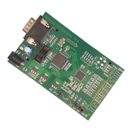
LVDS outputs of the TDC-GPX2. The SPI signals are available via additional pads [3]. A jumper selects the supply voltage as 3.0 V, 3.3 V or 3.6 V [4]. A separate jumper allows measuring the current into the TDC-GPX2 [5]. GPX2-EVA-Kit User Guide SC-001264-UG-5 / 2021-01-25 / Product... -
Page 6: Input Signals Lines
TDC-GPX2 via SPI [3] then remove 0Ohm resistors R75, R76 and R77 first [7]. Input Signals lines The board is prepared to connect directly CMOS input signals or LVDS signals. GPX2-EVA-Kit User Guide SC-001264-UG-5 / 2021-01-25 / Product... -
Page 7: Cmos Inputs
On the board there are 100kOhm pull-up resistors to TVDD33. The resistors interconnecting P and N inputs are not assembled. Software Description Main Window, REFCLK Page The software will start with the following main window: GPX2-EVA-Kit User Guide SC-001264-UG-5 / 2021-01-25 / Product... - Page 8 The first page, “REFCLK”, allows the user to select the reference input as well as the definition of the LSB. REFCLK_DIVISIONS defines the LSB at the output interface as fraction of the reference GPX2-EVA-Kit User Guide SC-001264-UG-5 / 2021-01-25 / Product...
-
Page 9: Stop Page
Various software filters, sinc or median, can be applied. STOP Page This page is for the PIN and HIT enable selection as well as the high resolution and combined channel settings. Figure 7: STOP page GPX2-EVA-Kit User Guide SC-001264-UG-5 / 2021-01-25 / Product... -
Page 10: Interface Page
Some combinations of parameter settings can prohibit operation or cause erroneous results. Some of these combinations are indicated with a red bar. User should avoid such configurations since the results may be difficult to interpret or faulty at all. Some examples of configuration conflicts: GPX2-EVA-Kit User Guide SC-001264-UG-5 / 2021-01-25 / Product... - Page 11 PUBLIC INFORMATION Figure 9: Avoiding conflicts Good Good Good Good The LVDS readout frequency is recommended up to 360MHz in SDR mode only. Nevertheless 400 MHz is possible to configure and operate GPX2-EVA-Kit User Guide SC-001264-UG-5 / 2021-01-25 / Product...
-
Page 12: Register Content
Changing the hexadecimal values will change the configuration in the GUI accordingly. With “Write Config” the updated configuration is downloaded into the chip. Figure 10: Registers Window: Configuration Figure 11: Registers Window: Results GPX2-EVA-Kit User Guide SC-001264-UG-5 / 2021-01-25 / Product... -
Page 13: Graph Window
The displayed data can be exported into a text file. The maximum is 128,000 data sets. Figure 13: Save data menu The text file can then be analyzed with a table calculation program. GPX2-EVA-Kit User Guide SC-001264-UG-5 / 2021-01-25 / Product... -
Page 14: Known Errors
This is most likely to erroneous reading from the FIFO and related in the FPGA. The error will be removed in the next revision of the FPGA. GPX2-EVA-Kit User Guide SC-001264-UG-5 / 2021-01-25 / Product... -
Page 15: Schematics, Layers And Bom
PUBLIC INFORMATION Schematics, Layers and BOM Figure 15: GPX2-EVA BOARD Schematics 1 GPX2-EVA-Kit User Guide SC-001264-UG-5 / 2021-01-25 / Product... - Page 16 PUBLIC INFORMATION Figure 16: GPX2-EVA BOARD Schematics 2 GPX2-EVA-Kit User Guide SC-001264-UG-5 / 2021-01-25 / Product...
- Page 17 PUBLIC INFORMATION Figure 17: GPX2-EVA BOARD Schematics 3 GPX2-EVA-Kit User Guide SC-001264-UG-5 / 2021-01-25 / Product...
- Page 18 PUBLIC INFORMATION Figure 18: GPX2-EVA BOARD Layout: Top layer Figure 19: GPX2-EVA BOARD Layout: GND Layer GPX2-EVA-Kit User Guide SC-001264-UG-5 / 2021-01-25 / Product...
- Page 19 PUBLIC INFORMATION Figure 20: GPX2-EVA BOARD Layout: VDD Layer Figure 21: GPX2-EVA BOARD Layout: Bottom layer GPX2-EVA-Kit User Guide SC-001264-UG-5 / 2021-01-25 / Product...
- Page 20 R25 R26 R27 R33 R35 R30 R31 165R CHIP-RESISTOR 0603 R75 R76 R77 CHIP-RESISTOR 0805 CHIP-RESISTOR 0805 R6 R67 R69 R71 R72 CHIP-RESISTOR 0805 CHIP-RESISTOR 0805 R17 R28 CHIP-RESISTOR 0805 R10 R51 100R CHIP-RESISTOR 0805 GPX2-EVA-Kit User Guide SC-001264-UG-5 / 2021-01-25 / Product...
- Page 21 Linear Voltage ADP163AUJZ-R7 Regulator U9 U12 Linear Voltage BD733L2FP3-CE2 Regulator 3,3V Male Connector 618015330923 DSUB15HD 90° Box Header Straight 1-1634688-0 10pin DC Power Jack PJ-059B J10 J11 J12 J13 Male Connector 2x1x180° 2,54 GPX2-EVA-Kit User Guide SC-001264-UG-5 / 2021-01-25 / Product...
-
Page 22: Copyrights & Disclaimer
ScioSense B.V. shall not be liable to recipient or any third party for any damages, including but not limited to personal injury, property damage, loss of profits, loss of use, interruption of business or indirect, special, incidental or consequential damages, of any kind, in connection with or arising out of the furnishing, performance or use of the technical data herein. -
Page 23: Document Status
Information in this datasheet is based on products which (Discontinued) conform to specifications in accordance with the terms of ScioSense B.V. standard warranty as given in the General Terms of Trade, but these products have been superseded and should not be used for new designs. - Page 24 ScioSense is a Joint Venture of ams AG Headquarters: ScioSense B.V. High Tech Campus 10 5656 AE Eindhoven The Netherlands Contact: www.sciosense.com info@sciosense.com...
Need help?
Do you have a question about the TDC-GPX2 and is the answer not in the manual?
Questions and answers