Table of Contents
Advertisement
QQ
3 7 63 1515 0
AUDIO/VIDEO MULTI-CHANNEL RECEIVER
VSX-LX53
VSX-2020-K
THIS MANUAL IS APPLICABLE TO THE FOLLOWING MODEL(S) AND TYPE(S).
Model
TE
L 13942296513
VSX-LX53
VSX-2020-K
This service manual should be used together with the following manual(s).
Model No.
VSX-LX53
VSX-2020-K
www
For details, refer to "Important Check Points for good servicing".
.
PIONEER CORPORATION
PIONEER ELECTRONICS (USA) INC. P.O. Box 1760, Long Beach, CA 90801-1760, U.S.A.
PIONEER EUROPE NV Haven 1087, Keetberglaan 1, 9120 Melsele, Belgium
PIONEER ELECTRONICS ASIACENTRE PTE. LTD. 253 Alexandra Road, #04-01, Singapore 159936
PIONEER CORPORATION
http://www.xiaoyu163.com
Type
SYXJ5
AC 220 V to 230 V
SYXJ5
AC 220 V to 230 V
Order No.
RRV4134
PCB RETRIEVAL DIAGRAM
x
ao
u163
y
i
1-1, Shin-ogura, Saiwai-ku, Kawasaki-shi, Kanagawa 212-0031, Japan
2010
http://www.xiaoyu163.com
2 9
8
STANDBY/ON
ADVANCED
iPod
B
A
N
D
T
U
N
E
MCACC
P
Q
L
S
H
D
M
I
iPhone
INPUT
AUTO SURR/ALC/
ADVANCED
STANDARD
MULTI-ZONE
SELECTOR
STREAM DIRECT
STEREO
SURROUND
SURROUND
HOME THX
SPEAKERS
CONTROL
ON/OFF
PHONES
iPod
iPhone
MCACC SETUP MIC
USB
VSX-LX53
Power Requirement
Q Q
3
6 7
1 3
1 5
Remarks
co
.
9 4
2 8
VSX-LX53
ENTER
P
R
E
S
E
T
T
U
N
E
R
E
D
T I
MASTER
VOLUME
VIDEO CAMERA
HDMI 5
Remarks
0 5
8
2 9
9 4
m
2010 Printed in Japan
K-FZV JUNE
9 9
ORDER NO.
RRV4133
2 8
9 9
Advertisement
Table of Contents

Related Manuals for Pioneer VSX-2020-K


Summarization of Contents
SERVICE PRECAUTIONS
NOTES ON SOLDERING
Notes on using lead-free solder and appropriate soldering irons for repairs.
NOTES ON REPLACING
Guidelines for replacing parts, especially discrete components, and replacing entire assemblies.
CAUTION
Cautions regarding discharging power and ground points for safe servicing.
SPECIFICATIONS
SPECIFICATIONS
Detailed technical specifications including audio, tuner, video, digital, control, and network sections.
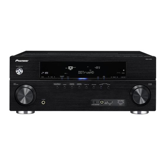
PANEL FACILITIES
Description of the front panel controls, indicators, and terminals.
Display Indicators
Signal and Format Indicators
Indicators related to signal input, format detection, tuner status, and decoding formats.
Listening Mode and Sound Indicators
Indicators for listening modes, multi-zone, sound controls, sleep mode, and speaker selection.
System Status and Control Indicators
Indicators for master volume, input function, scroll, and remote control modes.
Rear Panel Connectivity
HDMI and Video Inputs/Outputs
Description of HDMI, component video, and composite video connections.
Audio and Speaker Connections
Description of audio input/output jacks and speaker terminals.
Control and Network Interfaces
Description of control interfaces and network connectivity.
Power and Antenna Connections
Description of AC power input and antenna connections.
Remote Control Functions
RECEIVER Controls
Controls for receiver operation, including standby/on and zone control.
Input Function Selection
Buttons for selecting input functions and receiver control modes.
Receiver Setting and Operation
Buttons for TV control, audio/video parameters, and menu navigation.
Navigation and Volume Controls
Navigation buttons, master volume adjustment, and mute function.
Special Function Buttons
Buttons for multi-operation, TV control, multi-zone selection, and remote control LED.
BASIC ITEMS FOR SERVICE
CHECK POINTS AFTER SERVICING
Recommended check points to confirm product quality after servicing, covering video and audio.
PCB Locations and Identification
Main Processing and Digital Boards
Location of main processing, audio, component video, and DAC low assemblies.
Power and Interface Boards
Location of power, prestage, display, and regulator assemblies.
Ancillary and Connection Boards
Location of composite, front interface, binding, and bridge assemblies.
JIGS LIST
Jigs list
List of jigs required for diagnosis and service, including board-to-board extension jigs.
Lubricants and Glues List
List of lubricants and glues, such as Silicone Grease, specified for use.
BLOCK DIAGRAM
OVERALL WIRING DIAGRAM
Overall wiring diagram showing the interconnection of various assemblies and components.
Block Diagrams of Major Assemblies
Power Supply and Main Digital Boards
Block diagrams for power supply, encoder, digital main, and regulator assemblies.
Audio and Data Processing Boards
Block diagrams for audio, DAC, and bridge assemblies.
Front Panel and Binding Assemblies
Block diagrams for primary, front panel, and various binding assemblies.
Audio Block Components
HEADPHONE, POWER, and PRESTAGE Amplifiers
Block diagrams for headphone, power, and prestage amplifier sections.
Front Input and Audio Boards
Block diagrams for front input and audio processing boards.
Power Block Diagrams (Part 1)
Power Supply and Digital Main Boards
Block diagrams for power supply, DAC bridge, DAC low, component, and connect assemblies.
Power Amplification and Display Boards
Block diagrams for power amplifier and display assemblies.
Power Supply and Regulator Block Diagrams
Main Power Supply and Display
Block diagrams for display and XM regulator power supply.
Digital and Audio Processing Power
Block diagrams for power distribution to digital, audio, and bridge assemblies.
Amplification and Interface Power
Block diagrams for power supply to amplification, interface, and regulator sections.
DIAGNOSIS
DIAGNOSIS FLOWCHART
Flowchart for troubleshooting the 'No power problem' symptom, starting with the Ucom display.
Diagnosis Flowcharts
Main Ucom Power Supply Diagnosis
Flowchart for checking the power supply voltages for the main Ucom.
Main Ucom Crystal Diagnosis
Flowchart for checking the main Ucom crystal output and peripheral circuits.
Diagnosis Flowcharts (Continued)
MAIN Ucom Reset Procedures
Flowchart for resetting the main Ucom, checking connections and peripheral circuits.
Audio Section Troubleshooting
Distinguishing the Symptom
Distinguishing symptoms based on occurrence with specific functions or multiple functions.
Analog vs. Digital Problem Distinction
Differentiating problems between analog and digital signal paths.
Preout vs. Power Problem Distinction
Diagnosing issues related to pre-out output versus power amplifier problems.
AD Line vs. Digital Problem Distinction
Differentiating problems between AD (Analog-to-Digital) line and other digital signal paths.
DSP vs. Other Problem Distinction
Identifying issues within the DSP (Digital Signal Processor) section.
DIR vs. Other Problem Distinction
Troubleshooting problems related to the DIR (Digital Interface Receiver) circuit.
DSP&AUDIO Troubleshooting
DSP/AUDIO Troubleshooting Steps
Troubleshooting steps for DSP and audio signal issues.
DSP Power Supply Checks
Power supply checks for the DSP section.
DSP Crystal Oscillator Diagnosis
Diagnosis for the DSP crystal oscillator.
Troubleshooting Flowcharts (Continued)
DSP Reset Procedures
Procedures for resetting the DSP section.
Coaxial/Optical/AD Input Diagnosis
Troubleshooting for Coaxial, Optical, and AD input signals in stereo mode.
Troubleshooting Flowcharts (Continued)
Multi Channel Source Input Diagnosis
Flowchart for troubleshooting multi-channel source input, including DTS and Dolby.
XM Input Diagnosis
Diagnosis procedures for XM input signals.
Troubleshooting Flowcharts (Continued)
HDMI Signal Path Diagnosis
Diagnosis for HDMI signal output selection, covering SPDIF and I2S formats.
Troubleshooting Flowcharts (Continued)
Multi Channel Source Input Diagnosis
Troubleshooting for multi-channel source input signals.
XM Input Diagnosis
Troubleshooting for XM input signals.
Troubleshooting Flowcharts (Continued)
HDMI Signal Path Diagnosis
Diagnosis for HDMI signal output selection.
Troubleshooting Flowcharts (Continued)
USB/iPod Signal Path Diagnosis
Diagnosis for USB and iPod signal paths.
Internet Radio and XM Input Troubleshooting
Troubleshooting for Internet Radio and XM input, including zone control.
Bluetooth Adapter Port Diagnosis
Diagnosis for the Bluetooth adapter port connection.
Troubleshooting Flowcharts (Continued)
USB/iPod Signal Path Diagnosis
Diagnosis for USB and iPod signal paths.
HDMI Signal Path Diagnosis
Diagnosis for HDMI signal output selection.
Troubleshooting Flowcharts (Continued)
Zone Control, XM Radio, USB, and iPod Troubleshooting
Troubleshooting for Zone control, XM radio, USB, and iPod functions.
VIDEO Troubleshooting
Power Supply Checks for Video Output
Power supply checks for the video signal output.
Power Supply for XM Section
Power supply checks for the XM section.
Troubleshooting Flowcharts (Continued)
Video Block Crystal Diagnosis
Diagnosis for the video block crystal oscillator.
Video Block Reset Procedures
Reset procedures for the video block.
Troubleshooting Flowcharts (Continued)
General Video Troubleshooting
General troubleshooting for video signal output.
HDMI Input Diagnosis (IN BD, IN 1,5)
Diagnosis for HDMI input signals on specific ports.
Troubleshooting Flowcharts (Continued)
HDMI Input Diagnosis (IN 2,3,4)
Diagnosis for HDMI input signals on specific ports.
HDMI Output Troubleshooting
Troubleshooting procedures for HDMI output signals.
Troubleshooting Flowcharts (Continued)
Composite Input to HDMI Output Diagnosis
Diagnosis for composite input to HDMI output when DVC is ON.
Troubleshooting Flowcharts (Continued)
Component Input to HDMI Output Diagnosis (480p+)
Diagnosis for component input (480p+) to HDMI output with DVC ON.
Component Input to HDMI Output Diagnosis (480i)
Diagnosis for component input (480i) to HDMI output with DVC ON.
Troubleshooting Flowcharts (Continued)
Composite Input to Composite Output Diagnosis
Diagnosis for composite input to composite output when DVC is ON.
Component Input to Component Output Diagnosis (480i)
Diagnosis for component input (480i) to component output when DVC is ON.
Troubleshooting Flowcharts (Continued)
USB/iPod Signal Path Diagnosis
Diagnosis for USB and iPod signal paths.
Troubleshooting Flowcharts (Continued)
USB/iPod Signal Path Diagnosis
Diagnosis for USB and iPod signal paths.
Diagnosis and Circuit Descriptions
Protection Circuit Process List
List of protection circuit processes, including DC detection and AMP overload detection.
DC Detection Circuit Diagram
Schematic diagram of the DC detection circuit, showing transistors and ICs.
Circuit Descriptions (Continued)
OL (Over Load) Detection Circuit
Circuit diagram for detecting overloads in power supply sections.
Circuit Descriptions (Continued)
Protection Circuit Process List (XPROTECT)
Process list for XPROTECT detection, covering AMP power supply and transformer short circuits.
XPROTECT Circuit Diagram
Schematic diagram of the XPROTECT circuit, showing power supply and transformer protection.
Circuit Descriptions (Continued)
Protection Circuit Process List (XVDDERR)
Process list for XVDDERR detection, related to USB power failure.
XVDDERR Circuit Diagram
Schematic diagram of the XVDDERR circuit, detailing USB power failure detection.
Error Indications (Continued)
12V Trigger Error and Adapter Port Issues
Continuation of error indications, including 12V TRG ERR, NO ADAPTER, NOT AVAILABLE, and ADP OVERLOAD.
SERVICE MODE
TEST MODE
Information on entering and exiting TEST MODE, and basic operations for checking detection history.
Service Mode Operations
Error and Time Reset Functions
Procedures for resetting error counts and accumulated time data.
Test Mode States and Functions
Displaying and cycling through CEC and FAN test states.
USB Backup and Data Transfer
Operations for saving and loading USB backup data, including the CEC test function.
DISASSEMBLY
DISASSEMBLY
Preparations and procedures for disassembly, specifically for the POWER AMP ASSY, including discharging capacitors.
Diagnosis
Front Section Disassembly
Procedures for removing the front section of the unit, including exterior components and internal connections.
Front Section Disassembly Procedures
Release Cables and Binders
Steps for releasing cables and binders as needed during disassembly.
Unhook Hooks and Remove Front Section
Steps for unhooking the front section and removing it.
Front Section Disassembly and Diagnosis
Unhook HEADPHONE ASSY
Procedure for unhooking the headphone assembly.
Front Section Diagnosis
Diagnostic steps for the front section, involving connecting three connectors.
POWER AMP ASSY Removal and Diagnosis
Exterior Disassembly for Power Amp
Exterior disassembly steps for the power amplifier assembly, including screw removal and binder cutting.
Power Amp Diagnosis Procedures
Diagnostic steps for the power amplifier assembly, involving unit arrangement and rear panel grounding.
Power Amp Assy Disassembly and Diagnosis
Remove Locking Card Spacers
Procedure for removing locking card spacers.
Connect Rear Panel to Chassis Ground
Connecting the rear panel to the chassis ground as a diagnostic step.
Power Amp Assy Disassembly Procedures
Disconnect Connectors and Remove Power AMP Unit
Procedures for disconnecting connectors and removing the power amp unit.
Disconnecting Various Assemblies
Steps for disconnecting various assemblies from the main unit.
Power Amp Assy Disassembly Procedures (Continued)
Disconnect Connectors and Remove FFC
Disconnecting connectors, removing FFC, and cutting binders.
Remove Cushion Circles and Screws
Steps for removing cushion circles and screws.
Disconnect Connectors from CONNECT ASSY
Procedure for disconnecting connectors from the CONNECT ASSY.
Remove Rear Panel and Connectors
Steps for removing the rear panel and disconnecting connectors.
Power Amp Assy Disassembly and Assembly
Remove Locking Card Spacers and Rivets
Removing locking card spacers and nylon rivets.
Remove Screws and POWER AMP Assy
Removing screws and the power amp assembly.
Attach POWER AMP Assy to Heat Sink
Attaching the power amp assembly to the heat sink using screws and rivets.
Attach PRESTAGE Assy and Locking Card Spacers
Attaching the prestage assembly and locking card spacers.
Allocate and Fix POWER AMP Unit
Allocating the power amp unit, attaching screws, fixing to spacers, and connecting wires.
AUDIO ASSY Disassembly and Diagnosis
Exterior Disassembly for AUDIO ASSY
Exterior disassembly steps for the audio assembly, including bonnet removal, discharging capacitors, and releasing wires.
Audio Assembly Diagnosis
Diagnostic steps for the audio assembly, involving connecting three connectors and the rear panel to chassis ground.
Audio Assy Disassembly Procedures
Remove Screws and Nylon Rivet
Removing screws and nylon rivets from the assembly.
Disconnect Connectors and Remove Right Angle
Disconnecting connectors and removing the right angle component.
Audio Assy Disassembly and Diagnosis Procedures
Remove Rear Panel and Connectors
Removing the rear panel, AC inlet, and cushion circles.
Audio Assembly Diagnosis
Diagnostic steps for the audio assembly, involving arranging the unit and connecting the rear panel to chassis ground.
DAC LOW ASSY Disassembly and Diagnosis
Exterior Disassembly for DAC LOW ASSY
Exterior disassembly steps for the DAC LOW ASSY, including bonnet removal and discharging capacitors.
Remove Bridge Assemblies
Steps for removing D-DAC BRIDGE, A-DAC BRIDGE, and D-AUDIO BRIDGE assemblies.
Remove Six Screws
Procedure for removing six screws.
DAC LOW ASSY Disassembly and Diagnosis Procedures
Remove DAC LOW ASSY
Procedure for removing the DAC LOW ASSY.
D-AUDIO BRIDGE ASSY Reassembly and Diagnosis
Diagnostic steps for reassembling the D-AUDIO BRIDGE ASSY and connecting jig cables.
DAC LOW ASSY Diagnosis Procedures
Insert Insulation Sheet
Procedure for inserting the insulation sheet.
Connect DAC LOW Assy to Ground
Connecting the DAC LOW ASSY to the rear panel ground.
EACH SETTING AND ADJUSTMENT
SAVE AND LOAD SETTINGS USING USB MEMORY
Instructions for saving and loading unit settings using USB memory for backup and replacement.
HOW TO UPDATE FIRMWARE
Precautions for Firmware Update
Precautions regarding USB memory files, time/date, and HDMI control settings.
Firmware Update Procedure
Step-by-step procedure for updating firmware via USB memory, including panel mode and version confirmation.
Firmware Update Process
Entering Update Modes and File Searching
Instructions for entering update modes, checking versions, and searching for update files.
Update Confirmation and Completion
Steps for confirming the update status and completion.
Firmware Update Status and Confirmation
Update Completion Status
Status indicators for completed firmware updates on DSP, MAIN, and SUB components.
Update Confirmation and Time Required
How to confirm updated programs and information on the time required for updating.
EXPLODED VIEWS AND PARTS LIST
NOTES FOR PARTS LIST
Notes regarding part availability (NSP), safety factors (> mark), screw usage, and lubricant/glue application.
PACKING SECTION
Exploded view and parts list for the packing section of the unit.
PACKING SECTION PARTS LIST
PACKING SECTION PARTS LIST
List of parts included in the packing section of the VSX-LX53 and VSX-2020-K.
CONTRAST TABLE
Contrast table detailing differences in parts between VSX-LX53 and VSX-2020-K models.
EXTERIOR SECTION
EXTERIOR SECTION PARTS LIST
Detailed list of exterior parts with their mark numbers, descriptions, and part numbers.
Rear Panel Diagram
Rear Section Parts List
Detailed list of rear section parts with their mark numbers, descriptions, and part numbers.
Front Section Diagram
Front Section Parts List
Detailed list of front section parts with their mark numbers and part numbers.
SCHEMATIC DIAGRAM
AUDIO ASSY(1/3)(GUIDE PAGE)
Schematic diagram of the AUDIO ASSY, part 1 of 3, serving as a guide page.
AUDIO ASSY Schematics
AUDIO ASSY(1/3) (AWX9644)
Schematic diagram of the AUDIO ASSY (part 1/3), detailing component locations and connections.
Audio Assy Schematics (Continued)
AUDIO ASSY(1/3) (AWX9644)
Schematic diagram of the AUDIO ASSY (part 1/3), showing signal routes and component details.
Audio Assy Schematics (Continued)
AUDIO ASSY(1/3) (AWX9644)
Schematic diagram of the AUDIO ASSY (part 1/3), detailing resistors and capacitors.
Audio Assy Schematics (Continued)
AUDIO ASSY(1/3) (AWX9644)
Schematic diagram of the AUDIO ASSY (part 1/3), showing various ICs and connectors.
Audio Assy Schematics (Continued)
AUDIO ASSY(1/3) (AWX9644)
Schematic diagram of the AUDIO ASSY (part 1/3), detailing component locations and signal routes.
Audio Assy Schematics (Part 2)
AUDIO ASSY(2/3) (AWX9644)
Schematic diagram of the AUDIO ASSY (part 2/3), showing pre-buffer and PL2z selector circuits.
AUDIO ASSY(3/3)
AUDIO ASSY(3/3) (AWX9644)
Schematic diagram of the AUDIO ASSY (part 3/3), listing component values for PREBUFFER and TUNER sections.
Audio Assy Schematics (Part 3)
AUDIO ASSY(3/3) (AWX9644)
Schematic diagram of the AUDIO ASSY (part 3/3), listing component values for various sections like PHONO and tuner.
Composite Assy Schematic
COMPOSITE ASSY (AWX9568)
Schematic diagram of the COMPOSITE ASSY, detailing input and output signal paths.
DAC LOW ASSY(1/2)
DAC LOW ASSY(1/2) (AWX9657)
Schematic diagram of the DAC LOW ASSY, part 1 of 2, showing the DAC and ADC circuits.
DAC LOW ASSY Schematics (Part 1)
DAC LOW ASSY(1/2) (AWX9657)
Schematic diagram of the DAC LOW ASSY (part 1/2), illustrating digital interface and control logic.
DAC LOW ASSY(2/2)
DAC LOW ASSY(2/2) (AWX9657)
Schematic diagram of the DAC LOW ASSY, part 2 of 2, showing LPF and buffer circuits.
DAC LOW ASSY Schematics (Part 2)
DAC LOW ASSY(2/2) (AWX9657)
Schematic diagram of the DAC LOW ASSY (part 2/2), detailing power supply and filter circuits.
COMPONENT ASSY
COMPONENT ASSY (AWX9572)
Schematic diagram of the COMPONENT ASSY, showing signal routing and IC connections.
Component Assy Schematic
COMPONENT ASSY (AWX9572)
Schematic diagram of the COMPONENT ASSY, detailing video signal routes.
DIGITAL MAIN ASSY(1/10)(GUIDE PAGE)
DIGITAL MAIN ASSY(1/10) (AWX9719)
Schematic diagram of the DIGITAL MAIN ASSY, part 1 of 10, serving as a guide.
Digital Main Assy Schematics (Part 1)
DIGITAL MAIN ASSY(1/10) (AWX9719)
Schematic diagram of the DIGITAL MAIN ASSY (part 1/10), showing power supply and DDR connections.
Digital Main Assy Schematics (Part 1 Continued)
DIGITAL MAIN ASSY(1/10) (AWX9719)
Schematic diagram of the DIGITAL MAIN ASSY (part 1/10), showing flash ROM and DDR connections.
Digital Main Assy Schematics (Part 1 Continued)
DIGITAL MAIN ASSY (1/10) (AWX9719)
Schematic diagram of the DIGITAL MAIN ASSY (part 1/10), showing various ICs and their connections.
Digital Main Assy Schematics (Part 2)
DIGITAL MAIN ASSY(2/10) (AWX9719)
Schematic diagram of the DIGITAL MAIN ASSY (part 2/10), showing various ICs and their functions.
Digital Main Assy Schematics (Part 3)
DIGITAL MAIN ASSY(3/10) (AWX9719)
Schematic diagram of the DIGITAL MAIN ASSY (part 3/10), detailing power supplies and voltage regulators.
DIGITAL MAIN ASSY(4/10)
DIGITAL MAIN ASSY(4/10) (AWX9719)
Schematic diagram of the DIGITAL MAIN ASSY (part 4/10), showing various ICs and their connections.
Digital Main Assy Schematics (Part 4)
DIGITAL MAIN ASSY(4/10) (AWX9719)
Schematic diagram of the DIGITAL MAIN ASSY (part 4/10), detailing power supplies and voltage regulators.
DIGITAL MAIN ASSY(5/10)
DIGITAL MAIN ASSY(5/10) (AWX9719)
Schematic diagram of the DIGITAL MAIN ASSY (part 5/10), showing various ICs and signal routes.
DIGITAL MAIN ASSY(6/10)
DIGITAL MAIN ASSY(6/10) (AWX9719)
Schematic diagram of the DIGITAL MAIN ASSY (part 6/10), showing various ICs and their connections.
DIGITAL MAIN ASSY(7/10)
DIGITAL MAIN ASSY(7/10) (AWX9719)
Schematic diagram of the DIGITAL MAIN ASSY (part 7/10), showing power supplies and voltage regulators.
DIGITAL MAIN ASSY(8/10)
DIGITAL MAIN ASSY(8/10) (AWX9719)
Schematic diagram of the DIGITAL MAIN ASSY (part 8/10), showing various ICs and their connections.
DIGITAL MAIN ASSY(9/10)
DIGITAL MAIN ASSY(9/10) (AWX9719)
Schematic diagram of the DIGITAL MAIN ASSY (part 9/10), showing various ICs and their functions.
DIGITAL MAIN ASSY(10/10)
DIGITAL MAIN ASSY(10/10) (AWX9719)
Schematic diagram of the DIGITAL MAIN ASSY (part 10/10), showing various ICs and power supplies.
DIGITAL MAIN ASSY(11/10)
DIGITAL MAIN ASSY(11/10) (AWX9719)
Schematic diagram of the DIGITAL MAIN ASSY (part 11/10), showing various ICs and their connections.
DIGITAL MAIN ASSY(9/10)
DIGITAL MAIN ASSY(9/10) (AWX9719)
Schematic diagram of the DIGITAL MAIN ASSY (part 9/10), showing various ICs and their functions.
DIGITAL MAIN ASSY(10/10)
DIGITAL MAIN ASSY(10/10) (AWX9719)
Schematic diagram of the DIGITAL MAIN ASSY (part 10/10), showing various ICs and power supplies.
DIGITAL MAIN ASSY(9/10)
DIGITAL MAIN ASSY(9/10) (AWX9719)
Schematic diagram of the DIGITAL MAIN ASSY (part 9/10), showing various ICs and their functions.
DIGITAL MAIN ASSY(10/10)
DIGITAL MAIN ASSY(10/10) (AWX9719)
Schematic diagram of the DIGITAL MAIN ASSY (part 10/10), showing power supply and DDR connections.
DIGITAL MAIN ASSY(5/10)
DIGITAL MAIN ASSY(5/10) (AWX9719)
Schematic diagram of the DIGITAL MAIN ASSY (part 5/10), showing various ICs and their functions.
DIGITAL MAIN ASSY(6/10)
DIGITAL MAIN ASSY(6/10) (AWX9719)
Schematic diagram of the DIGITAL MAIN ASSY (part 6/10), showing various ICs and their connections.
DIGITAL MAIN ASSY(7/10)
DIGITAL MAIN ASSY(7/10) (AWX9719)
Schematic diagram of the DIGITAL MAIN ASSY (part 7/10), showing various ICs and power supplies.
DIGITAL MAIN ASSY(8/10)
DIGITAL MAIN ASSY(8/10) (AWX9719)
Schematic diagram of the DIGITAL MAIN ASSY (part 8/10), showing various ICs and their functions.
DIGITAL MAIN ASSY(9/10)
DIGITAL MAIN ASSY(9/10) (AWX9719)
Schematic diagram of the DIGITAL MAIN ASSY (part 9/10), showing various ICs and power supplies.
DIGITAL MAIN ASSY(10/10)
DIGITAL MAIN ASSY(10/10) (AWX9719)
Schematic diagram of the DIGITAL MAIN ASSY (part 10/10), showing various ICs and their functions.
POWER AMP ASSY(1/2)
POWER AMP ASSY(1/2) (AWX9660)
Schematic diagram of the POWER AMP ASSY (part 1/2), detailing transistor circuits and connections.
POWER AMP ASSY(2/2)
POWER AMP ASSY(2/2) (AWX9660)
Schematic diagram of the POWER AMP ASSY (part 2/2), showing regulator circuits and output stages.
POWER AMP ASSY(1/2)
POWER AMP ASSY(1/2) (AWX9660)
Schematic diagram of the POWER AMP ASSY (part 1/2), showing regulator circuits and protection.
POWER AMP ASSY(2/2)
POWER AMP ASSY(2/2) (AWX9660)
Schematic diagram of the POWER AMP ASSY (part 2/2), illustrating power supply and protection circuits.
PRESTAGE ASSY
PRESTAGE ASSY (AWX9580)
Schematic diagram of the PRESTAGE ASSY, showing amplifier circuits and connections.
PRESTAGE ASSY Schematics
PRESTAGE ASSY (AWX9580)
Schematic diagram of the PRESTAGE ASSY, detailing various amplifier stages.
DISPLAY ASSY
DISPLAY ASSY (AWX9669/AWX9726)
Schematic diagram of the DISPLAY ASSY, showing UCOM and other IC connections.
PRIMARY ASSY
PRIMARY ASSY (AWX9676)
Schematic diagram of the PRIMARY ASSY, showing power supply and transformer circuits.
PRIMARY ASSY Schematics
PRIMARY ASSY (AWX9676)
Schematic diagram of the PRIMARY ASSY, illustrating power supply regulators and protection.
USB REGULATOR ASSY
USB REGULATOR ASSY (AWX9581)
Schematic diagram of the USB regulator assembly, showing voltage regulation and protection.
XM REGULATOR ASSY
XM REGULATOR ASSY (AWX9667)
Schematic diagram of the XM regulator assembly, showing power supply and protection circuits.
REGULATOR ASSY
REGULATOR ASSY
Schematic diagram of the regulator assembly, showing various voltage regulators and protection circuits.
POWER SW, ENCODER and HEADPHONE ASSYS
POWER SW ASSY (AWX9588)
Schematic diagram of the power switch assembly.
ENCODER ASSY (AWX9589)
Schematic diagram of the encoder assembly.
HEADPHONE ASSY (AWX9590)
Schematic diagram of the headphone assembly.
CONNECT and A-DAC BRIDGE ASSYS
CONNECT ASSY (AWX9592)
Schematic diagram of the connect assembly.
A-DAC BRIDGE ASSY (AWX9571)
Schematic diagram of the A-DAC bridge assembly.
D-AUDIO BRIDGE ASSY
D-AUDIO BRIDGE ASSY (AWX9569)
Schematic diagram of the D-AUDIO bridge assembly.
D-DAC BRIDGE ASSY
D-DAC BRIDGE ASSY (AWX9570)
Schematic diagram of the D-DAC bridge assembly.
POS 1-3 ASSYS
POSI 1 ASSY (AWX9576)
Schematic diagram of the POSI 1 ASSY.
POSI 2 ASSY (AWX9577)
Schematic diagram of the POSI 2 ASSY.
POSI 3 ASSY (AWX9578)
Schematic diagram of the POSI 3 ASSY.
BIND L FRONT ASSY
BIND L FRONT ASSY (AWX9574)
Schematic diagram of the BIND L FRONT ASSY.
PCB CONNECTION DIAGRAM
AUDIO ASSY
PCB connection diagram for the AUDIO ASSY.
COMPOSITE ASSY
PCB connection diagram for the COMPOSITE ASSY.
DAC LOW ASSY
PCB connection diagram for the DAC LOW ASSY.
COMPONENT ASSY
PCB connection diagram for the COMPONENT ASSY.
DIGITAL MAIN ASSY
PCB connection diagram for the DIGITAL MAIN ASSY.
FRONT MIC&VIDEO and FRONT HDMI USB ASSYS
PCB connection diagrams for the FRONT MIC&VIDEO and FRONT HDMI USB ASSYS.
POWER AMP ASSY
PCB connection diagram for the POWER AMP ASSY.
PRESTAGE ASSY
PCB connection diagram for the PRESTAGE ASSY.
DISPLAY ASSY
PCB connection diagram for the DISPLAY ASSY.
PRIMARY ASSY
PCB connection diagram for the PRIMARY ASSY.
USB REGULATOR and XM REGULATOR ASSYS
PCB connection diagrams for USB and XM regulator assemblies.
REGULATOR ASSY
PCB connection diagram for the Regulator ASSY.
POWER SW, ENCODER and HEADPHONE ASSYS
PCB connection diagrams for power switch, encoder, and headphone assemblies.
CONNECT and A-DAC BRIDGE ASSYS
PCB connection diagrams for connect and A-DAC bridge assemblies.
D-AUDIO and D-DAC BRIDGE, POS 1-3 and BIND L FRONT ASSYS
PCB connection diagrams for D-AUDIO, D-DAC BRIDGE, POS 1-3, and BIND L FRONT assemblies.
BIND L BACK, BINDER, BIND DM CABLE, BIND R BACK/FRONT, BIND DISP FFC and BLUETOOH ASSYS
PCB connection diagrams for various binding and Bluetooth assemblies.
PCB PARTS LIST
AUDIO ASSY SEMICONDUCTORS
List of semiconductors used in the AUDIO ASSY.
DIGITAL MAIN ASSY SEMICONDUCTORS
List of semiconductors used in the DIGITAL MAIN ASSY.
MISCELLANEOUS
List of miscellaneous parts used in the DIGITAL MAIN ASSY.
RESISTORS
List of resistors used in the DIGITAL MAIN ASSY.
CAPACITORS
List of capacitors used in the DIGITAL MAIN ASSY.
Need help?
Do you have a question about the VSX-2020-K and is the answer not in the manual?
Questions and answers