Table of Contents
Advertisement
Specifications
Power Source
Power Consumption
Average use
Standby condition
Plasma Display panel
Drive method
Aspect Ratio
Contrast Ratio
Visible screen size
(No. of pixels)
Sound
Speaker
Audio Output
Headphones
PC signals
Receiving Systems /
Band name (PV60A)
Receiving Channels (PV60A)
AC 220-240 V, 50 / 60 Hz
341 W
0.3 W
AC type
16:9
Max 10000:1
106 cmV
920 mm (W) × 518 mm (H) × 1,056 mm (diagonal)
786,432 (1,024 (W) × 768 (H)) [3,072 × 768 dots]
12 cm × 6 cm × 2 pcs, 8 W
20 W (10 W + 10 W ), 10% THD
M3 (3.5 mm) Jack × 1
VGA, SVGA, XGA
SXGA
(compressed)
Horizontal scanning frequency 31 - 69 kHz
Vertical scanning frequency 59 - 86 Hz
VHF 0 to 12
UHF 21 to 69
S'1 to S'3
TH-42PV60A
TH-42PV60H
TH-42PV60M
TH-42PV60MT
GP9DE Chassis
PAL B
PAL G
HYPER TUNER
© 2006 Matsushita Electric Industrial Co., Ltd. All
rights
distribution is a violation of law.
ORDER NO.ITD0603006CE
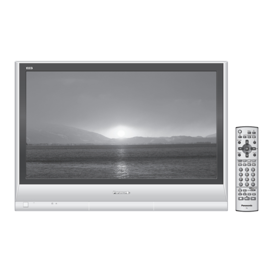
Plasma Television
reserved.
Unauthorized
copying
and
Advertisement
Table of Contents

Related Manuals for Panasonic TH-42PV60H


Summarization of Contents
Safety Precautions
General Guidelines
General guidelines for servicing, part replacement, and protective device installation.
Touch-Current Check
Procedure and limits for leakage current checks to prevent shock hazards.
Plasma Panel Replacement Method
Remove the Back cover
Instructions for removing the back cover of the TV chassis.
Remove the fan
Steps to disconnect couplers and remove the cooling fan.
Remove the tuner cover
Procedure for removing the tuner cover.
Remove the P-Board
Safety caution and steps to disconnect cables and remove the P-Board.
Remove the PA-Board
Steps to disconnect cables, flexible cables, and remove the PA-Board.
Remove the tuner unit
Instructions for removing the tuner unit after disconnecting cables and flexible cables.
Remove the DG-Board
Steps to disconnect couplers, flexible cables, and remove the DG-Board.
Remove the TA-Board
Procedure for disconnecting the tuner cable and removing the TA-Board.
Remove the H-Board
Steps to remove TA-Board, disconnect couplers, flexible cable, and remove H-Board.
Remove the HC-Board
Instructions to disconnect flexible cable and remove HC-Board.
Remove the D-Board
Steps to remove tuner unit, disconnect couplers, flexible cables, and remove D-Board.
Remove the SU-Board
Steps to remove screws, flexible cables, and slide SU-Board to disconnect.
Remove the SD-Board
Steps to remove screws, flexible cables, and slide SD-Board to disconnect.
Remove the SC-Board
Instructions to disconnect couplers, remove screws, and remove SC-Board.
Remove the SS-Board
Steps to disconnect couplers, flexible cables, remove screws, and remove SS-Board.
Remove the C1-Board
Steps to remove tuner unit, disconnect flexible cables and couplers, remove C1-Board.
Remove the C2-Board
Steps to remove tuner unit, disconnect flexible cables and couplers, remove C2-Board.
Remove the front bracket
Steps to unlock cable clampers, disconnect couplers, remove screws, and remove front bracket.
Remove the G-Board and GK-Board
Steps to remove front bracket, metal cover, front side metal frame, couplers, G-Board, and GK-Board.
Remove the speaker L, R
Steps to remove sponge, disconnect relay couplers, remove screws, and remove speakers.
Remove the S-Board
Steps to disconnect coupler, remove screws, and remove S-Board metal frame and S-Board.
Remove the K-Board
Steps to unlock cable clampers, disconnect coupler, remove screws, and remove K-Board.
Remove the stand brackets
Procedure to remove stand brackets after laying the panel face down.
Remove the Plasma panel section from the Front frame (glass)
Steps to remove front frame, stand brackets, and pull out the plasma panel.
Replace the plasma panel (finished)
Steps to attach boards, hooks, stand brackets, and front frame for the new plasma panel.
Location of Lead Wiring
Lead of Wiring (1)
Diagram showing the dressing of wires and a table for connector numbers.
Lead of Wiring (2)
Diagram showing wire dressing and a table for connector numbers.
Lead of Wiring (3)
Diagram showing wire dressing and a table for connector numbers.
Lead of Wiring (4)
Diagram showing wire dressing and a table for connector numbers.
Lead of Wiring (5)
Diagram showing wire dressing for fans and a table for connector numbers.
Lead of Wiring (6)
Diagram showing wire dressing and a table for connector numbers.
Self Check and Troubleshooting
Self Check Procedure
How to enter self-check mode and check bus lines/hexadecimal codes.
Power LED Blinking Chart
Information on LED flashing timings to identify defective blocks during abnormalities.
No Power Troubleshooting
Troubleshooting guide for no power indication states based on power LED.
No Picture Troubleshooting
Troubleshooting flowchart for issues related to no picture display.
Local Screen Failure
Explanation of local area failures on the plasma display and possible defective PCBs.
Service Mode Functions
How to Enter SERVICE 1 Mode
Steps to enter SERVICE 1 mode using the remote control and TV set buttons.
How to Enter SERVICE 2 Mode
Steps to enter SERVICE 2 mode using channel, EQ, and remote control buttons.
Option Description
Detailed description of various option codes and their functions for different models.
Adjustment Procedures
Driver Set-up
Preparation and adjustments for driver section voltages using panel data.
Initialization Pulse Adjust
Procedure for adjusting initialization pulse using an oscilloscope.
P.C.B. Exchange and Adjustment
Cautionary notes and quick adjustment steps after exchanging a PCB.
Adjustment Volume Location
Diagrams showing the location of adjustment volumes on the boards.
Test Point Location
Diagrams indicating the location of test points for adjustments.
Picture Adjustments
PAL Panel White Balance Adjustment
Procedure for adjusting white balance using a color analyzer and service mode.
HD White Balance Adjustment
Procedure for adjusting white balance for HD signals using a color analyzer.
Sub Bright Adjustment
Procedure for adjusting sub-bright using a gray-scale pattern and service mode.
ABL Adjustment
Procedure for adjusting Automatic Brightness Limiter (ABL) based on power consumption.
Sub-Contrast Adjustment
Procedure for adjusting sub-contrast for AV, RF, and HD systems.
Multi-Window Adjustment
Procedure for adjusting video gain for multi-window display to make screen borderline unremarkable.
Board Conductor Views
P-Board Conductor View
Illustration of the P-Board foil side with grid references.
PA-Board Conductor View
Illustration of the PA-Board foil and component sides with grid references and parts location.
H, HC, and TA-Board Conductor Views
Illustrations of H, HC, and TA boards (foil side) with grid references and parts location.
G-Board Conductor Views
Illustrations of G-Board (foil and component sides) with grid references.
GK, K, and S-Board Conductor Views
Illustrations of GK, K, and S boards (foil and component sides) with grid references.
DG-Board Conductor View
Illustration of DG-Board (foil side) with grid references and parts location.
D-Board Conductor View
Illustration of D-Board (foil side) with grid references and parts location.
C1-Board Conductor Views
Illustrations of C1-Board (foil and component sides) with grid references and parts location.
C2-Board Conductor Views
Illustrations of C2-Board (foil and component sides) with grid references and parts location.
SC-Board Conductor View
Illustration of SC-Board (foil side) with grid references and parts location.
SU-Board Conductor Views
Illustrations of SU-Board (foil and component sides) with grid references and parts location.
SD-Board Conductor Views
Illustrations of SD-Board (foil and component sides) with grid references and parts location.
SS-Board Conductor View
Illustrations of SS-Board (foil side) with grid references and parts location.
Schematic and Block Diagrams
Schematic Diagram Notes
Important notes and symbols used in schematic diagrams.
Main Block Diagram
Block diagram illustrating the main functional components and their interconnections.
P-Board Block Diagram
Block diagram detailing the P-Board's functional components and power supply circuits.
P-Board (1 of 6) Schematic Diagram
Schematic diagram of the P-Board, part 1 of 6.
P-Board (2 of 6) Schematic Diagram
Schematic diagram of the P-Board, part 2 of 6.
P-Board (3 of 6) Schematic Diagram
Schematic diagram of the P-Board, part 3 of 6.
P-Board (4 of 6) Schematic Diagram
Schematic diagram of the P-Board, part 4 of 6.
P-Board (5 of 6) Schematic Diagram
Schematic diagram of the P-Board, part 5 of 6.
P-Board (6 of 6) Schematic Diagram
Schematic diagram of the P-Board, part 6 of 6.
PA-Board Block Diagram
Block diagram illustrating the PA-Board's components and functions.
PA-Board (1 of 3) Schematic Diagram
Schematic diagram of the PA-Board, part 1 of 3.
PA-Board (2 of 3) Schematic Diagram
Schematic diagram of the PA-Board, part 2 of 3.
PA-Board (3 of 3) Schematic Diagram
Schematic diagram of the PA-Board, part 3 of 3.
H and TA-Board Block Diagram
Block diagram illustrating the H and TA boards and their connections.
G, GK, and K-Board Schematic Diagram
Schematic diagrams for G, GK, and K boards.
HC and TA-Board Schematic Diagram
Schematic diagrams for HC and TA boards.
DG-Board (1 of 3) Block Diagram
Block diagram of the DG-Board, part 1 of 3, showing HDMI interface and MICOM.
DG-Board (2 of 8) Schematic Diagram
Schematic diagram of the DG-Board, part 2 of 8.
DG-Board (3 of 8) Schematic Diagram
Schematic diagram of the DG-Board, part 3 of 8.
DG-Board (4 of 8) Schematic Diagram
Schematic diagram of the DG-Board, part 4 of 8.
DG-Board (5 of 8) Schematic Diagram
Schematic diagram of the DG-Board, part 5 of 8.
DG-Board (6 of 8) Schematic Diagram
Schematic diagram of the DG-Board, part 6 of 8.
DG-Board (7 of 8) Schematic Diagram
Schematic diagram of the DG-Board, part 7 of 8.
DG-Board (8 of 8) Schematic Diagram
Schematic diagram of the DG-Board, part 8 of 8.
D-Board Block Diagram
Block diagram of the D-Board, illustrating its components and functions.
D-Board (1 of 6) Schematic Diagram
Schematic diagram of the D-Board, part 1 of 6.
D-Board (2 of 6) Schematic Diagram
Schematic diagram of the D-Board, part 2 of 6.
D-Board (3 of 6) Schematic Diagram
Schematic diagram of the D-Board, part 3 of 6.
D-Board (4 of 6) Schematic Diagram
Schematic diagram of the D-Board, part 4 of 6.
D-Board (5 of 6) Schematic Diagram
Schematic diagram of the D-Board, part 5 of 6.
D-Board (6 of 6) Schematic Diagram
Schematic diagram of the D-Board, part 6 of 6.
C1 and C2-Board Block Diagrams
Block diagrams illustrating the C1 and C2 boards and their data drive functions.
C1-Board (1 of 2) Schematic Diagram
Schematic diagram of the C1-Board, part 1 of 2.
C1-Board (2 of 2) Schematic Diagram
Schematic diagram of the C1-Board, part 2 of 2.
C2-Board (1 of 2) Schematic Diagram
Schematic diagram of the C2-Board, part 1 of 2.
C2-Board (2 of 2) Schematic Diagram
Schematic diagram of the C2-Board, part 2 of 2.
SC, SU, and SD-Board Block Diagrams
Block diagrams illustrating SC, SU, and SD boards, including scan drive and data driver functions.
SC-Board (1 of 2) Schematic Diagram
Schematic diagram of the SC-Board, part 1 of 2.
SC-Board (2 of 2) Schematic Diagram
Schematic diagram of the SC-Board, part 2 of 2.
SU-Board (1 of 2) Schematic Diagram
Schematic diagram of the SU-Board, part 1 of 2.
SU-Board (2 of 2) Schematic Diagram
Schematic diagram of the SU-Board, part 2 of 2.
SD-Board (1 of 2) Schematic Diagram
Schematic diagram of the SD-Board, part 1 of 2.
SD-Board (2 of 2) Schematic Diagram
Schematic diagram of the SD-Board, part 2 of 2.
SS and S-Board Block Diagram
Block diagrams illustrating SS and S boards, including power switch and sustain drive functions.
SS and S-Board Schematic Diagram
Schematic diagrams for SS and S-Board.
Parts Location and Mechanical Replacement Parts List
Parts Location
Diagrams showing the location of various mechanical parts on the TV chassis.
Packing Exploded Views (1)
Exploded view diagrams illustrating packing components.
Packing Exploded Views (2)
Exploded view diagrams illustrating packing components.
Packing Exploded Views (3)
Exploded view diagrams illustrating packing components.
Mechanical Replacement Parts List
List of mechanical parts with part numbers, descriptions, quantities, and remarks.
Electrical Replacement Parts List
Replacement Parts List Notes
Notes regarding replacement parts, including retention time and abbreviations.
Electrical Replacement Parts List
List of electrical replacement parts with part numbers, descriptions, and quantities.
Need help?
Do you have a question about the TH-42PV60H and is the answer not in the manual?
Questions and answers