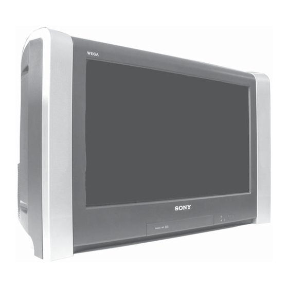
Summarization of Contents
AE-6BA Self Diagnostic Software
Table 1: Error Messages and LED Codes
Lists error messages with corresponding LED blink codes for troubleshooting.
Table 2: Error Monitor and Counters
Displays error counts stored in NVM and working time.
A Board Technical Data
A Board Semiconductor Voltage Table
Lists voltage readings for semiconductors on the A board.
A Board Waveforms
Displays typical waveform patterns for testing on the A board.
A Board IC Voltage Table
Provides voltage measurements for IC pins on the A board.
A Board Location Tables
Shows component locations on A board sides A and B.
A Board Difference Table
Lists differences between models KV-32XL90B and KV-32XL90E.
A Board Schematics
A Board Schematic Diagram [Audio, Deflection J Interface]
Circuit diagram for audio and deflection interfaces on the A board.
A Board Schematic Diagram [Tuner, Regulators]
Circuit diagram for tuner and regulator sections on the A board.
A Board Schematic Diagram [B Interface]
Circuit diagram for the B interface on the A board.
B Board Schematics
B Board Schematic Diagram [Backend, Scanrate, LVDS,A_Interface] Page 1/3
Circuit diagram for backend, scanrate, LVDS, and A interface on the B board.
B Board Schematic Diagram [Backend, Scanrate, LVDS,A_Interface] Page 2/3
Circuit diagram for backend, scanrate, LVDS, and A interface on the B board.
B Board Schematic Diagram [Backend, Scanrate, LVDS,A_Interface] Page 3/3
Circuit diagram for backend, scanrate, LVDS, and A interface on the B board.
Various Board Schematics and Data
F1 Board Schematic Diagram [Power Switch, Fuse, SIRCS and Stand-By LED]
Circuit diagram for power switch, fuse, and stand-by LED.
VM Board Schematic Diagram [Velocity Modulation]
Circuit diagram for velocity modulation.
H5 Board Schematic Diagram [Front AV Input, Headphone and Control Switches]
Circuit diagram for AV input, headphone, and control switches.
VM Board Voltage Table and Waveforms
Voltage and waveform data for the VM board.
G Board Schematic Diagram
G Board Schematic Diagram [Power Supply]
Circuit diagram for the power supply section of the G board.
C Board Schematic Diagram
C Board Schematic Diagram [R-G-B Out]
Circuit diagram for R-G-B output signals on the C board.
J Board Schematic Diagram
J Board Schematic Diagram [AV Scart I/O Switching and Sockets ]
Circuit diagram for AV scart I/O and sockets on the J board.
MS Board Schematics
MS Board Schematic Diagram [Trimedia Memory Stick ] Page 1/3
Circuit diagram for the Trimedia Memory Stick interface (Part 1).
MS Board Schematic Diagram [Trimedia Memory Stick ] Page 2/3
Circuit diagram for the Trimedia Memory Stick interface (Part 2).
MS Board Schematic Diagram [Trimedia Memory Stick ] Page 3/3
Circuit diagram for the Trimedia Memory Stick interface (Part 3).
D2 Board Schematic Diagram
D2 Board Schematic Diagram [Smart Mode Deflection ]
Circuit diagram for smart mode deflection on the D2 board.
D Board Schematic Diagram
D Board Schematic Diagram [Deflection ]
Circuit diagram for deflection signals on the D board.


Need help?
Do you have a question about the Trinitron KV-32XL90E and is the answer not in the manual?
Questions and answers