Advertisement
Quick Links
Advertisement

Summary of Contents for Elba ZX-128A1
- Page 1 ZX-128A1 Development Board Reference Manual Version 1.0...
- Page 2 – First public release Disclaimer Elba Corp. makes no warranty regarding the accuracy of or the fitness for any particular purpose of the information in this document or the techniques described herein. The reader assumes the entire responsibility for the evaluation of and use of the information presented.
- Page 3 Table of Contents Introduction........................... 1 Preparation for Use........................1 Connections and Jumpers ......................1 J1-J10............................1 J13, J12............................ 1 J13 ............................1 J14 ............................2 J15 ............................2 J16 ............................2 J17 ............................2 J18 ............................2 J19 ............................2 J20 ............................
- Page 4 This page is intentionally blank.
-
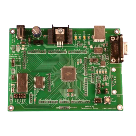
Page 5: Preparation For Use
The jumpers and switches are set at the factory assuming that the Dev Board will be powered via the on-board regulator and that a standard serial port will be used for communication with the ZX-128A1. If this is how you intend to operate it, simply connect an external supply to J23, connect your serial cable to J24 and activate the power switch. - Page 6 This Atmel-standard 6-pin header is used for programming the mega128A1 chip. In normal use, these signals are not useful to end-users but they may be useful if the Dev Board is being used in an unconventional way. This two-pin connection provides access to the transmit and receive signals of the USB port. This is most useful if the USB port is not being used as the primary serial interface for Com1.
- Page 7 J25 like Digi-Key # A32117-ND or Mouser # 571-5747844-4. Unless the configuration jumpers/switches are set to use the USB port, J24 is connected to Com1 of the ZX-128A1. If J25 is installed, J38 is used to access the logic-level transmit and receive signals. SIP sockets installed in J38 may simplify such connections.
- Page 8 The schematics on the following pages document the circuitry on the Dev Board. They may be useful for gaining a better understanding of the effects of the various switch and jumper positions. They may also be useful for deriving ideas for your own ZX-128A1 project.
Need help?
Do you have a question about the ZX-128A1 and is the answer not in the manual?
Questions and answers