Table of Contents
Advertisement
Quick Links
Astronics T940-001
64-Channel Digital Resource Module
A l l t r a d e m a r k s , b r a n d n a m e s , a n d b r a n d s a p p e a r i n g h e r e i n a r e t h e p r o p e r t y o f t h e i r r e s p e c t i v e o w n e r s .
• C r i t i c a l a n d e x p e d i t e d s e r v i c e s
• I n s t o c k / R e a d y - t o - s h i p
Artisan Scientific Corporation dba Artisan Technology Group is not an affiliate, representative, or authorized distributor for any manufacturer listed herein.
In Stock
Used and in Excellent Condition
Open Web Page
https://www.artisantg.com/75340-16
• We b u y y o u r e x c e s s , u n d e r u t i l i z e d , a n d i d l e e q u i p me n t
• F u l l - s e r v i c e , i n d e p e n d e n t r e p a i r c e n t e r
Advertisement
Table of Contents

Related Manuals for Astronics Talon Instruments T940

Summary of Contents for Astronics Talon Instruments T940
- Page 1 Astronics T940-001 64-Channel Digital Resource Module In Stock Used and in Excellent Condition Open Web Page https://www.artisantg.com/75340-16 A l l t r a d e m a r k s , b r a n d n a m e s , a n d b r a n d s a p p e a r i n g h e r e i n a r e t h e p r o p e r t y o f t h e i r r e s p e c t i v e o w n e r s .
- Page 2 Tel: (800) 722-2528, (949) 859-8999; Fax: (949) 859-7139 atsinfo@astronics.com atssales@astronics.com atshelpdesk@astronics.com http://www.astronicstestsystems.com Copyright 2009 by Astronics Test Systems Inc. Printed in the United States of America. All rights reserved. This book or parts thereof may not be reproduced in any form without written permission of the publisher.
-
Page 3: Warranty Statement
This warranty does not apply to defects resulting from any modification(s) of any product or part without Astronics Test Systems express written consent, or misuse of any product or part. The warranty also does not apply to fuses, software, non-rechargeable batteries, damage from battery leakage, or problems arising from normal wear, such as mechanical relay life, or failure to follow instructions. -
Page 4: Return Of Product
This document and the technical data herein disclosed, are proprietary to Astronics Test Systems, and shall not, without express written permission of Astronics Test Systems, be used in whole or in part to solicit quotations from a competitive source or used for manufacture by anyone other than Astronics Test Systems. -
Page 5: For Your Safety
FOR YOUR SAFETY Before undertaking any troubleshooting, maintenance or exploratory procedure, read carefully the WARNINGS and CAUTION notices. This equipment contains voltage hazardous to human life and safety, and is capable of inflicting personal injury. If this instrument is to be powered from the AC line (mains) through an autotransformer, ensure the common connector is connected to the neutral (earth pole) of the power supply. -
Page 6: Table Of Contents
Chapter 3 ........................3-1 DRM Front Panel ......................3-1 J200 and J201 DRA Channel I/O ....................3-2 PWR Connector – DRA/DRB Power and Signals ................3-2 Front Panel Connectors ........................3-3 Front Panel LBUS Lockout Keys ....................3-4 Astronics Test Systems... - Page 7 Chapter 5 ......................... 5-1 Soft Front Panel Operation ..................... 5-1 SFP Basics ............................. 5-1 SFP Main Panel ......................... 5-2 Company Logo ........................5-4 Active LED ..........................5-4 Chassis Data .......................... 5-4 Module Data ........................... 5-4 Title Bar ..........................5-4 Astronics Test Systems...
- Page 8 MPSIG Signal ........................5-22 Error Pulse Width ........................5-23 Record Mode ........................5-23 Config Data Sequencer A/B ..................... 5-24 Configure Clocks ........................5-24 Master Clock ........................5-25 System Clock ........................5-26 External Mode ........................5-26 External Offset ........................5-27 Astronics Test Systems...
- Page 9 Over-Current ........................5-43 Channel and Global Disable..................5-43 Over-Current Window ....................5-43 Drive Fault ........................5-44 Probe ..........................5-45 Probe State ........................5-45 Offset ..........................5-46 Probe Data ........................5-46 CRC Capture ......................... 5-46 Probe Button ......................... 5-47 Astronics Test Systems...
- Page 10 Configure UR14 Channel Properties ..................5-64 Compare Input (V) ........................ 5-65 OC Detect (A) ........................5-65 All Channels .......................... 5-65 Configuring the AUX Channels ..................... 5-65 Configuring the AUX/UAUX Signals ..................5-68 State ............................. 5-69 Source ..........................5-69 Astronics Test Systems...
- Page 11 Set Vector Bits........................5-95 Source ..........................5-95 Input Mode ........................5-96 Set Vector Table ........................5-96 Vector Bit Index ........................ 5-97 Vector Jump Step ......................5-97 Timing Set ........................5-97 Set Channel Test ......................... 5-97 Expect ..........................5-98 Astronics Test Systems...
- Page 12 Burst Error LED ........................5-116 Errors ..........................5-116 Power Converter Alert ......................5-116 D/R Alert ..........................5-116 Sequence Active ......................... 5-117 Step Number ........................5-117 Pattern Address ........................5-117 Record Count ........................5-117 Timing Set ........................... 5-117 Astronics Test Systems...
- Page 13 CRC Save File Format ....................5-129 Error Address Save File Format ..................5-130 Record Index Save File Format ..................5-130 Record Data Save File Format ..................5-130 Probe Data Save File Format ..................5-131 CRCs Display ........................5-131 viii Astronics Test Systems...
- Page 14 PMU Panel ..........................5-155 Channel ..........................5-156 Measure Voltage ......................... 5-156 Instrument Functions ........................5-156 Self Test..........................5-156 Full RAM Test ......................... 5-158 Power Converter Test ......................5-158 Calibration Panel ........................5-159 Driver/Receiver ........................5-160 Calibrate Function ....................... 5-160 Astronics Test Systems...
- Page 15 SFP Close Message ......................5-176 Chapter 6 ......................... 6-1 Programmable Channel Calibration ................6-1 Performance Verification ........................ 6-1 Environmental Conditions ......................6-2 Voltage Mode ..........................6-2 V+ and V- Requirements ........................ 6-2 Warm-up Period ..........................6-2 Recommended Test Equipment ..................... 6-2 Astronics Test Systems...
- Page 16 IAL/IAH ............................. 6-23 Select Calibrate Function ..................... 6-23 Select Start and End Channels and Measurement Delay ............ 6-23 DRM Calibration Warmup ..................... 6-24 Run Calibration ........................6-24 Chapter 7 ........................7-1 Specifications ......................... 7-1 Timing Characteristics ........................7-1 Astronics Test Systems...
- Page 17 Pattern Control Instructions ..................... 8-35 Pattern Control Instruction Details ................... 8-37 T964 VXI Backplane Trigger Bus ....................8-42 Trigger Bus description: ......................8-42 Trigger Bus Applications: ......................8-42 Normal Operation: ........................8-43 Normal Operation Example: ..................... 8-43 Astronics Test Systems...
- Page 18 Control Logic ..........................C-4 Signal Descriptions ........................ C-5 Firmware & NV Data ........................C-5 Signal Descriptions ........................ C-5 DR2 Characteristics ........................C-5 Power Requirements ........................C-6 Environmental ..........................C-6 DR2 Signal Description........................C-7 DRA I/O Channels (J200) ......................C-7 Astronics Test Systems xiii...
- Page 19 Signal Descriptions ........................ E-6 Power Configuration........................E-6 DR4 Characteristics ........................E-7 Power Requirements ........................E-8 Environmental ..........................E-8 DR4 Signal Description ........................E-9 DRA I/O Channels (J200) ......................E-9 DRB I/O Channels (J201) ......................E-11 Calibration ............................ E-12 Astronics Test Systems...
- Page 20 Signal Descriptions ........................ G-5 DR8 Characteristics ........................G-5 Power Requirements ........................G-6 Environmental ..........................G-6 DR8 Signal Description........................G-7 DRA I/O Channels (J200) ......................G-7 DRB I/O Channels (J201) ......................G-9 PWR Connector ........................G-11 Calibration ............................ G-12 Astronics Test Systems...
- Page 21 ADC Voltage and Temperature Monitoring ................I-13 Signal Descriptions (Figure I-9) ..................... I-13 UR14 Control Logic ........................I-15 Firmware and Calibration Storage .................... I-15 External Probe Module Block Diagram ..................I-15 Signal Descriptions (Figure I-10)................... I-16 External Probe Module ........................I-18 Astronics Test Systems...
- Page 22 External Start Setup Time to T0CLK In ..................J-4 External Stop Setup Time to T0CLK In ..................J-4 A Channel Input to TRG Bus (for a channel test) ............... J-4 SEQ_ACT/IDLE_ACT/Sync Pulse/Seq. Flag to TRG Bus ............J-4 Astronics Test Systems xvii...
- Page 23 Model T940 User Manual Publication No. 980938 Rev. K This page was left intentionally blank. xviii Astronics Test Systems...
- Page 24 Figure 5-16: Configure Linked Trigger Bus Panel ................5-14 Figure 5-17: Configure Group Panel ....................5-15 Figure 5-18: Set VXI Triggers DSA Panel ..................5-19 Figure 5-19: Configure DSn D/R Properties Panel ................5-21 Figure 5-20: Configure Data Sequencer ..................5-24 Astronics Test Systems...
- Page 25 Figure 5-60: Edit Pattern Set Panel ....................5-108 Figure 5-61: Sequence Step Properties Panel ................5-109 Figure 5-62: Executing a Sequence Panel ................... 5-112 Figure 5-63: Execute State Diagram ..................... 5-113 Figure 5-64: Set Sync Panel ......................5-122 Astronics Test Systems...
- Page 26 Figure 5-103: DR4 Voltage Monitoring Panel ................5-171 Figure 5-104: DR3e Chip Temperature ..................5-173 Figure 5-105: DR9 Chip Temperature ................... 5-174 Figure 5-106: UR14 Chip Temperature ..................5-174 Figure 5-107: Utility Reference Monitor ..................5-175 Figure 5-108: SFP Close Message ....................5-176 Astronics Test Systems...
- Page 27 Figure D-6: Front Panel Optional DR3e PWR Connector .............. D-17 Figure E-1: DR4 I/O Block Diagram ....................E-2 Figure E-2: DR4 Driver/Receiver Block Diagram ................E-4 Figure E-3: Auxiliary Driver & Receiver I/O Block Diagram .............. E-5 Figure E-4: DR4 Power Configuration ....................E-6 xxii Astronics Test Systems...
- Page 28 Figure I-11: External Probe Module Flush Mount ................I-18 Figure I-12: External Probe Module Right Angle ................I-18 Figure I-13: External Probe Module with Probe ................I-19 Figure I-14: Front Panel Connectors ....................I-28 Figure I-15: UR14 J9 Calibration and Signal Connectors ..............I-33 Astronics Test Systems xxiii...
- Page 29 Model T940 User Manual Publication No. 980938 Rev. K This page was left intentionally blank. xxiv Astronics Test Systems...
- Page 30 Table 5-24: Synthesizer Ref Source Settings ................. 5-27 Table 5-25: Watchdog Action ......................5-29 Table 5-26: Watchdog Timer Resolution Ranges ................5-30 Table 5-27: Sequence Timeout State Action ................... 5-30 Table 5-28: Trigger Settings ......................5-32 Table 5-29: Trigger Source Settings....................5-33 Astronics Test Systems...
- Page 31 Table 5-68: Input Bus Select Source Settings ................5-70 Table 5-69: ECL Mode Settings ...................... 5-71 Table 5-70: Logic Mode Settings ....................5-72 Table 5-71: Probe Expect Codes ....................5-84 Table 5-72: Pattern Codes ......................5-86 Table 5-73: ASCII/Binary Data Format ................... 5-88 xxvi Astronics Test Systems...
- Page 32 Table 8-1: Summary of When Specific DRS Signals are Needed ............ 8-5 Table 8-2: Summary of the Record Memory Action for each Step Record Mode ......8-7 Table 8-3: Summary of the Record Memory Action for each Step Record Mode ......8-9 Astronics Test Systems xxvii...
- Page 33 Table F-2: DR7 Power Requirements ....................F-6 Table F-3: DR7, DRA I/O Channels (J200) ..................F-7 Table F-4: DR7 Pinout by Pin Number (DRA) .................. F-8 Table F-5: DR7, DRB I/O Channels (J201) ..................F-10 Table F-6: Calibration Settings......................F-10 xxviii Astronics Test Systems...
- Page 34 Table I-15: J2A Connector Pinout by Pin Number ................I-31 Table I-16: J3B Connector Pinout by Pin Number ................I-32 Table I-17: J1A Connector Pinout by Pin Number ................I-32 Table I-18: J1B Connector Pinout by Pin Number ................I-32 Astronics Test Systems xxix...
-
Page 35: Document Change History
ECN04897: Added additional content including attributes and static state control, statis mode, comparator delay, pass/fail clear, and static data. 5/7/2014 Revised MTBF hours for boards. Rebranded manual to Astronics. ECN05018: Added information regarding new DR4 6/13/2014 option including Appendix E, DR4 Driver/Receiver Board. -
Page 36: Chapter 1
DRM front panel power and additional cooling for large digital test systems. (See an illustration of the chassis in Chapter 2, Installation). For additional information on this chassis, contact your sales representative. Astronics Test Systems Introduction 1-1... -
Page 37: Application Layer
The optional Microsoft Windows® CIIL Emulation Module (WCEM), for the Astronics Test Systems PAWS™ Runtime System (RTS), provides an interface to the DRM from the IEEE standard ATLAS test language for modern test development. - Page 38 Channels may be set up either individually or in user-defined groups. WCEM for Astronics Test Systems PAWS The optional WCEM for the PAWS Runtime system provides an interface to the DRM from the IEEE standard ATLAS test language. This interface provides the...
-
Page 39: Driver/Receiver Board Options
Programmable current load with dual commutating voltages • Selectable resistive input load (8 choices) to a programmed voltage • Selectable output slew rate (0.25 V/ns to 1.3 V/ns) • 12/50 Ohm selectable output impedance • Over-current detection Introduction 1-4 Astronics Test Systems... - Page 40 Four TTL with selectable output impedance and resistive input load. Four TTL Four ECL (single ended or differential) DR9: Driver/Receiver The DR9 features: • Channels: 24 single-ended variable voltage or 12 differential channels and 24 analog test channels Astronics Test Systems Introduction 1-5...
-
Page 41: Utility Resource (Ur) Option
Three ECL (single-ended or differential) I/O Two LVTTL I/O Basic Elements of the DRM System As illustrated in Figure 1-1, the DRM module is comprised of the following major components; front panel, a Digital Board (DB), and selected Driver/Receiver Introduction 1-6 Astronics Test Systems... -
Page 42: Front Panel
Note: The DR9 board has a different front connector panel than the others. Refer to Appendix H for more information about and an illustration of the DR9. Astronics Test Systems Introduction 1-7... -
Page 43: Figure 1-2: Drm Digital Resource Module Block Diagram
The DRM front panel provides the interface to the device being tested. There is a Driver/Receiver board connector for input and output of signals. As an option, the T940 can be equipped with an external power connector to power the DR3e. Figure 1-3: T940 Optional Front Panel PWR Connector Introduction 1-8 Astronics Test Systems... -
Page 44: Power Converter (Pc)
Result Data (Error Flags, Error Count, CRC per Channel, Record Memory) Driver/Receiver (DR) Board Driver/Receiver Board A (DRA) The DRA board contains all the driver/receiver logic, relays, sensors and termination circuitry for channels 1 through 32. Astronics Test Systems Introduction 1-9... -
Page 45: Driver/Receiver Board B (Drb)
UR14 Utility resource, 32 HV Open Collector channels, 408290 probe interface, auxiliary interface To understand a configured module part number for a T940 DRM, use the T940 model number configurator shown in the next figure. Introduction 1-10 Astronics Test Systems... - Page 46 Type F UR14) UR14: 408258 Mini VP90 Style Signal Contact Funnel (available DR3e: 408257-S-2986 Type F1 for DR3e and UR14) UR14: 408258-S-2987 Legacy Compatible Connector CIB Module Type C 405489 (available for DR1, DR3e, DR4, DR8) Astronics Test Systems Introduction 1-11...
-
Page 47: Accessories
2. In the above table, YYY is the length in inches from 36 to 120 in 12-inch increments. 3. For more information about Lockout Keys, refer to the Front Panel LBUS Lockout Keys section in Chapter 3. Introduction 1-12 Astronics Test Systems... -
Page 48: Chapter 2
DRM. Plugging the module in before the power is off may result in damage to the electronics. Note: The following pictures show the DRM with the cover panel removed. Figure 2-1: T940 with Two DR7 Boards Installed Astronics Test Systems Installation 2-1... -
Page 49: Initial Digital Board (Db) Switch Setting
If you are using two or more T940 boards in a system, there is also a jumper that needs to be set depending how it is configured (for instance, Primary, Secondary, or Terminator). See the following sections for more information. Installation 2-2 Astronics Test Systems... -
Page 50: Logical Address Selection
The DRM is shipped in the dynamic configuration with a switch setting of 255. Table 2-1: Logical Address Selection Position Signal Switch position 8 through 1 corresponds to bits 0 through 7 of the logical Astronics Test Systems Installation 2-3... -
Page 51: Vxi Interrupt Selection
A16 memory space, 1M of extended memory space is required by the DRM. The VXI resource manager assigns extended memory in either the A32 or A24 memory space. Switch position 5 of SW2 is used to select A32/A24 register mapping. Table 2-3: A24/A32 Map Selection Position Signal A32/A24 Installation 2-4 Astronics Test Systems... -
Page 52: Other Settings
Table 2-4: Debug Selection Position Signal DEBUG DEBUG Debug Operation Debug off (Default) Debug on Mode Selection Switch position 3 of SW2 is used to select the VXI bus protocol mode. Table 2-5: Mode Selection Position Signal MODE Astronics Test Systems Installation 2-5... -
Page 53: Bus Request Selection
T940 cover. To remove the jumper, use the paper tab of the jumper bar to lift it off the connector. Figure 2-5 shows the jumper positions for the desired setting: Primary, Secondary, or Terminator. Installation 2-6 Astronics Test Systems... -
Page 54: Installing The Module Into A Vxi Chassis
The DRM is NOT hot-swappable. The power to the VXI chassis must be turned off before installing a DRM. Plugging the module in before the power is off may result in damage to the electronics. Astronics Test Systems Installation 2-7... -
Page 55: Figure 2-6: Installing The Drm Into A Chassis
Always check VXI connectors P1 and P2 for bent pins prior to installation. When inserting the DRM into the chassis, it should be gently rocked back and forth to seat the connectors into the backplane receptacles. Figure 2-6: Installing the DRM into a Chassis Installation 2-8 Astronics Test Systems... -
Page 56: Figure 2-7: 1263 Series Vxi Chassis (1263Hpf Top, 1263Hpr Bottom)
DR3e, DR4 or DR9 modules. These chassis have an integrated power supply and enhanced cooling that will support such DRMs. For information on these products, contact your Astronics Test Systems sales representatives. Any VXI chassis will support a DRM that is populated with DR1s, DR2s, DR7s, DR8s, or UR14s. -
Page 57: Initial Power-On
ADE, such as a graphical representation. Some of the ADEs that this driver supports are listed below: • Agilent Technologies Agilent VEE • Astronics Test Systems PAWS • Microsoft Visual Studio (Visual Basic, C, Visual C++, Visual C#) • National Instruments LabVIEW •... -
Page 58: Installing The Instrument Driver
• MS Visual Basic Function Declaration text file, i.e., tat964.bas file. • Windows help file, i.e., tat964.chm file. Visit the Astronics Test Systems website at http://www.astronicstestsystems.com/support/downloads to check for updated DRM driver or firmware updates. Astronics Test Systems Installation 2-11... - Page 59 Model T940 User Manual Publication No. 980938 Rev. K This page was left intentionally blank. Installation 2-12 Astronics Test Systems...
-
Page 60: Chapter 3
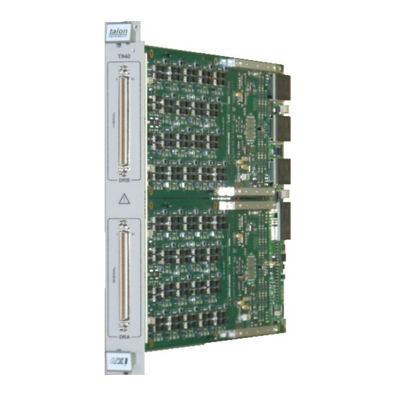
(UUT). Figures 3-1 and 3-2 illustrate the front panel and its connectors. DRB Channel (J201) T940 shown with two Driver/Receiver boards installed (DRA and DRB). DRA Channel (J200) Figure 3-1: T940 Front Panel (Appearance Typical) Astronics Test Systems DRM Front Panel 3-1... -
Page 61: J200 And J201 Dra Channel I/O
PWR Connector – DRA/DRB Power and Signals The PWR connector is an option on the T940 which is used to supply external power to DR3e Driver/Receiver boards and can be used to supply DRM Front Panel 3-2 Astronics Test Systems... -
Page 62: Front Panel Connectors
DRB GND DRA V- Front Panel Connectors Table 3-2 lists the manufacturer’s part numbers and the Astronics Test Systems ordering numbers for the DRM mating connectors. Table 3-3 lists the part and ordering numbers for the DRM cable assemblies. Table 3-2: Mating Connector Part Numbers Connector Manufacturer &... -
Page 63: Front Panel Lbus Lockout Keys
C-type key (PN 455541) for the leftmost module as long as the jumper block for the module is NOT in the Primary position (and it shouldn’t be if it’s the leftmost T940 DRM). DRM Front Panel 3-4 Astronics Test Systems... -
Page 64: Lbus Lockout Key Installation
To secure the lockout keys to the module: 1. Align the lockout keys screw holes with the holes in the module front panel. Astronics Test Systems DRM Front Panel 3-5... - Page 65 2. Install two screws in the holes at the top of the module front panel and tighten the screws. 3. Move the ejector handle to the ejected position, and install a third screw in the hole now made accessible. DRM Front Panel 3-6 Astronics Test Systems...
-
Page 66: Chapter 4
Model T940 User Manual Chapter 4 Functional Description This section describes the DRM hardware block diagrams. For information about DRM address maps and register descriptions, contact your local sales representative or contact Sales Support at atsinfo@astronics.com. Digital Board (DB) FRONT CH[1:32] PANEL... -
Page 67: Vxi Bridge
There are three types of power converters, each of which has seven voltage ranges. Front end features of the DR3E, DR9 and UR14 have headroom requirements to the V+ and V- bias voltages. Refer to the specific front end appendix for Functional Description 4-2 Astronics Test Systems... -
Page 68: Type 1 And Type 3
-4.5V -2 to +14 +21.6V Inter-Module Control The T940 inter-module configuration is determined by jumpers and the primary to terminator order is right to left. The following sections describe the T940 inter- module implementation. Astronics Test Systems Functional Description 4-3... -
Page 69: Terms Used In This Section
64 channels. Driver/Receiver A Driver/Receiver B Data Sequencer A Data Sequencer B Coupled Used to describe a DRM sequencer that is included in a DRS chain. Functional Description 4-4 Astronics Test Systems... -
Page 70: Description
T940 Inter-Module Mode Settings The VXIplug&play API function that sets the inter-module mode is “tat964_setModuleInterconnect”. The valid settings with reference to figure 4-3 are: Astronics Test Systems Functional Description 4-5... - Page 71 DSA and DSB are coupled to a DRS. Terminator DRM Inter-Module Modes: The following modes apply to a DRM that is jumpered as a Terminator. • Independent Not Linked – SIMA set to IMA and SIMB set to IMB. IMJMPR Functional Description 4-6 Astronics Test Systems...
-
Page 72: Examples
Module T940 Inter-Module Mode DRM1 Primary Linked DRM2 Secondary DSA and DSB Coupled DRM3 Secondary DSA and DSB Coupled DRM4 Secondary DSA and DSB Coupled DRM5 Secondary DSA and DSB Coupled DRM6 Terminator Linked Astronics Test Systems Functional Description 4-7... - Page 73 DRS (368 channels). Three Groups of 128 Channels Module T940 Configuration Primary Linked Terminator DSA and DSB Coupled Primary Linked Terminator DSA and DSB Coupled Primary Linked Terminator DSA and DSB Coupled Functional Description 4-8 Astronics Test Systems...
- Page 74 Two Groups of 128 Channels, One Group of 64 Channels, and Two Groups of 32 Channels Module T940 Configuration Primary Linked Terminator DSA and DSB Coupled Primary Linked Terminator DSA and DSB Coupled Secondary Linked Terminator Not Linked Astronics Test Systems Functional Description 4-9...
-
Page 75: Data Sequencer
PRB DATA AUX DATA AUX EN & PATTERN AUX RH PATADDR PCODE PROBE AUX RL1 CONTROL MPSIG RECADDR CH IN/ERR IN RECORD RAM FREQUENCY SYNTHESIZER SEQUENCE CBUS CONTROL CONTROL Figure 4-4: Data Sequencer Block Diagram Functional Description 4-10 Astronics Test Systems... -
Page 76: Terms Used In This Section
IMSEQ Inter-module sequence Controller signals that can be assigned to the VXI or LTB for DRS coupling. Error Pass Valid Sequence Reset DRS Sync Driver Disable Master Reset JUMP Sequence trigger used conditional jumping. Astronics Test Systems Functional Description 4-11... - Page 77 Pause Trigger 1 Pause Trigger 1 Resume Pause Trigger 2 Pause Trigger 2 Resume Phase 1 Resume Phase 2 Resume Phase 3 Resume Phase 4 Resume Execute Start Execute Stop Jump 1 Jump 2 Jump 3 Functional Description 4-12 Astronics Test Systems...
-
Page 78: Sequence Logic
PAT DEL[1:2] PHASE CH IN AUX I/O COUNTER/ TIMER PULSE 250MHz GENERATOR VXICLK10 Figure 4-5: Sequencer Logic Block Diagram Master Clock This block selects the master clock signal used by the timing and waveform generator. Astronics Test Systems Functional Description 4-13... -
Page 79: System Clock
This block contains the Watchdog, Sequence Timeout, Pattern Delay (2) and the Pattern Timeout Timers. Probe/Flag RAM The probe input code, probe results and CONDEN/BERREN data for each pattern is stored in this RAM. Functional Description 4-14 Astronics Test Systems... -
Page 80: Pattern Ram
Multi-purpose signal (MPSIG) which can be combined with other signals on the Driver/Receiver board and provided to the user on the power connector. Probe expect data is received from the Probe/Flag RAM and result data is generated that is stored back into the Probe/Flag RAM. Astronics Test Systems Functional Description 4-15... -
Page 81: Driver/Receiver
The DRM can accommodate two Driver/Receiver boards (named DRA or DRB for their mounted location). Each Driver/Receiver board contains unique driver/receiver circuitry and front panel connector pinouts that are described in an appendix dedicated to each specific Driver/Receiver type. Functional Description 4-16 Astronics Test Systems... -
Page 82: Chapter 5
(DRS). Each 32 channel group in the DRM can be included in the DRS or it can be independent. Up to eight DRMs can be coupled. The SFP is a DRM utility that can be used to debug or check out user configurations and programming. Astronics Test Systems Soft Front Panel Operation 5-1... -
Page 83: Sfp Main Panel
The following warning will display if a DRM module with a type 3 power converter is installed in a VXI 3.0 chassis. Figure 5-2: Initialize Warning SFP Main Panel After a VXI session has opened and the reset option selected, the main panel is displayed. Soft Front Panel Operation 5-2 Astronics Test Systems... -
Page 84: Figure 5-3: Main Panel
Publication No. 980938 Rev. K Model T940 User Manual Title Menu Company Chassis Logo Data Active Module Module Data Data Figure 5-3: Main Panel Figure 5-4: Main Panel UR14 Astronics Test Systems Soft Front Panel Operation 5-3... -
Page 85: Company Logo
DRM that the SFP is connected to. Module Data The module data is displayed in four separate controls. The module data is stored in non-volatile memory. Title Bar The title bar will display the current project file. Soft Front Panel Operation 5-4 Astronics Test Systems... -
Page 86: Sfp Main Panel Menu Bar
Description Clears the DRM hardware to power up reset settings [tat964_reset] Open Opens a file browser for choosing a configuration file. The chosen file is loaded and displayed on the title bar Astronics Test Systems Soft Front Panel Operation 5-5... -
Page 87: Config Menu
Displays the panel for programming module parameters Data Sequencer A Displays the panel for programming DSA parameters Data Sequencer B Displays the panel for programming DSB parameters Channels Displays the panel for programming channel parameters Soft Front Panel Operation 5-6 Astronics Test Systems... -
Page 88: Edit Menu
The Execute Menu is used to program the run option and run the sequences. Figure 5-10: Execute Menu Table 5-4: Execute Menu Descriptions Menu Option Description Displays the execution panel for DSA Displays the execution panel for DSB Astronics Test Systems Soft Front Panel Operation 5-7... -
Page 89: Instrument Menu
Chip Displays the chip temperature panel Temperature Help Menu The Help Menu is used to open the instrument driver help contents and display the SFP programming information panel. Figure 5-12: Help Menu Soft Front Panel Operation 5-8 Astronics Test Systems... -
Page 90: Opening A Vxi Drm Session
DRMs have been identified, a selector panel will display (only if more than one DRM is found). Selecting one of the modules opens a VXI session with that module and then displays the main panel. Astronics Test Systems Soft Front Panel Operation 5-9... -
Page 91: Configuring The Global Hardware Parameters
Access this panel from the menu bar: Config > Module. The Configure Module panel is used to program the inter-module mode, power converter mode/state, Linked Trigger bus routing, signal delays, VXI TRG routing, driver/receiver properties, and record settings. Soft Front Panel Operation 5-10 Astronics Test Systems... -
Page 92: Inter-Module Mode
Primary and Terminator module. Two Independent modes are available: 1. Independent Not Linked- DSA and DSB are not linked together. 2. Independent Linked - DSA and DSB are linked. Astronics Test Systems Soft Front Panel Operation 5-11... -
Page 93: Table 5-8: Inter-Module Mode Settings
DSB Control DRM Type Independent Not Linked Independent Independent Linked Independent Primary DSA Coupled Primary Primary DSA and DSB Coupled Primary Secondary Not Linked Secondary Secondary Linked Secondary Secondary DSA Coupled Secondary Soft Front Panel Operation 5-12 Astronics Test Systems... -
Page 94: Power Converter
The pull down control is disabled (dimmed) for DR installed power converters. The relevant VXIplug&play API functions are: • tat964_setPowerConverter • tat964_setPowerConverterState Linked Trigger Bus The Linked Trigger Bus (LTB) signals are used to pass signals between DSA and DSB. Astronics Test Systems Soft Front Panel Operation 5-13... -
Page 95: Ltbn Signal
Sequence active flag Error DRM error flag Pass Valid DRM Pass Valid signal Waveform 5 Waveform 5 DRM Sync DRM Sync signal Driver Disable DRM driver disable command Waveform 6 Waveform 6 Soft Front Panel Operation 5-14 Astronics Test Systems... -
Page 96: Invert
This command button displays the group configuration panel and is only valid for group enabled front end modules like the DR4. Figure 5-17: Configure Group Panel Group Attributes This table control programs the following group attributes. Astronics Test Systems Soft Front Panel Operation 5-15... -
Page 97: Offset
The group state must be off to update this attribute and all group IO levels are set to 0V. The relevant VXIplug&play API function is: • tat964_setGroupMinMax Slew The group slew specifies the slew of the group channels. The selections for this pull-down control are: Soft Front Panel Operation 5-16 Astronics Test Systems... -
Page 98: Oc Src
• Offset • IO Min • IO Max When enabled (un-dimmed) this button programs the offset, IO min and IO max group attributes. The relevant VXIplug&play API function is: • tat964_setGroupAttribute Astronics Test Systems Soft Front Panel Operation 5-17... -
Page 99: Group [1
This command button displays the “Set VXI Triggers” panel so the TTLTRG and ECLTRG signals can be programmed for the selected sequencer. The panel contains a pull-down control and Invert button for each TTLTRG/ECLTRG signal. Soft Front Panel Operation 5-18 Astronics Test Systems... -
Page 100: Ttltrg And Ecltrg Signal
This pull-down control programs the signal source for the specified VXI trigger. The selections for this pull-down control are: Table 5-15: Signal Pull-Down Settings Setting Description of the VXI Trigger Source Signal None Disables the TTLTRG driver Astronics Test Systems Soft Front Panel Operation 5-19... -
Page 101: Invert
The relevant VXIplug&play API functions are: • tat964_setTtlTriggers • tat964_setEclTriggers D/R Properties This command button displays the “Configure DSn D/R Properties” panel so the configuration settings can be programmed for applicable Driver/Receiver boards. Soft Front Panel Operation 5-20 Astronics Test Systems... -
Page 102: Dut_Gnd
+10V ranges on Type 1 and 3 Power Converters and except for the -15V to +2V and -10V to +9V ranges on the Type 4 Power Converter. Refer to specific Driver/Receiver board specifications for voltage range levels. Astronics Test Systems Soft Front Panel Operation 5-21... -
Page 103: Mfsig Source
Sequence Timeout MPSIG goes high when the sequence timeout is true. Pattern Timeout MPSIG goes high when the pattern timeout is true. Sync Error MPSIG goes high when the sync error is true. Soft Front Panel Operation 5-22 Astronics Test Systems... -
Page 104: Error Pulse Width
Count (see the section on Step Record Mode later in this chapter). Note: If Step Record Mode is set to either Record Error or Record Response, then the Record Mode setting will be ignored. The selections for this pull-down control are: Astronics Test Systems Soft Front Panel Operation 5-23... -
Page 105: Config Data Sequencer A/B
Figure 5-20: Configure Data Sequencer Configure Clocks Access this panel from the menu bar: Config > Data Sequencer x> Clocks. (Where “x” is the sequencer you wish to configure.) Soft Front Panel Operation 5-24 Astronics Test Systems... -
Page 106: Master Clock
48 MHz. Using the 500 MHz clock with 21 counts yields a data rate of 47.619 MHz, the closest pattern rate achievable using the 500 MHz clock. The relevant VXIplug&play API function is: • tat964_setMasterClockSource Astronics Test Systems Soft Front Panel Operation 5-25... -
Page 107: System Clock
Divide the external signal by two and use the rising edge as the active Rising Edge edge Divide by 2 Divide the external signal by two and use the falling edge as the active Falling Edge edge Soft Front Panel Operation 5-26 Astronics Test Systems... -
Page 108: External Offset
The valid external reference frequency range is from 5 MHz to 80 MHz. The relevant VXIplug&play API function is: • tat964_setFreqSynth Astronics Test Systems Soft Front Panel Operation 5-27... -
Page 109: Configure Timers
Sequence Step that has a conditional loop where one is waiting for a termination condition to proceed to the next Sequence Step: • There is a global enable. • It starts when the first branch takes place. Soft Front Panel Operation 5-28 Astronics Test Systems... -
Page 110: Watchdog Action
Set bit in event register only when a watchdog timeout occurs. Disable Drivers Set bit in event register and disable the drivers when a watchdog timeout occurs. The relevant VXIplug&play API function is: Astronics Test Systems Soft Front Panel Operation 5-29... -
Page 111: Watchdog Time
This numeric control is used to specify the pattern timeout count. The timeout is programmed in 10 ns steps with a range of 20 ns to 42.949672970 s. The relevant VXIplug&play API function is: Soft Front Panel Operation 5-30 Astronics Test Systems... -
Page 112: Pattern Delay 1-2
If the pattern timing is paused by either the assert or return edge of a phase, then this trigger is used to resume the timing. Halt Trigger The halt trigger causes the sequencer to halt based on the current halt mode. Astronics Test Systems Soft Front Panel Operation 5-31... -
Page 113: Trigger
Jump 4 Select Jump 4 to edit Note: See the Jumping, Halting, Counting and Logging Errors section of Chapter 8 for a more in-depth explanation. Source This pull-down control programs the trigger source. Soft Front Panel Operation 5-32 Astronics Test Systems... -
Page 114: Test Condition
Test for a low level High Level Test for a high level Rising Edge Test for a rising edge Falling Edge Test for a falling edge The relevant VXIplug&play API functions are: • tat964_setHandshakePauseTrigger • tat964_setHandshakeResumeTrigger Astronics Test Systems Soft Front Panel Operation 5-33... -
Page 115: Input Mode
Table 5-32 Trigger Event Clear Settings Setting Description Start Clear flip-flops at start of burst Step Clear flip-flops at start of every sequence step Event True Clear flip-flops when trigger event tests true Soft Front Panel Operation 5-34 Astronics Test Systems... -
Page 116: Configure Pulse Generator
This toggle control is used to program the pulse generator resolution to either 10 ns or 20 ns. The relevant VXIplug&play API function is: • tat964_setPulseParameters Mode This pull-down control programs the pulse generator mode. Astronics Test Systems Soft Front Panel Operation 5-35... -
Page 117: Step
This input control is used to specify the pulse generator delay from the start of the sequence or sequence step. Delay is not applicable when the Pulse Generator is in Continuous mode. Soft Front Panel Operation 5-36 Astronics Test Systems... -
Page 118: Width
The relevant VXIplug&play API function is: • tat964_setPulseWidth Configure Data Sequencer Settings Access this panel from the menu bar: Config > Data Sequencer x> Settings. (Where “x” is the sequencer you wish to configure.) Astronics Test Systems Soft Front Panel Operation 5-37... -
Page 119: Error Record Basis
The relevant VXIplug&play API function is: • tat964_setRecordParameters Record Offset The record offset allows the user to shift the record signals (pattern code expect and mask, record offset, window strobes) to accommodate system and UUT Soft Front Panel Operation 5-38 Astronics Test Systems... -
Page 120: Record Type
DRMs/Sequencers via the TTL/ECL or Linked TRG bus respectively. The ECL TRG Bus is recommended for data rates greater than 10 MHz. This is discussed in more detail in the Jumping, Halting, Astronics Test Systems Soft Front Panel Operation 5-39... -
Page 121: Error Address Basis
The selections for this pull-down control are: Table 5-39: Timing Mode Settings Setting Description Per Step Multi 1024 steps with four phase/window pairs per step. Per Step Single 4096 steps with one phase/window pair per step. Soft Front Panel Operation 5-40 Astronics Test Systems... -
Page 122: Output-To-Input Disable
DRMs/Sequencers via the TTL/ECL or Linked TRG. The ECL TRG Bus is recommended for data rates greater than 10 MHz. This is discussed in more detail in the Jumping, Halting, Counting and Logging Errors sections in Astronics Test Systems Soft Front Panel Operation 5-41... -
Page 123: Pass Valid Mode
The selections for this pull-down control are: Table 5-42: Pass Valid Mode Settings Setting Description Disable Do not use pass valid signal Enable Use pass valid signal The relevant VXIplug&play API function is: • tat964_setPassFailParameters Soft Front Panel Operation 5-42 Astronics Test Systems... -
Page 124: Over-Current
The selections for the over-current window pull-down controls are: Astronics Test Systems Soft Front Panel Operation 5-43... -
Page 125: Drive Fault
If an output pin is enabled to also compare its state (Capture mode programmed and compare levels set), then a drive fault will be generated if the compare level does not match the output state. Drive faults can be used with stimulus only Soft Front Panel Operation 5-44 Astronics Test Systems... -
Page 126: Probe
The probe module connects to the UR14 J1A connector. Figure 5-27: Probe Panel Probe State This control initializes/resets the probe resources on the UR14 module. Note: Disable the Probe State when not in use. See the Jumping, Halting, Astronics Test Systems Soft Front Panel Operation 5-45... -
Page 127: Offset
The capture CRC mode allows the user to select the capture signal for the probe CRC. The selections for this pull-down control are: Table 5-46: CRC Capture Settings Setting Description Disable Disable Probe CRC Capture Soft Front Panel Operation 5-46 Astronics Test Systems... -
Page 128: Probe Button
AUX1 A on the UR14 Driver/Receiver board. The relevant VXIplug&play API function is: • tat964_setProbeConnect Probe Input Compare High and Low These two controls set the probe input high and low comparator levels. The Astronics Test Systems Soft Front Panel Operation 5-47... -
Page 129: Probe Cal Connect
PROBE OUT signal on the UR14 Driver/Receiver board. The relevant VXIplug&play API function is: • tat964_setProbeConnect Compensation This control initiates a compensation calibration. The user is prompted to connect the probe to the calibration BNC. Soft Front Panel Operation 5-48 Astronics Test Systems... -
Page 130: Dc Cal
This control initiates a DC level calibration. The user is prompted to connect the probe to the calibration BNC. After calibration has been perfomed, the user is prompted to update the EEPROM. The relevant VXIplug&play API function is: Astronics Test Systems Soft Front Panel Operation 5-49... -
Page 131: Attributes
3. External phase 3 mode uses the Jump 1 trigger to generate the phase 3 signal. Phase 3 is typically set to Jump 1 to perform a Phase Replacement during a Pause and Resume operation. The selections for this pull-down control are: Soft Front Panel Operation 5-50 Astronics Test Systems... -
Page 132: Window 3 Mode
The valid delay range is from 0 to 15 with 2ns resolution. The relevant VXIplug&play API function is: • tat964_setSequencerAttribute CRC Preload This control sets the seed number for the CRC preload and are available in sequencer revision 0.23 and later. Astronics Test Systems Soft Front Panel Operation 5-51... -
Page 133: Crc Algorithm And Capture Mask
Sequencer revisions 0.21 and later have dedicated static timing and do not require the pulse generator. Thus, the pulse generator is available for user settings. The selections for this pull-down control are: Soft Front Panel Operation 5-52 Astronics Test Systems... -
Page 134: Configuring The I/O Channels
Access this panel from the menu bar: Config > Channels. Figure 5-29: Configure Channels Panel Selecting the Channels Before the channel parameters or properties can be programmed, the channels must be selected. There are two methods for selecting the channels: Astronics Test Systems Soft Front Panel Operation 5-53... -
Page 135: Channel Parameters
Use phase 2 timing signal to control output driver timing. Phase 3 Use phase 3 timing signal to control output driver timing. Phase 4 Use phase 4 timing signal to control output driver timing. Soft Front Panel Operation 5-54 Astronics Test Systems... -
Page 136: Stimulus Format
Phase Assert – Output driver goes to level determined by the Pattern Code instruction in Pattern Memory. • Phase Return – Output driver goes to complemented level determined by the Pattern Code instruction in Pattern Memory Astronics Test Systems Soft Front Panel Operation 5-55... -
Page 137: Capture Signal
V+/V- in the Execute Panel Modes and Settings section of this chapter). The relevant VXIplug&play API function is: • tat964_setChannelParameters Capture Signal This pull-down control programs the selected channel(s) capture signal. The selections for this pull-down control are: Soft Front Panel Operation 5-56 Astronics Test Systems... -
Page 138: Capture Mode
When the channel is returned from Static to Dynamic Mode, dynamic operation will resume as though it had never been put into the Static Mode. The selections for this pull-down control are: Astronics Test Systems Soft Front Panel Operation 5-57... -
Page 139: Properties
Driver/Receiver board does not support a property and you select it, a Soft Front Panel Error message box, similar to the following, appears. Click Ignore to clear the error and return to the control panel. Soft Front Panel Operation 5-58 Astronics Test Systems... -
Page 140: Driver Levels
Note: The external supply voltages will also need to be adequate for the desired drive levels when using the DR3e with external power option. The relevant VXIplug&play API function is: Astronics Test Systems Soft Front Panel Operation 5-59... -
Page 141: Comparator Levels
• tat964_setChannelSourceParameters Termination This allows the user to set the termination as direct or series. See specific Driver/Receiver board appendix for termination values. The relevant VXIplug&play API function is: • tat964_setChannelSourceParameters Soft Front Panel Operation 5-60 Astronics Test Systems... -
Page 142: Over-Current Alarm Levels
Fixed resistive load Resistive to VCC+GND Fixed resistive load The programmable current load allows the user to specify a source and sink current load and a commutating voltage (VCOM). Note: VCC=3.3V for the DR1. Astronics Test Systems Soft Front Panel Operation 5-61... -
Page 143: Figure 5-31: Current Load
Resistive load set to 165 Ω Resistive load set to 207 Ω Resistive load set to 240 Ω Resistive load set to 290 Ω Resistive load set to 540 Ω Resistive load set to 1040 Ω 1040 Soft Front Panel Operation 5-62 Astronics Test Systems... -
Page 144: Channel Connect
This allows the user to add delay to the comparator inputs for DR3e, DR9, and UR14 front end channels. The range for Comparator Delay is from -1 (bypass delay) to 31 (~19.35ns) 625ps per count. Astronics Test Systems Soft Front Panel Operation 5-63... -
Page 145: Channel Mode
The relevant VXIplug&play API function is: • tat964_setChannelMode Configure UR14 Channel Properties The UR14 channel settings consist of a single threshold compare level and an over current detect level programmed in groups of eight channels. Soft Front Panel Operation 5-64 Astronics Test Systems... -
Page 146: Compare Input (V)
Sets the compare input and OC detect levels of all four channel groups to the current panel settings. The relevant VXIplug&play API functions are: • tat964_setUtilitySenseLevel • tat964_setUtilitySourceParameter Configuring the AUX Channels Access this panel from the menu bar: Config > AUX Outputs. Astronics Test Systems Soft Front Panel Operation 5-65... -
Page 147: Figure 5-34: Configure Aux Channels Panel
The AUX channels are a set of 12 multi-purpose signals that can be used for any of the following I/O resources: 1. Trigger Source Input 2. Frequency Synthesizer Reference Clock Input 3. System Clock Input Soft Front Panel Operation 5-66 Astronics Test Systems... -
Page 148: Table 5-64: Drn Aux Configuration
AUX1 A, AUX2 A Programmable Used for probe input (AUX1) and probe cal (AUX2) AUX3 A, AUX4 A LVTTL AUX4 used for probe compensation. AUX5 A LVTTL Shares front panel pin with AUX9 A Astronics Test Systems Soft Front Panel Operation 5-67... -
Page 149: Configuring The Aux/Uaux Signals
AUX number. Refer to the specific Driver/Receiver board appendix for AUX capabilities. All AUX and UAUX signals share the controls listed in the following figure: Figure 5-36: Shared AUX/UAUX Controls Soft Front Panel Operation 5-68 Astronics Test Systems... -
Page 150: State
SEQ_CLK_D_In Test signal T0CLK Out Test signal SEQ_CLK Out Test signal Jump Out Test signal SEQ_CLK_D_Out Test signal Pulse Generator Pulse generator signal Record Active 1 = Active, 0 = Not Active. Astronics Test Systems Soft Front Panel Operation 5-69... -
Page 151: Input Bus Source
Table 5-68: Input Bus Select Source Settings Setting Description AUX1 Good 0 Source set to AUX1 Good zero signal. AUX1-12 Good 1 Source set to AUXn Good one signal. CHT1 Source set to channel test 1 Soft Front Panel Operation 5-70 Astronics Test Systems... -
Page 152: Connect State
AUX configured as bipolar ECL. Differential AUX configured as differential ECL The relevant VXIplug&play API function is: • tat964_setAuxEclMode Logic Mode (LVTTL/Bipolar ECL Logic) This control allows the user to select the LVTTL/ECL mode. Astronics Test Systems Soft Front Panel Operation 5-71... -
Page 153: Configuring The Interrupts
The events that can generate an interrupt depend on the specific hardware installed. The Digital Board can generate these two events: 1. CPU Interrupt 2. Sequencer FPGA Temperature Alert Access this panel from the menu bar: Config > Interrupts. Soft Front Panel Operation 5-72 Astronics Test Systems... -
Page 154: Condition
The relevant VXIplug&play API function is: • tat964_setInterruptMode Event This control indicates that the event is currently true. The relevant VXIplug&play API function is: • tat964_queryInterruptEvent Astronics Test Systems Soft Front Panel Operation 5-73... -
Page 155: Editing The Data Sequencers
The Return signal is not used for the Non Return format code. (See Stimulus Format earlier in this chapter.) Phase 1 Phase 2 Pattern Period Figure 5-39: Phase Timing Soft Front Panel Operation 5-74 Astronics Test Systems... -
Page 156: Figure 5-40: Data Sequencer Timing Sets Panel
Per Step Single - 4096 timing sets with one phase/window group per timing set. TS0 is the timing for sequence step 1, TS1 is the timing for sequence step 1, … , timing set 4095 is the timing for sequence step 4095. Astronics Test Systems Soft Front Panel Operation 5-75... -
Page 157: Timing Set Value Rules
(CPP > 1) are programmed. (See Clocks per Pattern later in this chapter.) Advanced Timing Set Features Two advanced timing set features are available: 1. Phase/Window Spanning Soft Front Panel Operation 5-76 Astronics Test Systems... -
Page 158: Phase/Window Spanning
(See Patterns in Chapter 5.) Access this panel from the menu bar: Edit > Data Sequencer x > Patterns. (Where “x” is the sequencer you wish to configure.) Astronics Test Systems Soft Front Panel Operation 5-77... -
Page 159: Append
The offset can be from 0 to 262140 and must be a multiple of four. The relevant VXIplug&play API functions are: • tat964_queryPatternSet • tat964_queryPatternSetList Append This control allows the user to append more patterns to the selected pattern set. Soft Front Panel Operation 5-78 Astronics Test Systems... -
Page 160: Assign
Press the Close command button to exit the panel without any changes. The relevant VXIplug&play API function is: • tat964_appendPattern Assign This control allows the user to assign a new size and/or offset to the selected pattern. Astronics Test Systems Soft Front Panel Operation 5-79... -
Page 161: Edit Data
This control displays the view/edit pattern set panel. This panel allows the user to view/edit the contents of the pattern set memory. Double-clicking on the desired pattern set can also open this panel. Soft Front Panel Operation 5-80 Astronics Test Systems... -
Page 162: Figure 5-44: Pattern Set Sequencer Data Panel
The pattern codes are described in Figure 5-47 and Table 5-TTT. The pattern set is displayed in pages of 32 patterns. The View menu bar lists the page control shortcuts listed below: Figure 5-45: Pattern Set Data – View Menu Astronics Test Systems Soft Front Panel Operation 5-81... -
Page 163: Figure 5-46: Goto Pattern Panel
Burst Error, Burst Error counting and the logging of errors in the Error Address Memory. 2. CONDEN – Condition Enable. This flag allows the user to designate which patterns will be considered for PASS/FAIL jump tests. Soft Front Panel Operation 5-82 Astronics Test Systems... -
Page 164: Figure 5-48: Probe Codes
Publication No. 980938 Rev. K Model T940 User Manual The row labeled “PROBE” displays the probe expect code for each pattern. There are thirty four probe expect codes: Figure 5-48: Probe Codes Astronics Test Systems Soft Front Panel Operation 5-83... -
Page 165: Table 5-71: Probe Expect Codes
RH three or more times and ends above Signal starts below RL, crosses RL three or more times, RH two or more times and ends between RL and RH. LGRE Signal starts below RL, crosses the RL Soft Front Panel Operation 5-84 Astronics Test Systems... - Page 166 RH two or more times and ends between RL and RH. The rows labeled CH1 through CHn contain the pattern codes for the specified channels. There are fourteen pattern codes. The following table lists how each Astronics Test Systems Soft Front Panel Operation 5-85...
-
Page 167: Figure 5-49: Pattern Set Data - File Menu
The relevant VXIplug&play API functions are: • tat964_setPatternData • tat964_setPatternTestEnable • tat964_setProbeExpectData The pattern data can be imported/exported using the File menu bar selection. Figure 5-49: Pattern Set Data – File Menu The import/export formats include: Soft Front Panel Operation 5-86 Astronics Test Systems... -
Page 168: Import/Export File Format
ASCII Hex The ASCII hex format represents pattern data as viewable ASCII hex characters, one character per channel. The following table lists the pattern code to ASCII/Binary value translation. Astronics Test Systems Soft Front Panel Operation 5-87... -
Page 169: Table 5-73: Ascii/Binary Data Format
Bit15, Bit 14 Code ‘a’ ‘b’ ‘c’ ‘n’ Probe Expect Bit 13 through Bit ‘a’ ‘b’ ‘c’ • • • • • • ‘y’ ‘z’ ‘0’ ‘1’ ‘2’ ‘3’ ‘4’ ‘5’ ‘6’ Soft Front Panel Operation 5-88 Astronics Test Systems... -
Page 170: Binary
The flag code for each pattern requires two bits. Bits 15 and 14 contain the flag code and bits 13 through 8 contain the probe expect code.. Table 5-44 lists the binary value/pattern code translation. Astronics Test Systems Soft Front Panel Operation 5-89... -
Page 171: Ascii String
All waveforms can be output on any AUX I/O Channel. Waveform 1 and Waveform 3 can also be output on any channel. Access this panel from the menu bar: Edit > Data Sequencer x> Waveforms. Soft Front Panel Operation 5-90 Astronics Test Systems... - Page 172 (Where “x” is the sequencer you wish to configure.) Figure 5-50: Edit Waveforms Panel Waveform 1 Figure 5-51: Edit Waveforms Panel Waveform 5 Table Size This pull-down control programs the waveform table size for waveforms 1-4. Astronics Test Systems Soft Front Panel Operation 5-91...
-
Page 173: Waveform
3 Transitions at 5, 10, 15; Would generate the following waveform; "00000111110000011111111..." Bits 1-5 low Bits 6-10 high Bits 11-15 low Bits 16 through the size of the table high. Example 2: Beginning Level = 1; Soft Front Panel Operation 5-92 Astronics Test Systems... -
Page 174: Editing Sequence Parameters
These controls program the loop counter mode. There are sixteen 16-bit loop counters. Each of the sixteen loop counters can be programmed to either reload its count or disable when the terminal count is reached. Astronics Test Systems Soft Front Panel Operation 5-93... -
Page 175: Pipeline
Sets the closing edge of window 1 as the vector strobe. Window 2 Sets the closing edge of window 2 as the vector strobe. Window 3 Sets the closing edge of window 3 as the vector strobe. Soft Front Panel Operation 5-94 Astronics Test Systems... -
Page 176: Set Vector Bits
Configuring the vector signals consists of the following: 1. Select the Source. 2. Program the Input Mode. Figure 5-53: Edit Vector Bits Panel Source This pull-down control programs the vector bit source. The selections for this pull-down control are: Astronics Test Systems Soft Front Panel Operation 5-95... -
Page 177: Input Mode
Configuring the vector table signal consists of the following: 1. Select the Vector Bit Index 2. Select the Vector Jump Step 3. Program the Timing Set (only used in the indexed timing mode). Soft Front Panel Operation 5-96 Astronics Test Systems... -
Page 178: Vector Bit Index
The expect value is compared to the response high (Good 1) of the input channel. A high in the mask, disables the comparison. The result of all four channel test registers can be routed to the VXI TTL trigger Astronics Test Systems Soft Front Panel Operation 5-97... -
Page 179: Expect
The relevant VXIplug&play API function is: • tat964_setSequenceChannelTest The T940 VXI Backplane Trigger Bus section of Chapter 8 describes how to use Channel Tests to perform a logical OR and logical AND of two or more channels. Soft Front Panel Operation 5-98 Astronics Test Systems... -
Page 180: Editing Sequence Steps
A double-click on any of the step number cells opens a Sequence Step Data panel for that cell. The T964 Sequencer Operation Details section in Chapter 8 provides detailed information on sequencer operation. The relevant VXIplug&play API functions are: • tat964_selectSequenceStep • tat964_initSequenceSteps Astronics Test Systems Soft Front Panel Operation 5-99... -
Page 181: Internal T0Clk
The CPP value determines the number of System Clocks that will be generated for each Pattern Clock. When CPP = 1, then Pattern Clock is equal to System Clock. When CPP = 2, then Pattern Clock is two times the System Clock. Soft Front Panel Operation 5-100 Astronics Test Systems... -
Page 182: Cpp Phase And Window Triggering
This control is only visible when the sequencer timing mode is set to indexed (see Timing Mode in Chapter 5). The valid values for control are from 0 to 255. The relevant VXIplug&play API function is: • tat964_setSequenceTimingSet Astronics Test Systems Soft Front Panel Operation 5-101... -
Page 183: Last Step
The Gosub Return flag set true will force the sequence step number to be one more than the saved step number. For example, if step number 5 and 7 had a Soft Front Panel Operation 5-102 Astronics Test Systems... -
Page 184: Jump Step
Step Not PASS Jump if the PASS/FAIL flag is NOT a PASS (i.e. FAIL or Indeterminate) Step Not FAIL Jump if the PASS/FAIL flag is NOT a FAIL (i.e. PASS or Indeterminate) Astronics Test Systems Soft Front Panel Operation 5-103... -
Page 185: Loop Count
65536. A count qualified jump only allows the jump to occur a maximum of “count” times. This allows single or multiple steps to be looped. The relevant VXIplug&play API function is: • tat964_setSequenceJump Soft Front Panel Operation 5-104 Astronics Test Systems... -
Page 186: Loop Counter
The relevant VXIplug&play API function is: • tat964_setSequencePassFailClear Step Record Mode This control programs the Step Record Mode during this step. The T940 contains three memories that store error data from a sequence Astronics Test Systems Soft Front Panel Operation 5-105... -
Page 187: Timing
The relevant VXIplug&play API function is: • tat964_setSequenceRecordMode Timing This command button displays the Edit Timing Set panel so the phase and window settings can be programmed for the selected sequencer step (see Soft Front Panel Operation 5-106 Astronics Test Systems... -
Page 188: Patterns
-1, the driver automatically increments the offset to the next higher multiple of 4 from the previous offset. Any other number between 0 and 262140, in multiples of 4, sets the offset. Click Apply to initialize the patterns or Close to cancel. Astronics Test Systems Soft Front Panel Operation 5-107... -
Page 189: Figure 5-59: Initialize Step Pattern Set Panel
If the Patterns control reads a number greater than zero, then this command button displays the Edit Pattern Data panel (see Editing the Patterns Chapter 5). Figure 5-60: Edit Pattern Set Panel Soft Front Panel Operation 5-108 Astronics Test Systems... -
Page 190: Properties
Pause Signal This pull-down control programs the Handshake Pause signal. The selections for this pull-down control are: Table 5-82: Handshake Pause Signal Setting Pause Signal Resume Signal None Handshake mode disabled Astronics Test Systems Soft Front Panel Operation 5-109... -
Page 191: Resume Modifier
Pattern Timeout: Set the pattern timeout (PTO) flag if the specified resume signal is not received by the time the Pattern Timeout timer has exhausted (the Pattern Timeout timer started when the Pause signal was Soft Front Panel Operation 5-110 Astronics Test Systems... -
Page 192: Waveform Properties
Phase output rate being at a multiple of the System Clock period if CPP>1 (PER = PER * CPP). PCLK SCLK The relevant VXIplug&play API function is: • tat964_setSequencePhaseTrigger Astronics Test Systems Soft Front Panel Operation 5-111... -
Page 193: Execute The Sequence
Access this panel from the menu bar: Execute > DSx. (Where “x” is the sequencer you wish to execute.) Figure 5-62: Executing a Sequence Panel The following sections describe the execution overview as well as the indicators and controls of the execute panel. Soft Front Panel Operation 5-112 Astronics Test Systems... -
Page 194: Execution Overview
4. Paused flag: false 5. Active step: 0 6. Pattern Memory: Free STANDBY 1. Idle Active: false “last step/stop (standby finish mode)” 2. Sequence Active: false 3. Halt flag: false 4. Paused flag: false Astronics Test Systems Soft Front Panel Operation 5-113... -
Page 195: Table 5-85: Execute State Transition Description
(also disables output drivers). • execute idle Execute idle sequence Enter step number and depress Execute Idle command button. • execute Execute sequence Enter step number and depress Execute command button. Soft Front Panel Operation 5-114 Astronics Test Systems... -
Page 196: Execute Panel Indicators
When green, indicates that the sequencer is in the IDLE state. The relevant VXIplug&play API function is: • tat964_querySequencerStatus Active LED When green, indicates that the sequencer is in the ACTIVE state. Astronics Test Systems Soft Front Panel Operation 5-115... -
Page 197: Halt Led
Converter Condition register. The relevant VXIplug&play API function is: • tat964_queryPowerConverterCondition D/R Alert Illuminated red indicates that one or more bits are set in the Driver/Receiver event register. The relevant VXIplug&play API function is: Soft Front Panel Operation 5-116 Astronics Test Systems... -
Page 198: Sequence Active
There are ten controls that set the execution mode settings. Start/Arm Selector This slide selects whether the Execute Idle or Execute command buttons arm or start the specified action (See Execute Idle and Execute command button descriptions). Astronics Test Systems Soft Front Panel Operation 5-117... -
Page 199: Channel Drivers
C Error will not shut the V+ and V- off. The relevant VXIplug&play API function is: • tat964_setPowerConnect Execute Idle Step This control sets the idle step number for the Idle command button operation. Soft Front Panel Operation 5-118 Astronics Test Systems... -
Page 200: Execute Step
Sync Pulse 2 is positioned. Pattern Fail Halt the current sequence at the end of the next pattern if the pass/fail flag is set to fail. Astronics Test Systems Soft Front Panel Operation 5-119... -
Page 201: Finish Mode
Go to Idle after sequence completes. The relevant VXIplug&play API function is: • tat964_setFinishSequence Finish Mode Step This control sets the finish mode step number. The relevant VXIplug&play API function is: • tat964_setFinishSequence Soft Front Panel Operation 5-120 Astronics Test Systems... -
Page 202: Stop Mode
This command button displays the Set Sync panel so that Sync 1 and Sync 2 signals can be programmed to generate a pulse. These two sync outputs can be routed to any of the AUX, ECLTRG or TTLTRG Astronics Test Systems Soft Front Panel Operation 5-121... -
Page 203: Sync Number
This control sets the offset from the sync event before the sync pulse starts. The offset can be set from 0 to 1048575 patterns. The relevant VXIplug&play API function is: • tat964_setSyncParameters Soft Front Panel Operation 5-122 Astronics Test Systems... -
Page 204: Length
(single step). See the Pause and Halt section in Chapter 8 for additional details about the use of halt. The relevant VXIplug&play API function is: • tat964_haltSequence Astronics Test Systems Soft Front Panel Operation 5-123... -
Page 205: Resume
Arm PG The Arm PG command button arms the pulse generator. Note: The Pulse Generator will not work in any of its modes until armed. The relevant VXIplug&play API function is: • tat964_armPulseGenerator Soft Front Panel Operation 5-124 Astronics Test Systems... -
Page 206: Stop Pg
Static Data The static data display is accessed from the Execute > DSx > View > Static Data menu bar selection (where “x” is the sequencer you wish to query). Astronics Test Systems Soft Front Panel Operation 5-125... -
Page 207: Stimulus Delay
The delay can be set from Stimulus Delay + 10ns to Stimulus Delay + 40s with 10ns resolution. Note: The Response Delay must be greater than the Stimulus Delay. Soft Front Panel Operation 5-126 Astronics Test Systems... -
Page 208: Stimulus
Response low level. Response high level. Unknown The relevant VXIplug&play API function is: • tat964_queryStaticResponse Kept Data The kept data display is accessed from the Execute > DSx > View > Kept Data Astronics Test Systems Soft Front Panel Operation 5-127... -
Page 209: Results
The relevant VXIplug&play API function is: • tat964_queryKeptPattern Results The Results data display is accessed from the Execute > DSx > View > Results menu bar selection. (Where “x” is the sequencer you wish to query.) Soft Front Panel Operation 5-128 Astronics Test Systems... -
Page 210: View
(.csv). All numeric values are displayed as decimal. CRC Save File Format The CRC results are saved in the following format: Astronics Test Systems Soft Front Panel Operation 5-129... -
Page 211: Error Address Save File Format
Record Data Save File Format The Record Data results are saved in the following format: <header><line feed> <step>,<offset>,<data><line feed> Where: <header> “STEP,OFFSET,RECORD DATA” <step> Step number of the error. <offset> Pattern number. <data> Record Memory contents. Soft Front Panel Operation 5-130 Astronics Test Systems... -
Page 212: Probe Data Save File Format
CRCs can be accumulated for all 32 channels as well as AUX1 which is dedicated for the probe channel (shown at the left). The relevant VXIplug&play API functions are: • tat964_queryCrc • tat964_queryProbeCrc Astronics Test Systems Soft Front Panel Operation 5-131... -
Page 213: Error Address Display
(if Record Type set to Normal) • tat964_queryRecordIndex (if Record Type set to Indexed) The View menu selection allows the address column of the error address panel to toggle between decimal and hexadecimal. Soft Front Panel Operation 5-132 Astronics Test Systems... -
Page 214: Record Index Display
When the record type is set to indexed, the sequence results are stored sequentially in the record memory starting at offset 0. The record index memory allows the user to determine sequence step order that filled the record memory. Astronics Test Systems Soft Front Panel Operation 5-133... -
Page 215: Record Data Display
The record memory display is accessed from the Execute > DSx >View>Results menu bar selection and setting the View control to Record Data. (Where “x” is the sequencer you wish to query.) Soft Front Panel Operation 5-134 Astronics Test Systems... -
Page 216: Probe Data Memory Display
The probe data memory display is accessed from the Execute > DSx > View > Results menu bar selection and setting the View control to Probe Data. (Where “x” is the sequencer you wish to query.) Astronics Test Systems Soft Front Panel Operation 5-135... -
Page 217: Figure 5-75: Probe Data Panel
The combination of the eight bits allows the following probe states: Open Close Open Close Open Close Middle – Signal remains High – Signal remains above Low – Signal remains below between RL and RH. Soft Front Panel Operation 5-136 Astronics Test Systems... - Page 218 Middle Glitch Low - Signal Low Glitch - Signal starts below starts below RL, crosses the RL starts between RL and RH, RL, crosses the RL two or more times and ends below RL. Astronics Test Systems Soft Front Panel Operation 5-137...
- Page 219 RH two or crosses RL two or more times, two or more times and ends more times and ends between RH three or more times and above RH. RL and RH. ends above RH. Soft Front Panel Operation 5-138 Astronics Test Systems...
-
Page 220: Status Indicator Panels
Counter/Timer • Sequencer Events The sequence events display is accessed from the Execute > DSx > View > Sequencer Events menu bar selection. (Where “x” is the sequencer you wish to query.) Astronics Test Systems Soft Front Panel Operation 5-139... -
Page 221: Figure 5-76: Sequencer Event Status Panel
The idle state has been entered Sequence Started The sequence active state has been entered. External Halt One or more external halts occurred. Burst Error One or more errors occurred. Jump One or more jumps occurred. Soft Front Panel Operation 5-140 Astronics Test Systems... - Page 222 ERROR Setup Fault DRS/Linked Error Signal not assigned. PASS VALID Setup DRS/Linked Pass Valid Signal not assigned. Fault Counter Data Ready Frequency counter data ready. Interval Data Ready Interval Timer data ready. Astronics Test Systems Soft Front Panel Operation 5-141...
-
Page 223: Enable
This command button resets the event LEDs. Sequencer Data Panel The sequence status display is accessed from the Execute > DSx > View > Sequencer Data menu bar selection. (Where “x” is the sequencer you wish to query.) Soft Front Panel Operation 5-142 Astronics Test Systems... -
Page 224: Counter Active
This indicator displays the step number that was active when the DRS sync error occurred. The relevant VXIplug&play API function is: • tat964_querySequencerSyncError Sync Error Pattern Address This indicator displays the pattern address that was active when the DRS sync Astronics Test Systems Soft Front Panel Operation 5-143... -
Page 225: Status
Driver/Receiver Events Panel The Driver/Receiver events display is accessed from the Execute > DSx > View > Driver/Receiver Events menu bar selection. (Where “x” is the sequencer you wish to query.) Soft Front Panel Operation 5-144 Astronics Test Systems... -
Page 226: Figure 5-78: Dr3E/Dr9/Ur14 Driver/Receiver (D/R) Events Panel
One or more of the Pin Alert Electronics devices has exceeded the specified temperature. C Error The I2C communication bus has had an error in the communication protocol. Over-voltage One or more channels Fault had an over-voltage. Astronics Test Systems Soft Front Panel Operation 5-145... -
Page 227: Figure 5-79: Dr4 Driver/Receiver (D/R) Events Panel
The -24 V fuse reports open -12V Fault The -12 V fuse reports open VTM Over VTM exceeded output current >3.25A Current and shutdown. Fault VTM High VTM High current warning >2.8A Current Warning Soft Front Panel Operation 5-146 Astronics Test Systems... -
Page 228: Enable
Alert Text This indicator displays the channel that generated the temperature alert event. The alert is returned as a 32 bit number and then converted to text by the soft front panel. Astronics Test Systems Soft Front Panel Operation 5-147... -
Page 229: Driver/Receiver Data Panel
Driver/Receiver Data Panel The Driver/Receiver data display is accessed from the Execute > DSx > View > Driver/Receiver Data menu bar selection. (Where “x” is the sequencer you wish to query.) Soft Front Panel Operation 5-148 Astronics Test Systems... -
Page 230: Figure 5-80: Driver/Receiver Data Panel
The DR3e AUX1 signal is a dual comparator, AUX1L indicates the low comparator and AUX1H indicates the high comparator. The relevant VXIplug&play API functions are: • tat964_querySequencerChannels • tat964_querySequencerAux Astronics Test Systems Soft Front Panel Operation 5-149... -
Page 231: Vxi Trigger Readback Panel
• tat964_queryVxiTrigger Query Power Results Message The query power results display is accessed from the Execute > DSx >View>Power Query menu bar selection. (Where “x” is the sequencer you wish to query.) Soft Front Panel Operation 5-150 Astronics Test Systems... -
Page 232: Power Converter Condition Panel
DRM so the DSA and DSB selection will display the same panel. Figure 5-83: Power Converter Condition Panel The following power converter bits are defined: VTM1 Fault Power converter VTM1 failure. VTM2 Fault Power converter VTM2 failure. Astronics Test Systems Soft Front Panel Operation 5-151... -
Page 233: Counter/Timer Panel
Counter/Timer menu bar selection where x is sequencer A or B. One Counter/Timer is provided for each sequencer. Figure 5-84: Timer/Counter Panel Function This pull-down control programs the counter/timer function. The selections for this pull-down control are: Soft Front Panel Operation 5-152 Astronics Test Systems... -
Page 234: Input <1-3> Source
Freq. Synth. Frequency Synthesizer VXICLK10 10 MHz VXI backplane clock. 250 MHz 500 MHz clock divided by 2. Pulse Generator Pulse Generator. The relevant VXIplug&play API function is: • tat964_setCounterInput • tat964_queryCounterInput Astronics Test Systems Soft Front Panel Operation 5-153... -
Page 235: Input <1-3> Slope
One second gate time. Ten second gate time. The relevant VXIplug&play API function is: • tat964_setCounterAperture • tat964_queryCounterAperture Trigger This pull-down control programs the trigger source. The selections for this pull-down control are: Soft Front Panel Operation 5-154 Astronics Test Systems... -
Page 236: Initiate
Retrieve the results of the selected counter/timer function. The relevant VXIplug&play API function is: • tat964_measureCounterResults PMU Panel The PMU display is accessed from the Execute > DSx >View>PMU menu bar selection. Figure 5-85: PMU Panel Astronics Test Systems Soft Front Panel Operation 5-155... -
Page 237: Channel
The short RAM test tests each RAM at the major address bits locations, i.e., 0, 1, 2, 4, 8, 16 . . . etc. The self-test result codes are: Soft Front Panel Operation 5-156 Astronics Test Systems... -
Page 238: Table 5-106: Self Test Result Code Descriptions
DSB pattern 1 (CH9-CH16) RAM test failed DSB pattern 2 (CH17-CH24) RAM test failed DSB pattern 3 (CH25-CH32) RAM test failed DSB record RAM test failed DSB probe/flag RAM test failed The relevant VXIplug&play API function is: Astronics Test Systems Soft Front Panel Operation 5-157... -
Page 239: Full Ram Test
The relevant VXIplug&play API function is: • tat964_ramTest Power Converter Test The power converter test function is accessed from the Instrument >Power Converter Test menu bar selection. Soft Front Panel Operation 5-158 Astronics Test Systems... -
Page 240: Calibration Panel
The calibration function is accessed from the Instrument >Calibrate menu bar selection. Reference Chapter 6 Programmable Channel Calibration for field calibration procedure. Calibration data is stored on the Driver/Receiver board in non-volatile memory. Astronics Test Systems Soft Front Panel Operation 5-159... -
Page 241: Driver/Receiver
Calibrate Function control will list the available calibration items. Not all Driver/Receiver boards require calibration. Figure 5-90: Calibration Panel Driver/Receiver This control selects which Driver/Receiver board to calibrate. Calibrate Function This pull-down control selects the calibrate function. Soft Front Panel Operation 5-160 Astronics Test Systems... -
Page 242: Serial Number
This numeric control sets the delay (in seconds) between changing a channel level and measuring the channel voltage. The valid range is from 0.010 to 36. This setting is used for testing and should always be set to 0.100. Astronics Test Systems Soft Front Panel Operation 5-161... -
Page 243: End Channel
Refer to the Calibration Temperature section in Chapter 6 for more information. Once calibration has begun, progress data is displayed in the Status control. The calibration run procedure creates a file “calData_<SN>.txt” and writes Soft Front Panel Operation 5-162 Astronics Test Systems... -
Page 244: Verify
• tat964_setRefLoad Verify This command button executes the selected calibrate function verify routine. The SFP will prompt the operator to confirm the action and then apply power to the Driver/Receiver board. Astronics Test Systems Soft Front Panel Operation 5-163... -
Page 245: Figure 5-94: Confirm Verify Panel
Note Pin electronic calibration data is stored for each voltage mode (-15 V to +17 V and -7 V to 24 V). Verification should be performed with the power converter setting that was used for calibration for each voltage mode. Soft Front Panel Operation 5-164 Astronics Test Systems... -
Page 246: Figure 5-96: Verify Warm-Up Panel
Refer to the Calibration Temperature section in Chapter 6 for more information. Once verification has begun, progress data is displayed in the Status control. Figure 5-97: Verify Run Panel The relevant VXIplug&play API functions are: • tat964_verifyChannelCalibration Astronics Test Systems Soft Front Panel Operation 5-165... -
Page 247: Export
This control programs a trip point that will disconnect the power pins from the variable voltage pin electronics and open the connect relays if the specified temperature is exceeded. A Driver/Receiver temperature alert event is also generated. Figure 5-98: DB Monitor Temperature Panel Soft Front Panel Operation 5-166 Astronics Test Systems... -
Page 248: Figure 5-99: Dr3E Monitor Temperature Panel
Publication No. 980938 Rev. K Model T940 User Manual Figure 5-99: DR3e Monitor Temperature Panel Astronics Test Systems Soft Front Panel Operation 5-167... -
Page 249: Figure 5-100: Dr9 Monitor Temperature Panel
Model T940 User Manual Publication No. 980938 Rev. K Figure 5-100: DR9 Monitor Temperature Panel Figure 5-101: UR14 Monitor Temperature Panel Soft Front Panel Operation 5-168 Astronics Test Systems... -
Page 250: Voltage Monitor Panel
DR3E, DR9 and UR14 Voltage Monitor Panel and Controls Figure 5-102: DR3E, DR9 and UR14 Voltage Monitoring Panel V+ Voltage This control displays the fused V+ bias voltage. The relevant VXIplug&play API functions are: • tat964_queryAdc • tat964_queryAdcAverage Astronics Test Systems Soft Front Panel Operation 5-169... -
Page 251: V- Voltage
The relevant VXIplug&play API function is: • tat964_setMonitorSignal Monitor Signal This control is used to specify the channel and signal that will be connected to the monitor output. The relevant VXIplug&play API function is: • tat964_setMonitorSignal Soft Front Panel Operation 5-170 Astronics Test Systems... -
Page 252: Monitor Voltage
This control selects the channel number when the Mux Signal is set to DSA Channels or DSB Channels. The relevant VXIplug&play API functions are: • tat964_setAdcMuxSignal Monitor Voltage This control displays the selected mux signal voltage. Astronics Test Systems Soft Front Panel Operation 5-171... -
Page 253: Mode
The relevant VXIplug&play API functions are: • tat964_setGroupMonitorSignal Register This control is used to select one of the thirty two DAC registers to query for factory test. The relevant VXIplug&play API function is: Soft Front Panel Operation 5-172 Astronics Test Systems... -
Page 254: Value
However, this panel shows all of the Pin Electronics device temperatures at once in their relative positions on the Driver/Receiver board so one can see where the hot spots are. Figure 5-104: DR3e Chip Temperature Astronics Test Systems Soft Front Panel Operation 5-173... -
Page 255: Utility Reference Monitor
Publication No. 980938 Rev. K Figure 5-105: DR9 Chip Temperature Figure 5-106: UR14 Chip Temperature The relevant VXIplug&play API function is: • tat964_queryChannelTemp Utility Reference Monitor This panel is available when a UR14 board is installed. Soft Front Panel Operation 5-174 Astronics Test Systems... -
Page 256: Monitor Signal
Group 2 Compare Selects the CH9-CH16 comparator level. Group 3 Compare Selects the CH17-CH24 comparator level. Group 4 Compare Selects the CH25-CH32 comparator level. The relevant VXIplug&play API functions are: • tat964_queryAdc • tat964_queryAdcAverage Astronics Test Systems Soft Front Panel Operation 5-175... -
Page 257: Sfp Close Message
This panel is used to close the soft front panel. Figure 5-108: SFP Close Message If “Yes” is selected, the following panel will be displayed: Figure 5-109: SFP Reset Message The relevant VXIplug&play API functions are: • tat964_close • tat964_reset Soft Front Panel Operation 5-176 Astronics Test Systems... -
Page 258: Chapter 6
If there is a reasonable suspicion that an electrical problem exists within the T940 DRM, perform a complete self-test on the instrument prior to running a verification or calibration procedure. Astronics Test Systems Programmable Channel Calibration 6-1... -
Page 259: Environmental Conditions
For the DR3E, DR9, and UR14, the recommended equipment for adjustments is listed in Table 6-1. Test instruments other than those listed may be used only if their specifications equal or exceed the required characteristics. Also listed below are accessories required for calibration. Programmable Channel Calibration 6-2 Astronics Test Systems... -
Page 260: Basic Setup
Accuracy specifications are valid only when calibration is performed at regular time intervals. Accuracy specifications presented herein are not valid beyond the one-year calibration interval. Astronics Test Systems does not recommend extending calibration intervals beyond three years. Calibration Temperature The T940 DRM should be calibrated at the nominal temperature of your application. -
Page 261: Calibration Procedures
The Calibrate panel, before opening, will inform the user that calibration mode requires the instrument to be automatically reset to its power-on defaults. If the instrument settings need to be saved prior to calibration, or if the instrument is Programmable Channel Calibration 6-4 Astronics Test Systems... -
Page 262: Adc Reference (Via External Force)
File | Load DRA Calibration. Select Calibrate Function Equipment: Basic Setup Procedure: 1. Place a check mark next the ADC Reference menu item on the Calibrate Function menu. Astronics Test Systems Programmable Channel Calibration 6-5... -
Page 263: Select Measurement Delay
Equipment: Basic Setup Procedure: 1. Select DRA or DRB (if installed) using the Driver/Receiver switch. 2. The default measurement delay is 200 ms. Increase this value to give the calibration points more time to settle. Programmable Channel Calibration 6-6 Astronics Test Systems... -
Page 264: Run Calibration
J9A/J9B Figure 6-3: T940-DR9-DR9 or T940-UR14 Connection Diagram Procedure: 1. Select the ADC reference to be calibrated. 2. Connect the DC Calibrator using the calibration adapter cable. 3. Press the Run button. Astronics Test Systems Programmable Channel Calibration 6-7... -
Page 265: Monitor + Adc
File | Load DRA Calibration. Select Calibrate Function Equipment: Basic Setup Procedure: 1. Place a check mark next the Monitor + ADC menu item on the Calibrate Function menu. Programmable Channel Calibration 6-8 Astronics Test Systems... -
Page 266: Select Start And End Channels And Measurement Delay
Procedure: 1. Allow the T940 DRM to warm to its nominal application temperature. 2. Hit the Continue button when the required temperature is reached. If the temperature reaches 80°C, the process continues automatically. Astronics Test Systems Programmable Channel Calibration 6-9... -
Page 267: Run Calibration
DRA Calibration. 6. (Optional) Update the module to the new calibration factors just obtained using the Update button. If this step is omitted, the calibration factors will revert at the next power cycle. Programmable Channel Calibration 6-10 Astronics Test Systems... -
Page 268: Source/Sink Load
1. Place a check mark next the Source/Sink Load menu item on the Calibrate Function menu. 2. Verify that the Source/Sink Load calibrate function is now in focus. Run Calibration Equipment: Digital multimeter connected to DRA or DRB (if installed) via the EXTERNAL FORCE input. Astronics Test Systems Programmable Channel Calibration 6-11... -
Page 269: Figure 6-4: T940-Dr3E-Dr3E Connection Diagram
Figure 6-5: T940-DR9-DR9 or T940-UR14 Connection Diagram Procedure: 1. Press the Run button. 2. Allow the T940 DRM to warm to its nominal application temperature. 3. Enter the resistance readings taken by the DMM. Programmable Channel Calibration 6-12 Astronics Test Systems... -
Page 270: Dvh/Dvl
The Export button can be used to save the calibration factors into a text file for examination and later restore, e.g., File | Load DRA Calibration. Select Calibrate Function Equipment: Basic Setup Procedure: 1. Place a check mark next the DVH/DVL menu item on the Calibrate Function menu. Astronics Test Systems Programmable Channel Calibration 6-13... -
Page 271: Select Start And End Channels And Measurement Delay
3. (Optional) Verify the results using the Verify button. Insure that all channels pass verification. 4. (Optional) Check the individual gain and offset values for DVH and DVL in the field controls. These values are not in engineering units. Programmable Channel Calibration 6-14 Astronics Test Systems... -
Page 272: Cvh/Cvl
File | Load DRA Calibration. Select Calibrate Function Equipment: Basic Setup Procedure: 1. Place a check mark next the CVH/CVL menu item on the Calibrate Function menu. Astronics Test Systems Programmable Channel Calibration 6-15... -
Page 273: Select Start And End Channels And Measurement Delay
Procedure: 1. Allow the T940 DRM to warm to its nominal application temperature. 2. Hit the Continue button when the required temperature is reached. If the temperature reaches 80°C, the process continues automatically. Programmable Channel Calibration 6-16 Astronics Test Systems... -
Page 274: Run Calibration
Load DRA Calibration. (Optional) Update the module to the new calibration factors just obtained using the Update button. If this step is omitted, the calibration factors will revert at the next power cycle. Astronics Test Systems Programmable Channel Calibration 6-17... -
Page 275: Vcom High/Low
2. Use the Start and End Channel fields to select the I/O and Auxiliary channels to be calibrated. 3. The default measurement delay is 100 ms. Increase this value to give the calibration points more time to settle. Programmable Channel Calibration 6-18 Astronics Test Systems... -
Page 276: Drm Calibration Warmup
DRA Calibration. 6. (Optional) Update the module to the new calibration factors just obtained using the Update button. If this step is omitted, the calibration factors will revert at the next power cycle. Astronics Test Systems Programmable Channel Calibration 6-19... -
Page 277: Source/Sink Load
File | Load DRA Calibration. Select Calibrate Function Equipment: Basic Setup Procedure: 1. Place a check mark next the ISource/ISink menu item on the Calibrate Function menu. Programmable Channel Calibration 6-20 Astronics Test Systems... -
Page 278: Select Start And End Channels And Measurement Delay
Procedure: 1. Allow the T940 DRM to warm to its nominal application temperature. 2. Hit the Continue button when the required temperature is reached. If the temperature reaches 80°C, the process continues automatically. Astronics Test Systems Programmable Channel Calibration 6-21... -
Page 279: Run Calibration
Load DRA Calibration. 6. (Optional) Update the module to the new calibration factors just obtained using the Update button. If this step is omitted, the calibration factors will revert at the next power cycle. Programmable Channel Calibration 6-22 Astronics Test Systems... -
Page 280: Ial/Iah
2. Use the Start and End Channel fields to select the I/O and Auxiliary channels to be calibrated. 3. The default measurement delay is 100 ms. Increase this value to give the calibration points more time to settle. Astronics Test Systems Programmable Channel Calibration 6-23... -
Page 281: Drm Calibration Warmup
Load DRA Calibration. 6. (Optional) Update the module to the new calibration factors just obtained using the Update button. If this step is omitted, the calibration factors will revert at the next power cycle. Programmable Channel Calibration 6-24 Astronics Test Systems... - Page 282 Publication No. 980938 Rev. K Model T940 User Manual Delete Allows the user to delete Section Two calibration data stored internally. Saved calibration data can be restored using the restore feature, e.g., File | Load DRA Calibration. Astronics Test Systems Programmable Channel Calibration 6-25...
- Page 283 Model T940 User Manual Publication No. 980938 Rev. K This page was left intentionally blank. Programmable Channel Calibration 6-26 Astronics Test Systems...
-
Page 284: Timing Characteristics
Phase/Window Reference Phases: System or Pattern Clock (selectable per sequence step) Windows: Pattern Clock only Phase/Window Range 0 to Pattern Period – 8 counts Window Dead Time ~13 ns at the end of the Pattern period Astronics Test Systems Specifications 7-1... - Page 285 Adjustment adjust the timing relationship of the T0Cycle with respect to the Ext. input (2 ns resolution; 0-64K ns range with the 500 MHz master clock). External T0Cycle Clock F/P AUX I/O 1-12, ECLTRG0 Source Specifications 7-2 Astronics Test Systems...
-
Page 286: Stimulus/Capture Characteristics
Pattern Memory Size: 256K Pattern (Stimulus/Expect) Output: H, L, Tristate Data Expect: Good 1, Good 0, OK, between or mask Keep last Toggle last Accumulate a CRC16 (based on a Good 1 only) Astronics Test Systems Specifications 7-3... -
Page 287: Recording Mode Characteristics
Good 1 and Good 0 Record errors for single-ended inputs that have only a Good 1 Record raw data based on NOT a Good 0 Record raw data based on a Good 1 Specifications 7-4 Astronics Test Systems... -
Page 288: Sequencer Characteristics
Cannot be nested. Has a designated “Return” Step. Burst Count Range 1-1M or continuous Jump Types Conditional or unconditional Jumps at the end of a sequence step Vectored (1 of 16 destinations) Astronics Test Systems Specifications 7-5... - Page 289 The CPU cannot access pattern data in this state. The Idle Sequence output after the active sequence may be different from the one output before. Specifications 7-6 Astronics Test Systems...
-
Page 290: Master Clock (Mclk)
4 digits typical Resolution 20 MHz Reference Accuracy 50 ppm External Front Panel Range: 5 MHz to 80 MHz Reference Slow Mode Frequency Synthesizer allows timing to be reduced by a factor of 1 to >10000 Astronics Test Systems Specifications 7-7... -
Page 291: Counter/Timer Characteristics
Aperture defined by Input 3. Preset Aperture accuracy 50 ppm Max. Count 2^32-1 Max. Input Data Rate 250 MHz Note: CH and AUX input technology may limit the max. data rate that can be supported. Input Trigger Input 3 Specifications 7-8 Astronics Test Systems... -
Page 292: Pulse Generator Characteristics
Min: 20ns Max: 85.899345960 s Width 10 ns Resolution: Min: 0ns Max: 42.94967297 s 20 ns Resolution: Min: 0ns Max: 85.899345960 s Calibration DAC Basic Factory stored in EEPROM D/R channel deskew Factory stored in EEPROM Astronics Test Systems Specifications 7-9... -
Page 293: Front Panel I/O
Interrupts, Sequencer Events Driver Receiver Events in Chapter 5). Power Requirements Table 7-1: Power Requirements (DB only) Voltage Peak Current Dynamic Current 2.9 A 30 mA -5.2V 370 mA 20 mA 40 mA 10 mA Specifications 7-10 Astronics Test Systems... -
Page 294: Environmental
BS EN61010-1: 2010 73/23/EEC) Designed to Meet – Testing in Progress * For a DRM with 2 DR3e modules, the 1263 chassis only has sufficient airflow for ~25 ºC max. inlet air temperature at <~2000 ft. Astronics Test Systems Specifications 7-11... - Page 295 Model T940 User Manual Publication No. 980938 Rev. K This page was left intentionally blank. Specifications 7-12 Astronics Test Systems...
-
Page 296: Chapter 8
Counting and Logging Errors • Pipelining and non-Pipelining • Jumping or Halting on Pass/Fail conditions • Understanding Pass/Fail • Additional Pipeline Information • Valid Pass and Capture Fault • Additional Halt Information • Calibration Astronics Test Systems Advanced Topics 8-1... -
Page 297: Coupling Signals Between Sequencers For Linking And Drs Formation
For Linked operation, here are some signals that one might set up. This is accomplished on the Config>Configure Module panel by clicking on the Linked Trigger Bus panel. The relevant VXIplug&play API and ARI functions are: • API: tat964_setLtbTriggers • ARI: AssignPatTimeGroup, AssignPtgTrigger Advanced Topics 8-2 Astronics Test Systems... -
Page 298: Figure 8-1: Configure Module Panel
Direction and Invert fields are dimmed. Note: Sequence Reset and Master Reset are automatically handled in the S/W, i.e. a Sequence or Master Reset on either Sequencer will reset the other when they are linked. Astronics Test Systems Advanced Topics 8-3... -
Page 299: Figure 8-2: Configure Module Panel
The relevant VXIplug&play API and ARI functions are: • API: tat964_setTtlTriggers, tat964_setEclTriggers • ARI: AssignPatTimeGroup, AssignPtgTrigger Additional signals required to be coupled along the backplane to form the DRS include: • Sequence Reset • Master Reset Advanced Topics 8-4 Astronics Test Systems... -
Page 300: Figure 8-3: Configure Vxi Triggers Dsa Panel
Master Reset Allows a Master Reset performed on the Master or any coupled Sequencer to reset all of the Sequencers coupled together in a DRS. Note: a Master Reset disables all of the channel drivers among other things. Astronics Test Systems Advanced Topics 8-5... -
Page 301: Step Record Mode
The relevant VXIplug&play API and ARI functions are: • API: tat964_setSequenceRecordMode • ARI: AssignPtgResponseMode Figure 8-4: Step Record Mode Control on Edit DSA Sequence Step Panel As shown, the choices are: • None • Record Count • Record Error Advanced Topics 8-6 Astronics Test Systems... -
Page 302: Figure 8-5: Setting The Record Mode Using The Configure Module Panel
• ARI: AssignPtgRecordMode Figure 8-5: Setting the Record Mode Using the Configure Module Panel Setting the Record Mode to Disabled means the same as setting the Step Record Mode to None as shown above. Astronics Test Systems Advanced Topics 8-7... -
Page 303: Record Type
Record Memory consecutively. A Record Index memory keeps track of how the data is written into the Memory so it can be reconstructed, i.e., which data belongs to each step and/or loop. Advanced Topics 8-8 Astronics Test Systems... -
Page 304: Counting And Logging Errors
This BERREN bit is set in the Pattern Memory. The Pattern Data can be accessed on either the Edit>Sequencer A/B>Patterns or Sequencer Steps panel. The relevant VXIplug&play API and ARI functions are: • API: tat964_setPatternTestEnable • ARI: LoadPtgStepExpectedPatternBin, LoadPtgStepPatternChar Astronics Test Systems Advanced Topics 8-9... -
Page 305: Figure 8-7: Setting The Test Bit In The Edit Dsa Pattern Set Step Panel
2 & 4 do not have BERREN set. The “Basis” for Counting Errors is set on the CONFIG>Data Sequencer A/B>Settings Panel. The relevant VXIplug&play API and ARI functions are: • API: tat964_setErrorParameters • ARI: AssignPatTimeGroup Advanced Topics 8-10 Astronics Test Systems... -
Page 306: Figure 8-8: Setting Error Count Basis In The Configure Dsa Settings Panel
The relevant VXIplug&play API and ARI functions are: • API: tat964_setErrorParameters • ARI: AssignPatTimeGroup Figure 8-9: Setting Error Address Basis in the Configure DSA Settings Panel In both cases, the available choices are the same: • Local Astronics Test Systems Advanced Topics 8-11... -
Page 307: Table 8-4: Cross-Reference Of Step Record Mode To Error Count Basis
Log DRS/Linked Errors Errors Errors in the Errors in the Qual. Don’t log any Don’t log any Log BERREN Log BERREN DRS/Linked Errors Errors Qual. Qual. DRS/Linked DRS/Linked Errors in the Errors in the Advanced Topics 8-12 Astronics Test Systems... -
Page 308: Pipelining And Non-Pipelining
Pipelined Depth Calculation section, below. The Pipeline Depth is set on the Edit>Data Sequencer A/B>Sequence Parameters panel. The relevant VXIplug&play API and ARI functions are: • API: tat964_setConditionPipelineMask • ARI: AssignPtgPipelineMask Astronics Test Systems Advanced Topics 8-13... -
Page 309: Jumping And Halting On Pass/Fail
Similar to the Counting and Logging of Errors there is a Basis for Jumping and Halting on Pass/Fail conditions. Jumping and Halting is programmed on the same panel as before. The relevant VXIplug&play API and ARI functions are: • API: tat964_setPassFailParameter • ARI: AssignPatTimeGroup Advanced Topics 8-14 Astronics Test Systems... -
Page 310: Figure 8-11: Setting The Pass/Fail Basis In The Configure Dsa Settings Panel
Enable). CONDEN is programmed in the Pattern Data as follows [PnP: tat964_setPatternTestEnable. The relevant VXIplug&play API and ARI functions are: • API: tat964_setPatternTestEnable • ARI: LoadPtgStepExpectedPatternBin, LoadPtgStepPatternChar Figure 8-12: Setting the Pass/Fail Basis in the Configure DSA Settings Panel Astronics Test Systems Advanced Topics 8-15... -
Page 311: Table 8-6: Cross-Reference Of Step Record Mode To Pass Fail Basis
The “Pass Valid” mode is described below. Jump test conditions are programmed on the Edit>Data Sequencer A/B>Sequence Steps panel [PnP: tat964_setSequenceJump; ARI: EndPtgStep]: The relevant VXIplug&play API and ARI functions are: • API: tat964_setSequenceJump • ARI: EndPtgStep Advanced Topics 8-16 Astronics Test Systems... -
Page 312: Figure 8-13: Setting The Jump Condition In The Edit Dsa Sequence Step Panel
On this pull-down, you’ll see that six Jump Conditions based on Pass and Fail. The Halt Modes are Programmed on the Execute>DSA/DSB panel. The relevant VXIplug&play API and ARI functions are: • API: tat964_setHaltMode • ARI: AssignPtgHaltMode Astronics Test Systems Advanced Topics 8-17... -
Page 313: Understanding Pass And Fail
• With the default settings, a Sequence Step will Fail if any Pattern Error (or Qualified Pattern Error) occurred during the Sequence Step. Similarly, a Sequence will Fail if any pattern Error (or Advanced Topics 8-18 Astronics Test Systems... -
Page 314: Figure 8-15: Setting The Halt Mode In The Execute Dsa Panel
A “Sequence Pass” says that there were no channel Errors during the Sequence (as though the Burst Count is set to 1). • The “Pass Valid Enable” option determines if it’s a [simple] Pass or a Valid Pass. Astronics Test Systems Advanced Topics 8-19... -
Page 315: Table 8-7: Truth Table Describing Pass And Fail
Qualified Pass/Fail basis and disable CONDEN for these N Patterns. Using this method, Errors can still be: Recorded, Counted or Logged into the EAM if desired. Note 1: A Capture Fault will generate an Error. This is discussed further in Advanced Topics 8-20 Astronics Test Systems... -
Page 316: Figure 8-16: Setting The Pass Fail Clear Control In The Edit Dsa Sequence Step Panel
N patterns later, where N is the depth of the Pipeline. This is a static setting which is programmed on the Config>Data Sequencer A/B>Setting panel by clicking Attributes which brings up this panel. The relevant VXIplug&play API and ARI functions are: • API: tat964_setSequencerAttribute • ARI: AssignPtgSequencerAttribute Astronics Test Systems Advanced Topics 8-21... -
Page 317: Figure 8-17: Setting The Jump Pass Fail Mode In The Dsa Advanced Options Panel
If the Jump Basis is not qualified, use a Seq. Step with a jump to self for a count of “N”. For the one Pattern in this step, have an expect condition which is known to Fail (generate an Error). Advanced Topics 8-22 Astronics Test Systems... -
Page 318: Additional Pipeline Information
Width is set by the user [PnP: tat964_setErrorPulseWidth; ARI: AssignPatTimeGroup]. • Error and Raw Error can be examined on Aux outputs. • The pipeline depth needs to be set in the same in the Master and all coupled sequencers. Astronics Test Systems Advanced Topics 8-23... -
Page 319: Valid Pass And Capture Fault
Expect with neither a Capture Mode nor an appropriate Window edge(s). Additional Halt Information Halt modes are shown on the Execute panel. The relevant VXIplug&play API and ARI functions are: • API: tat964_setHaltMode • ARI: AssignPtgHaltMode Advanced Topics 8-24 Astronics Test Systems... -
Page 320: Figure 8-18: Setting The Halt Mode In The Execute Dsa Panel
• API: tat964_setSyncEvent, tat964_setSyncParameters • ARI: AssignPtgSyncPulse Each Sync Pulse, can be set to start from the beginning of the Sequence or a specified Seq. Step and then have an Offset and a Length. Astronics Test Systems Advanced Topics 8-25... -
Page 321: Pipelined Depth Calculation
Capture Delay (CD) is the total time from a beginning of the first pattern to when the data can be captured for Jumping or Halting on Pass/Fail. CD = (Local/BP delay) + (RO in ns) + (Error Resp. Delay) + (Period) + (11 Master Clocks) + 16ns. Where: Advanced Topics 8-26 Astronics Test Systems... -
Page 322: Pause And Halt Capabilities
Insert a fixed wait time. An external Resume can be used as a handshake resume. CPU Halt/Single-Stepping/Resume Operations: • Single-stepping is a Resume/Halt combination. • CPU Halt/Single Step Test Condition Choices (static selection): o None Astronics Test Systems Advanced Topics 8-27... -
Page 323: External Halt Operations
External Halt Test Conditions (static selection): o High o Low o Rising Edge o Falling Edge • External Halt Timing Considerations: o The external signal used to initiate the halt must occur in a timely Advanced Topics 8-28 Astronics Test Systems... -
Page 324: Halt Examples
Set the Halt Source to Aux. 8 o Set a High Test Condition Note: A “high” on Aux. 8 causes a halt at the end of the Pattern and a “low” Astronics Test Systems Advanced Topics 8-29... -
Page 325: Halt Notes
Any Aux. Input (1 of 12) o Any TTLTRG Bus input (1 of 8) o Either ECL TRG Bus input (1 of 2) o Channel Test 1 (master channel test) • Pause Test 1-2 Conditions (static selection): Advanced Topics 8-30 Astronics Test Systems... - Page 326 Using a Phase edge to pause will have less delay but will still require a few Master Clocks which may vary depending on the placement of the Phase edge (to be refined) • Pause Edge Test 1-2 Clear options (static selection): Astronics Test Systems Advanced Topics 8-31...
-
Page 327: Pause Examples
Note: a “high” on Aux. 6 pauses and a “low” resumes (a Resume need not be programmed in this case.) • Insert a 1s delay in one Pattern starting at the FE of Phase 4: Advanced Topics 8-32 Astronics Test Systems... -
Page 328: Pause Notes
For 0.23, the delay from a TTL Aux. Pause 1/2 Trigger Input or a Phase 1/2/3/4 Pause to an actual pause ~6-7ns. Likewise, the delay from Pause 1/2 Trigger Resume or a Phase 1/2/3/4 Resume is ~6-7ns. Astronics Test Systems Advanced Topics 8-33... -
Page 329: Sequencer Operation
This is applicable when CPP is greater than 1. • Sequence Flag state (2) • Pattern Control Instructions One or more Sequence Steps may be designated as a Subroutine. The Pattern Control Instructions handle looping, branching, etc. Advanced Topics 8-34 Astronics Test Systems... -
Page 330: Pattern Control Instructions
Designate the Jump Sequence Address • Counted Loop with Termination test: o Set a Loop Count >0 (this sets the CLOOP bit). o Designate a loop counter to use (0 to 15) o Designate the Jump Sequence Address Astronics Test Systems Advanced Topics 8-35... - Page 331 Jumps to a subroutine. Upon completing the Loops or returning from a Subroutine, execution will proceed to the Finishing Sequence. • All Jumps are to the Jump Sequence Address (JSA) unless a Vectored Jump is requested in which case the Jump will be to the Advanced Topics 8-36 Astronics Test Systems...
-
Page 332: Pattern Control Instruction Details
• If LC=0, proceed to the next Seq. Step. • If LC>0 and CA=0, load the designated Loop Counter, set CA=1 and jump to JSA. • If CA=1 and NOT LCD, decrement the loop counter and Jump to JSA. Astronics Test Systems Advanced Topics 8-37... - Page 333 Seq. Step (also set a fault flag) • If LC=0 and IN_SUB, jump to the Return Seq. and clear the IN_SUB flag. • If LC>0 and CA=0, load the designated Loop Counter, set CA=1 and jump to JSA. Advanced Topics 8-38 Astronics Test Systems...
- Page 334 • If CA=1 and LCD reset CA if UCO=0; also if IN_SUB, jump to the Return Seq. and clear the IN_SUB flag. • Otherwise, if LC>0, CA=0 and INSUB, jump to the return Seq. and clear the INSUB flag. Astronics Test Systems Advanced Topics 8-39...
- Page 335 • If CA=1 and LCD reset CA if UCO=0; also the Seq. loops or finishes. • Otherwise, the Seq. loops or finishes • If IN_SUB, jump to the Return Seq. and clear the IN_SUB flag. Advanced Topics 8-40 Astronics Test Systems...
- Page 336 • If IN_SUB, jump to the Return Seq. and clear the IN_SUB flag. • Otherwise, the Seq. loops or finishes (also set a fault flag) • If LC=0 and IN_SUB, jump to the Return Seq. and clear the IN_SUB flag. Astronics Test Systems Advanced Topics 8-41...
-
Page 337: T964 Vxi Backplane Trigger Bus
Communicating a Sequence Reset to all coupled sequencers: primarily used for re-synchronizing coupled Sequencers o Communicating a Master Reset to all coupled sequencers o Communicating a Driver Disable to all coupled sequencers that can disable all the channel drivers at once. Advanced Topics 8-42 Astronics Test Systems... -
Page 338: Normal Operation
On the Master, select the same TRG Bus signal and use a “High” or “Rising Edge” test condition. Advanced Operation Examples: • To do a Jump Test on the OR of several Channels: Astronics Test Systems Advanced Topics 8-43... -
Page 339: Notes
6. The combination of up to 4 TRG Bus signals may be used to formulate a 1 of 16 “vector” to the sequencers so one can do a vectored jump to 1 of 16 locations based on the state of these four signals. Advanced Topics 8-44 Astronics Test Systems... -
Page 340: Appendix A Glossary Of Terms And Acronyms
Compares an input signal with a voltage reference level Coupled Used to describe a DRM sequencer that is included in a DRS chain Commutating Voltage High Commutating Voltage Low Compare Voltage High Compare Voltage Low Digital Board Astronics Test Systems Terms and Acronyms A-1... - Page 341 Used to “Jump” out of the normal sequential flow of Sequence Jump Steps to another Sequence Step. The jump occurs at the end of the sequence step after all of the patterns have been output. Terms and Acronyms A-2 Astronics Test Systems...
- Page 342 Reconfigurable Transportable Consolidated Automated Support System Standby An execution state that outputs the first pattern of a specified step after a sequence burst. Pattern and record memory can be accessed by the user. Astronics Test Systems Terms and Acronyms A-3...
- Page 343 VCTRL (VXI Control Bus) The backplane control bus VDATA (VXI Data Bus) The 32 bit backplane data bus Voltage Input High Level (min.) Voltage Input Low Level (max.) Voltage Output High Level (min.) Terms and Acronyms A-4 Astronics Test Systems...
- Page 344 Publication No. 980938 Rev. K Model T940 User Manual Voltage Output Low Level (max.) VME Extensions for Instrumentation VXI_INT (VXI Interrupt Signals) The backplane interrupt signals WCEM Microsoft Windows CIIL Emulation Module Astronics Test Systems Terms and Acronyms A-5...
- Page 345 Model T940 User Manual Publication No. 980938 Rev. K This page was left intentionally blank. Terms and Acronyms A-6 Astronics Test Systems...
-
Page 346: Dr1 Driver/Receiver Board
The DR1 is comprised of four major logic sections as shown in Figure B-1. • Auxiliary Driver & Receiver I/O • DR1 Driver & Receiver I/O • Control Logic • Firmware & NV Data Astronics Test Systems DR1 Driver/Receiver Board B-1... -
Page 347: Auxiliary Driver & Receiver I/O
I/O CONTROL & NV DATA Figure B-1: DR1 Driver/Receiver Block Diagram Auxiliary Driver & Receiver I/O Figure B-2 illustrates the configuration and control of AUX5-8 (LVTTL) and AUX9-12 (ECL) Driver & Receiver I/O. DR1 Driver/Receiver Board B-2 Astronics Test Systems... -
Page 348: Signal Descriptions
Four LVTTL signals used to input or output test signals. Configuring the AUX Channels in Chapter 5. ECL input threshold (~ -1.3V). AUX [9:12]- Four negative differential signals used to input or output test signals. See Configuring the AUX Channels Astronics Test Systems DR1 Driver/Receiver Board B-3... -
Page 349: Dr1 Driver & Receiver I/O
These are UUT Bi-directional LVTTL I/O channels from the DR1 Drivers and Receivers LVTTL Power (~3.3V). Control Logic The control logic contains the registers, memory and logic that allow the digital board to interface and configure the hardware. DR1 Driver/Receiver Board B-4 Astronics Test Systems... -
Page 350: Signal Descriptions
LVTTL (Aux 1-4) Like the channels with (per I/O board) optional pull-up and pull-down LVTTL (Aux 5-8) ECL (Aux 9-12) Single-ended or Differential AUX I/O is bi-directional Per channel relay isolation Data Rate (max) 50 MHz (input and output) Astronics Test Systems DR1 Driver/Receiver Board B-5... -
Page 351: Power Requirements
Emission: EN61326-1: 2006, Class A 89/336/EEC) Immunity: EN61326-1: 2006, Table 1 Designed to Meet – Testing in Progress Safety (Low Voltage Directive BS EN61010-1: 2010 73/23/EEC) Designed to Meet – Testing in Progress DR1 Driver/Receiver Board B-6 Astronics Test Systems... -
Page 352: Dra I/O Channels (J200
(Bi-directional) General Purpose ECL I/O pin, 51.1 Ohm to -2V AUX11- A (Bi-directional) General Purpose ECL I/O pin, 51.1 Ohm to -2V AUX12+ A (Bi-directional) General Purpose ECL I/O pin, 51.1 Ohm to -2V Astronics Test Systems DR1 Driver/Receiver Board B-7... -
Page 353: Table B-4: Dr1 Pinout By Pin Number (Dra
SIG_GND SIG_GND CH25 SIG_GND SIG_GND CH10 CH26 SIG_GND SIG_GND CH11 CH27 SIG_GND SIG_GND CH12 CH28 SIG_GND SIG_GND CH13 CH29 SIG_GND SIG_GND CH14 CH30 SIG_GND SIG_GND CH15 CH31 SIG_GND SIG_GND CH16 CH32 SIG_GND SIG_GND DR1 Driver/Receiver Board B-8 Astronics Test Systems... -
Page 354: Table B-5: Dr1, Drb I/O Channels (J201
(Bi-directional) General Purpose ECL I/O pin, 51.1 Ohm to -2 V AUX10- B (Bi-directional) General Purpose ECL I/O pin, 51.1 Ohm to -2 V AUX11+ B (Bi-directional) General Purpose ECL I/O pin, 51.1 Ohm to -2 V Astronics Test Systems DR1 Driver/Receiver Board B-9... -
Page 355: Table B-6: Dr1 Pinout By Pin Number (Drb
SIG_GND CH40 CH56 SIG_GND SIG_GND CH41 CH57 SIG_GND SIG_GND CH42 CH58 SIG_GND SIG_GND CH43 CH59 SIG_GND SIG_GND CH44 CH60 SIG_GND SIG_GND CH45 CH61 SIG_GND SIG_GND CH46 CH62 SIG_GND SIG_GND CH47 CH63 SIG_GND SIG_GND DR1 Driver/Receiver Board B-10 Astronics Test Systems... -
Page 356: Figure B-5: Front Panel Pwr Connector
DRA for the DRA board and marked DRB for the DRB board. Incorrect installation may cause you to be connected to the wrong MFSIG. Table B-7 shows the connection names, pins, and descriptions for the PWR connector. Astronics Test Systems DR1 Driver/Receiver Board B-11... -
Page 357: Calibration
(Output) Multi-function signal DRB DRB GND Power supply signal return DRB DRA MFSIG (Output) Multi-function signal DRA DRA GND Power supply signal return DRA Calibration Table B-8: Calibration Settings Inter-module timing deskew Static End-of-cable deskew Static DR1 Driver/Receiver Board B-12 Astronics Test Systems... -
Page 358: Dr2 Driver/Receiver Board
The DR2 is comprised of four major logic sections as shown in Figure C-1. • Auxiliary Driver & Receiver I/O • DR2 Driver & Receiver I/O • Control Logic • Firmware & NV Data Astronics Test Systems DR2 Driver/Receiver Board C-1... -
Page 359: Auxilliary Driver & Receiver I/O
I/O CONTROL & NV DATA Figure C-1: DR2 Driver/Receiver Block Diagram Auxilliary Driver & Receiver I/O Figure C-2 illustrates the configuration and control of AUX5-8 (LVTTL) and AUX9-12 (ECL) Driver & Receiver I/O. DR2 Driver/Receiver Board C-2 Astronics Test Systems... -
Page 360: Signal Descriptions
Four LVTTL signals used to input or output test signals. Configuring the AUX Channels in Chapter 5. ECL input threshold (~ -1.3V). AUX [9:12]- Four negative differential signals used to input or output test signals. See Configuring the AUX Channels Astronics Test Systems DR2 Driver/Receiver Board C-3... -
Page 361: Dr2 Driver & Receiver I/O
DR2 Drivers and Receivers CH [1:32]- These are UUT Bi-directional negative differential LVDS I/O channels from the DR2 Drivers and Receivers Control Logic The control logic contains the registers, memory and logic that allow the DR2 Driver/Receiver Board C-4 Astronics Test Systems... -
Page 362: Signal Descriptions
LVDS (4), Differential (with 20K bias resistors) (per Driver/Receiver board) LVTTL (4), Single-ended ECL (4), Single-ended or Differential AUX I/O is bi-directional Per channel relay isolation on ECL I/O Data Rate (max) 50 MHz (input and output) Astronics Test Systems DR2 Driver/Receiver Board C-5... -
Page 363: Environmental
Emission: EN61326-1: 2006, Class A 89/336/EEC) Immunity: EN61326-1: 2006, Table 1 Designed to Meet – Testing in Progress Safety (Low Voltage BS EN61010-1: 2010 Directive 73/23/EEC) Designed to Meet – Testing in Progress DR2 Driver/Receiver Board C-6 Astronics Test Systems... -
Page 364: Dr2 Signal Description
AUX6 A (Bi-directional) General Purpose LVTTL I/O pin, 51.1 Ohm series AUX7 A (Bi-directional) General Purpose LVTTL I/O pin, 51.1 Ohm series AUX8 A (Bi-directional) General Purpose LVTTL I/O pin, 51.1 Ohm series Astronics Test Systems DR2 Driver/Receiver Board C-7... -
Page 365: Table C-4: Dr2 Pinout By Pin Number (Dra
CH20- CH5+ CH21+ CH5- CH21- CH6+ CH22+ CH6- CH22- CH7+ CH23+ CH7- CH23- CH8+ CH24+ CH8- CH24- CH9+ CH25+ CH9- CH25- CH10+ CH26+ CH10- CH26- CH11+ CH27+ CH11- CH27- CH12+ CH28+ CH12- CH28- DR2 Driver/Receiver Board C-8 Astronics Test Systems... - Page 366 AUX9+ A AUX3- A AUX9- A AUX4+ A AUX10+ A AUX4- A AUX10- A AUX5 A AUX11+ A SIG_GND AUX11- A AUX6 A AUX12+ A SIG_GND AUX12- A PBUT_A BCLK-A PMODE_A SIG_GND SIG_GND SIG_GND Astronics Test Systems DR2 Driver/Receiver Board C-9...
-
Page 367: Drb I/O Channels (J201
(Bi-directional) General Purpose ECL I/O pin, 51.1 Ohm to -2 V AUX12- B (Bi-directional) General Purpose ECL I/O pin, 51.1 Ohm to -2 V PBUT B (Bi-directional) Probe Button Input PMODE B (Output) Probe Support Output BCLK B (Output) Reserved DR2 Driver/Receiver Board C-10 Astronics Test Systems... -
Page 368: Table C-6: Dr2 Pinout By Pin Number (Drb
CH63+ CH47- CH63- CH48+ CH64+ CH48- CH64- AUX1+ B AUX7 B AUX1- B SIG_GND AUX2+ B AUX8 B AUX2- B SIG_GND AUX3+ B AUX9+ B AUX3- B AUX9- B AUX4+ B AUX10+ B Astronics Test Systems DR2 Driver/Receiver Board C-11... -
Page 369: Pwr Connector
Incorrect installation may cause you to be connected to the wrong MFSIG. If the board is preinstalled by the factory, the cables have already been installed. Table C-7 shows the connection names, pins, and descriptions for the PWR connector. DR2 Driver/Receiver Board C-12 Astronics Test Systems... -
Page 370: Calibration
(Output) Multi-function signal DRB DRB GND Power supply signal return DRB DRA MFSIG (Output) Multi-function signal DRA DRA GND Power supply signal return DRA Calibration Table C-8: Calibration Settings Inter-module timing deskew Static End-of-cable deskew Static Astronics Test Systems DR2 Driver/Receiver Board C-13... - Page 371 Model T940 User Manual Publication No. 980938 Rev. K This page was left intentionally blank. DR2 Driver/Receiver Board C-14 Astronics Test Systems...
-
Page 372: Front Panel Connectors
The DR3e is comprised of four major logic sections as shown in Figure D-1. • Auxiliary Driver & Receiver I/O • DR3e Driver & Receiver I/O • Control Logic • Firmware & NV Data Astronics Test Systems DR3e Driver/Receiver Board D-1... -
Page 373: Auxiliary Driver & Receiver I/O
I/O CONTROL & NV DATA Figure D-1: DR3e Driver/Receiver Block Diagram Auxiliary Driver & Receiver I/O Figure D-2 illustrates the configuration and control of AUX5-8 (LVTTL) and AUX9-12 (ECL) Driver & Receiver I/O. DR3e Driver/Receiver Board D-2 Astronics Test Systems... -
Page 374: Signal Descriptions
Four LVTTL signals used to input or output test signals. Configuring the AUX Channels in Chapter 5. ECL input threshold (~ -1.3V). AUX [9:12]- Four negative differential signals used to input or output test signals. See Configuring the AUX Channels Astronics Test Systems DR3e Driver/Receiver Board D-3... -
Page 375: Dr3E Driver & Receiver I/O
Response Low input signals to the Data Sequencer from the programmable input receivers. 0 = good 0, 1 = good 1. V+/V- Bias Power required for operation of the Pin Electronics devices. EXTSENSE Pin electronics signal used for calibration. DR3e Driver/Receiver Board D-4 Astronics Test Systems... - Page 376 TEMPMON Real-time temperature monitors for the pin electronics. Control Logic The control logic contains the registers, memory and logic that allow the digital board to interface and configure the hardware. See Figure D-4. Astronics Test Systems DR3e Driver/Receiver Board D-5...
-
Page 377: Signal Descriptions
Negative bias power required for operation of the Pin Electronics devices from the T940 power converter. V+FP Positive bias power required for operation of the Pin Electronics devices comes from the T964 Front Panel DR3e Driver/Receiver Board D-6 Astronics Test Systems... -
Page 378: Firmware & Nv Data
Reset. The firmware is field upgradeable using our supplied loader utility. Nonvolatile data (serial number, assembly revision is stored in an on-board EEPROM. Signal Descriptions I/O CONTROL Signals used to program firmware and NV DATA. Astronics Test Systems DR3e Driver/Receiver Board D-7... -
Page 379: Dr3E Characteristics
(Selectable/Channel) Accuracy: 30% PMU capability Voltage Range/Resolution/Accuracy: same as driver DUT_GND Reference Input Offset range: ±3 V (per Driver/Receiver board) Interrupt Voltage: 390 mV Resistive load: 100 kΩ Bypass Relay: On or Off DR3e Driver/Receiver Board D-8 Astronics Test Systems... -
Page 380: Table D-2: Dr3E I/O Min/Max Levels Front Panel
V+ - 7 V- + 2 V+ - 7 V- + 2 V+ - 7 Vcom High (CMH) V- + 2 V+ - 7 Vcom Low (CML) V- + 2 V+ - 7 Astronics Test Systems DR3e Driver/Receiver Board D-9... -
Page 381: Table D-3: Dr3E I/O Min/Max Levels Power Converter Type 1
Table D-5: VXI Power Requirements (not including Power Converter power consumption) Dynamic Voltage Peak Current Current +5 V 3.3 A 330 mA -5.2 V 2.50 A 25 mA -2 V 110 mA 10 mA +12 V 21 mA 7 mA DR3e Driver/Receiver Board D-10 Astronics Test Systems... -
Page 382: Environmental
-24 V Note: Use the DR3e Current Estimator calculation tool to estimate the power converter power consumption from the ±12V and ±24V power rails. This tool is available upon request from Astronics Test Systems at atssales@astronics.com. Environmental Operating: 0° C to 45° C Temperature Storage: -40°... -
Page 383: Dr3E Signal Description
Model T940 User Manual Publication No. 980938 Rev. K DR3e Signal Description Figure D-5: J200 and J201 Connectors DR3e Driver/Receiver Board D-12 Astronics Test Systems... -
Page 384: Table D-6: Dr3E, Dra I/O Channels (J200
(Output) Monitor signal from the Pin Electronics devices Note: Only one channel can be selected at a time. BCLK-A (Output) Reserved EXTFORCEA (Input) External Force routed to all of the Pin Electronics devices Astronics Test Systems DR3e Driver/Receiver Board D-13... -
Page 385: Table D-7: Dr3E Pinout By Pin Number (Dra
SIG_GND SIG_GND CH15 CH31 SIG_GND SIG_GND CH16 CH32 SIG_GND SIG_GND AUX1 A AUX7 A SIG_GND SIG_GND AUX2 A AUX8 A SIG_GND SIG_GND AUX3 A AUX9+ A SIG_GND AUX9- A AUX4 A AUX10+ A DR3e Driver/Receiver Board D-14 Astronics Test Systems... -
Page 386: Table D-8: Dr3E, Drb I/O Channels (J201
(Bi-directional) General Purpose ECL I/O pin, 51.1 Ohm to -2 V AUX12+ B (Bi-directional) General Purpose ECL I/O pin, 51.1 Ohm to -2 V AUX12- B (Bi-directional) General Purpose ECL I/O pin, 51.1 Ohm to -2 V PBUT B (Bi-directional) Probe Button Input Astronics Test Systems DR3e Driver/Receiver Board D-15... -
Page 387: Table D-9: Dr3E Pinout By Pin Number (Drb
SIG_GND CH40 CH56 SIG_GND SIG_GND CH41 CH57 SIG_GND SIG_GND CH42 CH58 SIG_GND SIG_GND CH43 CH59 SIG_GND SIG_GND CH44 CH60 SIG_GND SIG_GND CH45 CH61 SIG_GND SIG_GND CH46 CH62 SIG_GND SIG_GND CH47 CH63 SIG_GND SIG_GND DR3e Driver/Receiver Board D-16 Astronics Test Systems... -
Page 388: Figure D-6: Front Panel Optional Dr3E Pwr Connector
(inside the module) is connected to its specific board – the cable marked DRA for the DRA board and marked DRB for the DRB board. Astronics Test Systems DR3e Driver/Receiver Board D-17... -
Page 389: Calibration
CVH/CVL Field upgradable stored in EEPROM Vcom High/Vcom Low Field upgradable stored in EEPROM Isource//Isink Field upgradable stored in EEPROM IAL/IAH Field upgradable stored in EEPROM Inter-module timing deskew Static End-of-cable deskew Static DR3e Driver/Receiver Board D-18 Astronics Test Systems... -
Page 390: Dr4 Features
The front panel of the DR4 Driver/Receiver is shown in Chapter 3 (no external power connector). Block Diagram The DR4 I/O Block Diagram (Figure E-1) describes the distribution of resources of the DR4. Astronics Test Systems DR4 Driver/Receiver Board E-1... -
Page 391: Figure E-1: Dr4 I/O Block Diagram
FP J201 CHB[33:48] 16 HIGH VOLTAGE BYPASS[33:48] CHANNELS CHANNELS TO MUX/ADC EN [33:48] SHUTDOWN [33:48] VD3- PROG NEGATIVE VOLTAGE TO MUX/ADC REGULATOR CONTROL -2V TO -34V +48V Figure E-1: DR4 I/O Block Diagram DR4 Driver/Receiver Board E-2 Astronics Test Systems... -
Page 392: Signal Descriptions
CHANNELS TO MUX/ADC DC levels of the High Voltage Channels is measured using these signals for Field Calibration. The ADC can also be used to monitor other board voltages including the Power Regulators. Astronics Test Systems DR4 Driver/Receiver Board E-3... -
Page 393: Signal Descriptions
Compare High Level, Compare Low Level shared between two adjacent channels (CH1 and CH2, CH3 and CH4 etc.) Response High input signals to the Data Sequencer from the programmable input receivers. 1 = Good ‘1’, DR4 Driver/Receiver Board E-4 Astronics Test Systems... -
Page 394: Auxiliary Driver & Receiver I/O
74LVT125 Optional Termination R= not Configuration installed 0603 pads Rt = 50Ω J201 FRONT 74ABT125 R= not SEQ A PANEL installed AUXB RH[1:8] 74LVT125 Figure E-3: Auxiliary Driver & Receiver I/O Block Diagram Astronics Test Systems DR4 Driver/Receiver Board E-5... -
Page 395: Figure E-4: Dr4 Power Configuration
DRIVER Regulator RECEIVER VD1- CHANNELS Negative -12V Regulator +24V +12V Positive Regulator DRIVER RECEIVER -24V Negative VD2- CHANNELS Regulator Positive VD3+ Regulator DRIVER RECEIVER Negative VD3- CHANNELS Regulator Figure E-4: DR4 Power Configuration DR4 Driver/Receiver Board E-6 Astronics Test Systems... -
Page 396: Dr4 Characteristics
(per channel) Output and Input levels Temperature Monitoring Per 16 channel group junction plane monitors. Voltage Monitoring Real time alarms for driver voltages. Internal voltage measurements using internal ADC Auxiliary I/O Channels 16 TTL Astronics Test Systems DR4 Driver/Receiver Board E-7... -
Page 397: Power Requirements
BS EN61010-1: 2010 Safety (Low Voltage Directive 73/23/EEC) Designed to Meet For a DRM with 1 DR4, the 1263HPf chassis has sufficient airflow for ~25 ºC max. inlet air temperature at <~2000 ft. DR4 Driver/Receiver Board E-8 Astronics Test Systems... -
Page 398: Dr4 Signal Description
(Bi-directional) General Purpose TTL I/O pin Table E-4: DR4 Pinout by Pin Number (DRA) Pin No. Signal Pin No. Signal SIG_GND SIG_GND CH17 SIG_GND SIG_GND CH18 SIG_GND SIG_GND CH19 SIG_GND SIG_GND CH20 SIG_GND SIG_GND Astronics Test Systems DR4 Driver/Receiver Board E-9... - Page 399 AUX7 A SIG_GND SIG_GND AUX2 A AUX8 A SIG_GND SIG_GND AUX3 A SIG_GND AUX4 A SIG_GND AUX5 A SIG_GND AUX6 A SIG_GND MPSIGA PBUT_A BCLK-A PMODE_A SIG_GND SIG_GND EXTFORCE A SIG_GND MONITOR A DR4 Driver/Receiver Board E-10 Astronics Test Systems...
-
Page 400: Table E-5: Dr4, Drb I/O Channels (J201
CH51 SIG_GND SIG_GND CH36 CH52 SIG_GND SIG_GND CH37 CH53 SIG_GND SIG_GND CH38 CH54 SIG_GND SIG_GND CH39 CH55 SIG_GND SIG_GND CH40 CH56 SIG_GND SIG_GND CH41 SIG_GND SIG_GND CH42 SIG_GND SIG_GND CH43 SIG_GND SIG_GND CH44 Astronics Test Systems DR4 Driver/Receiver Board E-11... -
Page 401: Calibration
Soft Front Panel or API call. Table E-7: Calibration Settings ADC/Monitor Factory calibrated stored in EEPROM CHANNEL Measure Factory calibrated stored in EEPROM DVH/DVL Field upgradable stored in EEPROM CVH/CVL Field upgradable stored in EEPROM DR4 Driver/Receiver Board E-12 Astronics Test Systems... -
Page 402: Dr7 Driver/Receiver Board
The DR7 is comprised of four major logic sections as shown in Figure F-1. • Auxiliary Driver & Receiver I/O • DR7 Driver & Receiver I/O • Control Logic • Firmware & NV Data Astronics Test Systems DR7 Driver/Receiver Board F-1... -
Page 403: Auxiliary Driver & Receiver I/O
I/O CONTROL & NV DATA Figure F-1: DR7 Driver/Receiver Block Diagram Auxiliary Driver & Receiver I/O Figure F-2 illustrates the configuration and control of AUX5-8 (LVTTL) and AUX9-12 (ECL) Driver & Receiver I/O. DR7 Driver/Receiver Board F-2 Astronics Test Systems... -
Page 404: Signal Descriptions
Four LVTTL signals used to input or output test signals. See Configuring the AUX Channels in Chapter 5. ECL input threshold (~ -1.3V). AUX [9:12]- Four negative differential signals used to input or output test signals. See Configuring the AUX Channels in Astronics Test Systems DR7 Driver/Receiver Board F-3... -
Page 405: Dr7 Driver & Receiver I/O
CH [1:32]+ These are UUT Bi-directional positive differential RS422/RS485 I/O channels from the DR7 Drivers and Receivers CH [1:32]- These are UUT Bi-directional negative differential RS422/RS485 I/O channels from the DR7 Drivers and Receivers DR7 Driver/Receiver Board F-4 Astronics Test Systems... -
Page 406: Control Logic
Input Skew (Channel-to-Channel) < 3 ns (drive and compare) Auxiliary I/O Channels RS-422/485 (4), Differential (with 20K bias (per Driver/Receiver board) resistors) TTL (4), Single-ended ECL (4), Single-ended or Differential AUX I/O is bi-directional Astronics Test Systems DR7 Driver/Receiver Board F-5... -
Page 407: Power Requirements
Emission: EN61326-1: 2006, Class A 89/336/EEC) Immunity: EN61326-1: 2006, Table 1 Designed to Meet – Testing in Progress Safety (Low Voltage BS EN61010-1: 2010 Directive 73/23/EEC) Designed to Meet – Testing in Progress DR7 Driver/Receiver Board F-6 Astronics Test Systems... -
Page 408: Dr7 Signal Description
(Bi-directional) General Purpose TTL I/O pin, 51.1 Ohm series AUX9+ A (Bi-directional) General Purpose ECL I/O pin, 51.1 Ohm to -2 V AUX9- A (Bi-directional) General Purpose ECL I/O pin, 51.1 Ohm to -2 V Astronics Test Systems DR7 Driver/Receiver Board F-7... -
Page 409: Table F-4: Dr7 Pinout By Pin Number (Dra
CH22+ CH6- CH22- CH7+ CH23+ CH7- CH23- CH8+ CH24+ CH8- CH24- CH9+ CH25+ CH9- CH25- CH10+ CH26+ CH10- CH26- CH11+ CH27+ CH11- CH27- CH12+ CH28+ CH12- CH28- CH13+ CH29+ CH13- CH29- CH14+ CH30+ DR7 Driver/Receiver Board F-8 Astronics Test Systems... - Page 410 AUX9+ A AUX3- A AUX9- A AUX4+ A AUX10+ A AUX4- A AUX10- A AUX5 A AUX11+ A SIG_GND AUX11- A AUX6 A AUX12+ A SIG_GND AUX12- A PBUT_A BCLK-A PMODE_A SIG_GND SIG_GND SIG_GND Astronics Test Systems DR7 Driver/Receiver Board F-9...
-
Page 411: Drb I/O Channels (J201
(Bi-directional) General Purpose ECL I/O pin, 51.1 Ohm to -2 V PBUT B (Bi-directional) Probe Button Input PMODE B (Output) Probe Support Output BCLK B (Output) Reserved Calibration Table F-6: Calibration Settings Inter-module timing deskew Static End-of-cable deskew Static DR7 Driver/Receiver Board F-10 Astronics Test Systems... -
Page 412: Dr8 Driver/Receiver Board
The DR8 is comprised of four major logic sections as shown in Figure G-1. • Auxiliary Driver & Receiver I/O • Channels Driver & Receiver I/O • Control Logic • Firmware & NV Data Astronics Test Systems DR8 Driver/Receiver Board G-1... -
Page 413: Auxiliary Driver & Receiver I/O
I/O CONTROL & NV DATA Figure G-1: DR8 Driver/Receiver Block Diagram Auxiliary Driver & Receiver I/O Figure G-2 illustrates the configuration and control of AUX5-8 (TTL) and AUX9-12 (ECL) Driver & Receiver I/O. DR8 Driver/Receiver Board G-2 Astronics Test Systems... -
Page 414: Signal Descriptions
Four negative differential signals used to input or output test signals. See Configuring the AUX Channels in Chapter 5. AUX [9:12]+ Four bipolar/positive differential signals used to input or output test signals. See Configuring the AUX Channels Astronics Test Systems DR8 Driver/Receiver Board G-3... -
Page 415: Dr8 Driver & Receiver I/O
The control logic contains the registers, memory and logic that allow the digital board to interface and configure the hardware. Signal Descriptions I/O CONTROL Signals used to control isolation, termination, NV data and load relays DR8 Driver/Receiver Board G-4 Astronics Test Systems... -
Page 416: Firmware & Nv Data
TTL (Aux 5-8) ECL (Aux 9-12) Single-ended or Differential AUX I/O is bi-directional Per channel relay isolation Data Rate (max) 50 MHz (input and output) Note 1: Includes switch impedance of ~90 ohms Astronics Test Systems DR8 Driver/Receiver Board G-5... -
Page 417: Power Requirements
Emission: EN61326-1: 2006, Class A 89/336/EEC) Immunity: EN61326-1: 2006, Table 1 Designed to Meet – Testing in Progress Safety (Low Voltage Directive BS EN61010-1: 2010 73/23/EEC) Designed to Meet – Testing in Progress DR8 Driver/Receiver Board G-6 Astronics Test Systems... -
Page 418: Dr8 Signal Description
(Bi-directional) General Purpose ECL I/O pin, 51.1 Ω to -2V AUX12+ A (Bi-directional) General Purpose ECL I/O pin, 51.1 Ω to -2V AUX12- A PBUT A (Bi-directional) Probe Button Input PMODE A (Output) Probe Support Output BCLK-A (Output) Reserved Astronics Test Systems DR8 Driver/Receiver Board G-7... -
Page 419: Table G-4: Dr8 Pin Out By Pin Number (Dra
SIG_GND CH13 CH29 SIG_GND SIG_GND CH14 CH30 SIG_GND SIG_GND CH15 CH31 SIG_GND SIG_GND CH16 CH32 SIG_GND SIG_GND AUX1 A AUX7 A SIG_GND SIG_GND AUX2 A AUX8 A SIG_GND SIG_GND AUX3 A AUX9+ A DR8 Driver/Receiver Board G-8 Astronics Test Systems... -
Page 420: Drb I/O Channels (J201
(Bi-directional) General Purpose ECL I/O pin, 51.1 Ohm to -2 V AUX12- B (Bi-directional) General Purpose ECL I/O pin, 51.1 Ohm to -2 V PBUT B (Bi-directional) Probe Button Input PMODE B (Output) Probe Support Output BCLK B (Output) Reserved Astronics Test Systems DR8 Driver/Receiver Board G-9... -
Page 421: Table G-6: Dr8 Pin Out By Pin Number (Drb
SIG_GND SIG_GND CH47 CH63 SIG_GND SIG_GND CH48 CH64 SIG_GND SIG_GND AUX1 B AUX7 B SIG_GND SIG_GND AUX2 B AUX8 B SIG_GND SIG_GND AUX3 B AUX9+ B SIG_GND AUX9- B AUX4 B AUX10+ B DR8 Driver/Receiver Board G-10 Astronics Test Systems... -
Page 422: Pwr Connector
Table G-7: PWR Connector Name Pin No. Description DRB MFSIG (Output) Multi-function signal DRB DRB GND Power supply signal return DRB DRA MFSIG (Output) Multi-function signal DRA DRA GND Power supply signal return DRA Astronics Test Systems DR8 Driver/Receiver Board G-11... -
Page 423: Calibration
Model T940 User Manual Publication No. 980938 Rev. K Calibration Table G-8: Calibration Settings Inter-module timing deskew Static End-of-cable deskew Static DR8 Driver/Receiver Board G-12 Astronics Test Systems... -
Page 424: Dr9 Driver/Receiver Board
Note: J9A and J9B are auxiliary channel connectors used for calibration purposes and for access to LVTTL AUX lines for test purposes or to access them for their functionality. Astronics Test Systems DR9 Driver/Receiver Board H-1... -
Page 425: Figure H-1: Dr9 Front Panel Connectors
Model T940 User Manual Publication No. 980938 Rev. K Figure H-1: DR9 Front Panel Connectors DR9 Driver/Receiver Board H-2 Astronics Test Systems... -
Page 426: Block Diagram
TEMPMON EXTSENSE OVERVOLT V+/V- EXTFORCE MP SIG GND_REF CONTROL CBUS MONITOR LOGIC INTERRUPT MF SIG V+/V- PC DUT_GND FP I/O CONTROL FIRMWARE I/O CONTROL & NV DATA Figure H-2: DR9 Driver/Receiver Block Diagram Astronics Test Systems DR9 Driver/Receiver Board H-3... -
Page 427: Auxiliary Driver & Receiver I/O
Four LVTTL signals used to input or output test signals. Configuring the AUX Channels in Chapter 5. DR9 Driver & Receiver I/O Figure H-4 illustrates the configuration and control of the DR9 Driver & Receiver I/O. DR9 Driver/Receiver Board H-4 Astronics Test Systems... -
Page 428: Signal Descriptions
Response High input signals to the Data Sequencer from the programmable input receivers. 1 = good 1, 0 = good 0. Response Low input signals to the Data Sequencer from the programmable input receivers. 0 = good 0, Astronics Test Systems DR9 Driver/Receiver Board H-5... - Page 429 TEMPMON Real-time temperature monitors for the pin electronics. Control Logic The control logic contains the registers, memory and logic that allow the digital board to interface and configure the hardware. See Figure H-5. DR9 Driver/Receiver Board H-6 Astronics Test Systems...
-
Page 430: Signal Descriptions
Negative bias power required for operation of the Pin Electronics devices from the T940 power converter. DUT_GND FP This signal comes from the UUT and can be used to offset the reference levels up to ±3 V. Excursions of DUT_GND Astronics Test Systems DR9 Driver/Receiver Board H-7... -
Page 431: Firmware & Nv Data
24 Analog Connections per Driver/Receiver Board 48 per VXI slot Output Voltage Ranges* -15 V to +17 V (VM0) (Selectable/Sequencer) -7 V to +24 V (VM1) Output Voltage Swing 500 mV to 24 V DR9 Driver/Receiver Board H-8 Astronics Test Systems... - Page 432 Max current 200mA for < 10ms Auto Shutdown: • DC level within 1 V of V+ or V- • A 5 µs spike exceeding V+ or V- Channel Capacitance <120 pF Channel Crosstalk <250 mV pk-pk Astronics Test Systems DR9 Driver/Receiver Board H-9...
-
Page 433: Table H-2: Dr9 I/O Min/Max Levels Front Panel
V+ - 7 V- + 2 V+ - 7 V- + 2 V+ - 7 Vcom High (CMH) V- + 2 V+ - 7 Vcom Low (CML) V- + 2 V+ - 7 DR9 Driver/Receiver Board H-10 Astronics Test Systems... -
Page 434: Table H-3: Dr9 I/O Min/Max Levels Power Converter Type 1
-24V Note: Use the DR9 Current Estimator calculation tool to estimate the power converter power consumption from the ±12V and ±24V power rails. This tool is available upon request from Astronics Test Systems at atssales@astronics.com. Astronics Test Systems DR9 Driver/Receiver Board H-11... -
Page 435: Environmental
Emission: EN61326-1: 2006, Class A EMC (Council Directive Immunity: EN61326-1: 2006, Table 1 89/336/EEC) Designed to Meet – Testing in Progress BS EN61010-1: 2010 Safety (Low Voltage Directive 73/23/EEC) Designed to Meet – Testing in Progress DR9 Driver/Receiver Board H-12 Astronics Test Systems... -
Page 436: Figure H-6: Dr9 J1A, J1B, J2A, J2B, J3A And J3B Signal Connectors
Note that connectors J1A and J1B have been rotated 180° and the location of Pin 1 is as shown. Pin 1 Figure H-6: DR9 J1A, J1B, J2A, J2B, J3A and J3B Signal Connectors Astronics Test Systems DR9 Driver/Receiver Board H-13... -
Page 437: Table H-5: Dra Resources
ACH 42 ACH 43 ACH 44 ACH 45 ACH 46 ACH 47 ACH 48 Table H-7: J2A Connector Pinout by Pin Number Connector Connector Resource Signal Signal A or B ACH 49 ACH 50 DR9 Driver/Receiver Board H-14 Astronics Test Systems... -
Page 438: Table H-8: J1A Connector Pinout By Pin Number
A or B ACH 24 ACH 23 ACH 22 ACH 21 ACH 20 ACH 19 ACH 18 ACH 17 ACH 16 ACH 15 ACH 14 ACH 13 ACH 12 ACH 11 ACH 10 ACH 09 Astronics Test Systems DR9 Driver/Receiver Board H-15... -
Page 439: Drb Resources
CH+33 CH+34 CH+35 CH+36 CH+37 CH+38 CH+39 CH+40 CH+41 CH+42 CH+43 CH+44 CH+45 CH+46 CH+47 CH+48 Table H-11: 2B Connector Pinout by Pin Number Connector Connector Resource Signal Signal A or B CH+49 DR9 Driver/Receiver Board H-16 Astronics Test Systems... -
Page 440: Table H-12: J1B Connector Pinout By Pin Number
Table H-12: J1B Connector Pinout by Pin Number Connector Connector Resource Signal Signal A or B CH+24 CH+23 CH+22 CH+21 CH+20 CH+19 CH+18 CH+17 CH+16 CH+15 CH+14 CH+13 CH+12 CH+11 CH+10 CH+09 DUTGND(A&B) A&B Astronics Test Systems DR9 Driver/Receiver Board H-17... -
Page 441: Table H-13: J9A Pinout
AUX5 B (Bi-directional) General Purpose LVTTL I/O pin, 50 Ohm series AUX6 B (Bi-directional) General Purpose LVTTL I/O pin, 50 Ohm series AUX7 B (Bi-directional) General Purpose LVTTL I/O pin, 50 Ohm series DR9 Driver/Receiver Board H-18 Astronics Test Systems... -
Page 442: Calibration
CVH/CVL Field upgradable stored in EEPROM Vcom High/Vcom Low Field upgradable stored in EEPROM Isource//Isink Field upgradable stored in EEPROM IAL/IAH Field upgradable stored in EEPROM Inter-module timing deskew Static End-of-cable deskew Static Astronics Test Systems DR9 Driver/Receiver Board H-19... - Page 443 Model T940 User Manual Publication No. 980938 Rev. K This page was left intentionally blank. DR9 Driver/Receiver Board H-20 Astronics Test Systems...
-
Page 444: Ur14 Driver/Receiver Board
See Figure I-1 for a front panel illustration of the UR14. Block Diagram The top level block diagram for the UR14 Driver/Receiver board is shown in Figure I-2. More detailed diagrams of these blocks are featured in Figures I-3 thru I-5. Astronics Test Systems UR14 Driver/Receiver Board I-1... -
Page 445: Figure I-1: Ur14 Front Panel
Model T940 User Manual Publication No. 980938 Rev. K Figure I-1: UR14 Front Panel UR14 Driver/Receiver Board I-2 Astronics Test Systems... -
Page 446: Figure I-2: Ur14 Driver/Receiver Block Diagram
Probe Support Signals on the UR14. • PROGRAMMABLE DRIVER & RECEIVER I/O Block diagram illustrates the major Driver & Receiver internal and external features for the PROGRAMMABLE AUX Channels. • OPEN COLLECTOR CHANNEL I/O block diagram illustrates the Astronics Test Systems UR14 Driver/Receiver Board I-3... -
Page 447: Auxiliary Driver And Receiver I/O Ecl/Lvttl
It is important to note that the positive side of the ECL and the LVTTL selections share a pin. Changing a pin from ECL to LVTTL requires changing the Sequencer assignment of the function as well. For example if External UR14 Driver/Receiver Board I-4 Astronics Test Systems... -
Page 448: Signal Descriptions (Figure
AUX[5:8] A Front Panel I/O for the LVTTL buffers for AUX I/O 5A through 8A. These I/O pins are connected to AUX[9:12]A+. (5 to 9, 6 to 10, 7 to 11, 8 to 12) Astronics Test Systems UR14 Driver/Receiver Board I-5... -
Page 449: Figure I-4: Auxiliary Aux[5:8] B Lvttl | Se Ecl I/O
I/O CONTROL Control Logic signals to control isolation, termination and configuration relays AUX[5:8] B Auxiliary I/O 5B through 8B programmable selection between SE ECL or LVTTL I/O ECL Switching threshold typically –1.29 V UR14 Driver/Receiver Board I-6 Astronics Test Systems... -
Page 450: Figure I-5: Auxiliary Aux[9:12] B Se | Diff Ecl I/O
Control Logic signals to control isolation, termination and configuration relays AUX[9:11]+ B Front Panel I/O for the positive side of the ECL buffers AUX[9:11]- B Front Panel I/O for the minus side of the ECL buffers Astronics Test Systems UR14 Driver/Receiver Board I-7... -
Page 451: Probe I/O
AUX1 A output driver. AUX1 A is the PROBE IN signal on the UR14 and is input only. AUX RH1A Channel Response High input to the Data Sequencer from the AUX1 A (PROBE IN) input receiver. UR14 Driver/Receiver Board I-8 Astronics Test Systems... - Page 452 PBUT This is a Probe Button input signal to the Sequencer for support of external probe operations. PROBE DETECT Detects the presence of an external probe module. When Astronics Test Systems UR14 Driver/Receiver Board I-9...
-
Page 453: Figure I-7: Programmable Driver And Receiver I/O
Response Low input signals to the Data Sequencer from the programmable input receivers. 0 = good 0, 1 = good 1. V+/V- Bias Power required for operation of the Pin Electronics devices. EXTSENSE Pin electronics signal used for calibration. UR14 Driver/Receiver Board I-10 Astronics Test Systems... -
Page 454: Open Collector Channels I/O
INREF[1:4] allow testing input levels from 0 to +20V. Four Over Current references OCREF[1:4] can be used to limit the sink current from 0 to 1A when a channel is used as a high voltage inductive input. Astronics Test Systems UR14 Driver/Receiver Board I-11... -
Page 455: Signal Descriptions (Figure
0V to 20V. There are four references, one per byte. OCREF[1:4] Programmable current detect thresholds. There are seventeen levels that can be programmed from 0 to 1A. There are four references, one per byte. UR14 Driver/Receiver Board I-12 Astronics Test Systems... -
Page 456: Adc Voltage And Temperature Monitoring
Figure I-9: ADC Voltage and Temperature Monitoring Signal Descriptions (Figure I-9) BPV-, BPV+ VXI Backplane derived power from the T940 Digital board. V+, V- Bias Power required for operation of the Pin Electronics devices. Astronics Test Systems UR14 Driver/Receiver Board I-13... - Page 457 PIN DRIVER TEMP Real Time Pin Driver temperature monitoring diode connections. Programmable temperature thresholds allow the UR14 LOGIC to respond to OVERTEMP alarms to shut off the Pin Drivers to protect them from over-temperature damage. UR14 Driver/Receiver Board I-14 Astronics Test Systems...
-
Page 458: Ur14 Control Logic
The External Probe Module (Figure I-10) is connected to the UR14 via a cable and mounted externally. It provides the interface for probe functions designed into the T940 Sequencer Logic to support probe functions. Astronics Test Systems UR14 Driver/Receiver Board I-15... -
Page 459: External Probe Module
This is a control signal from the Sequencer for support of external probe operations. PBUT This is a Probe Button input signal to the Sequencer for support of external probe operations. DUT_GND When PROBE DETECT is true this input is inactive. Any UR14 Driver/Receiver Board I-16 Astronics Test Systems... - Page 460 PROBE DETECT this input detects the presence of an external probe module. When detected the API functions for the UR14 probe are activated. CBUS An internal Control Bus connecting the VXI Bridge to the Data Sequencers and the Driver/Receiver board’s Control Logic. Astronics Test Systems UR14 Driver/Receiver Board I-17...
-
Page 461: External Probe Module
There are two module types: a Flush Mounted PCB Assembly (Figure I-11) and a Right Angle PCB Assembly (Figure I-12). Figure I-11: External Probe Module Flush Mount Figure I-12: External Probe Module Right Angle UR14 Driver/Receiver Board I-18 Astronics Test Systems... -
Page 462: Figure I-13: External Probe Module With Probe
Probe at the Probe Tip Utilizes a cable to connect the Lengths from 36” to 120” in 12” Probe Module to the D/R increments. Board PN 408378-XXX PN 408378-036 36” PN 408378-120 120” Astronics Test Systems UR14 Driver/Receiver Board I-19... -
Page 463: Ur14 Characteristics
Single threshold Input Comparator Output Voltage Compliance 0 to 30 V Output Data Rate Static to 5 kHz 82 μs from Phase to output. Output Data Delay Input Data Rate Static to 500 kHz UR14 Driver/Receiver Board I-20 Astronics Test Systems... -
Page 464: Programmable Channels
Input Compare range 0 to +20 V Input Reference resolution 5 mV steps Input Compare Accuracy ±30 mV accuracy PROGRAMMABLE CHANNELS Table I-3: Programmable Channel Characteristics Description Characteristics Digital I/O Type Variable Voltage Astronics Test Systems UR14 Driver/Receiver Board I-21... - Page 465 Auto Shutdown: • DC level within 1 V of V+ or V- • A 5 µs spike exceeding V+ or V- Pin Electronics Monitoring All programmed levels (per channel) Output and Input levels Temperature UR14 Driver/Receiver Board I-22 Astronics Test Systems...
-
Page 466: Table I-4: Programmable Aux I/O Min/Max Levels Front Panel
11.6 18.8 DVL min -11.6 CVH max 12.2 21.8 19.4 CVH min CVL max 12.2 21.8 19.4 CVL min CMH max 12.2 21.8 19.4 CMH min CML max 12.2 21.8 19.4 CML min Astronics Test Systems UR14 Driver/Receiver Board I-23... -
Page 467: Adc_In
Note: This input range will be attenuated by the Probe but amplified by the Probe Module to present to the D/R board a signal which is ±5 V max. with a 50 Ω source termination UR14 Driver/Receiver Board I-24 Astronics Test Systems... - Page 468 From the Probe tip, thru the Probe Module to the UR14 and out the PRBOUT connector +12V 62 mA minimum 82 mA maximum (max: 16.5 Vp-p @ 70 Mhz) -12V 49 mA minimum 69 mA maximum (max: 16.5 Vp-p @ 70 Mhz) Astronics Test Systems UR14 Driver/Receiver Board I-25...
-
Page 469: Power Requirements
800 mA 25 mA -2 V 694 mA 10 mA +12 V 710 mA 42 mA -12 V 80 mA 20 mA +24 V 3270 mA 300 mA -24 V 2980 mA 290 mA UR14 Driver/Receiver Board I-26 Astronics Test Systems... -
Page 470: Environmental
Model T940 User Manual Note: Use the UR14 Current Estimator calculation tool to estimate the power converter power consumption from the ±12V and ±24V power rails. This tool is available upon request from Astronics Test Systems at atssales@astronics.com. Environmental Table I-11: Environmental Operating: 0°... -
Page 471: Ur14 Signal Description
PROBE MODE AUX10- B PROBE COMP PINS PINS AUX10+ B PROBE DETECT AUX9- B AUX9+ B AUX12- A PROBE_CAL AUX[8|12] A PROBE_IN UR14 LEGEND FRONT PANEL Pin1 MAPPING Signal Figure I-14: Front Panel Connectors UR14 Driver/Receiver Board I-28 Astronics Test Systems... -
Page 472: Ur14 I/O (J1A, J1B, J2A, J2B, J3A, J3B
UUT ground reference input that can be selected to be this signal or signal ground. GND_REF Buffered selected DUT_GND for the Pin Electronics. Signal Ground reference Refer to Figure I-14 and Tables I-4 through I-9. Astronics Test Systems UR14 Driver/Receiver Board I-29... -
Page 473: Table I-13: J3A Connector Pinout By Pin Number
Table I-13: J3A Connector Pinout by Pin Number Connector Connector Signal Signal CH32 CH31 CH30 CH29 CH28 CH27 CH26 CH25 AUX4 B AUX3 B AUX2 B AUX1 B AUX8 B AUX7 B AUX6 B AUX5 B UR14 Driver/Receiver Board I-30 Astronics Test Systems... -
Page 474: Table I-14: J3B Connector Pinout By Pin Number
CH19 CH18 CH17 CH16 CH15 CH14 CH13 CH12 CH11 CH10 Table I-15: J2A Connector Pinout by Pin Number Connector Connector Signal Signal DUT_GND AUX[5|9] A AUX[6|10] A AUX[7|11] A PROBE OUT AUX3 A Astronics Test Systems UR14 Driver/Receiver Board I-31... -
Page 475: Table I-16: J3B Connector Pinout By Pin Number
BCLK GND_REF DUT_GND +12V -12V Table I-18: J1B Connector Pinout by Pin Number Connector Connector Signal Signal AUX[8|12] A AUX12- A AUX9+ B AUX9- B AUX10+ B AUX10- B AUX11+ B AUX11- B UR14 Driver/Receiver Board I-32 Astronics Test Systems... -
Page 476: Figure I-15: Ur14 J9 Calibration And Signal Connectors
(Output) Monitor signal from the Pin Electronics devices Note: Only one channel can be selected at a time. EXTFORCE A (Input) External Force routed to all of the Pin Electronics devices 2-20 Ground (Even) Astronics Test Systems UR14 Driver/Receiver Board I-33... -
Page 477: Calibration
CVH/CVL Field upgradable stored in EEPROM Vcom High/Vcom Low Field upgradable stored in EEPROM Isource//Isink Field upgradable stored in EEPROM IAL/IAH Field upgradable stored in EEPROM Inter-module timing deskew Static End-of-cable deskew Static UR14 Driver/Receiver Board I-34 Astronics Test Systems... -
Page 478: Drm Timing Characteristics
A DR3e Channel (with LVTTL levels) will have the same timing characteristics as a Programmable AUX I/O when calibrated. External AUX Input Timing Adjustments LVTTL: timing reference ECL: -1 ns (faster) Programmable: +9 ns (slower) 422/485: TBD Astronics Test Systems DRM Timing Characteristics J-1... -
Page 479: External Aux Output Timing Adjustments
ECLTRG Bus: ~1 ns/DRM External T0CLK to T0CLK In (at min. delay setting) Independent: AUX LVTTL to LVTTL: 86 ns (500 MHz master clock) AUX LVTTL to LVTTL: 140 ns (250 MHz master clock) DRM Timing Characteristics J-2 Astronics Test Systems... -
Page 480: External Halt Setup Time To Seq_Clk Out
Jump Strobe to T0CLK_In (AUX LVTTL): 140 ns (100 MHz master clock) x + 2n = 36 ns x + 10n = 140 ns Thus: n = 13 master clocks; x = 10 ns Add to x: Linked or VXI Local Bus adjustments Astronics Test Systems DRM Timing Characteristics J-3... -
Page 481: External Start Setup Time To T0Clk In
DR1 Channel In to TTLTRG Bus: TBD DR2 Channel In to TTLTRG Bus: TBD DR3 Channel In to TTLTRG Bus: 29 ns SEQ_ACT/IDLE_ACT/Sync Pulse/Seq. Flag to TRG Bus AUX LVTTL to TTLTRG Bus: 1 ns DRM Timing Characteristics J-4 Astronics Test Systems...
Need help?
Do you have a question about the Talon Instruments T940 and is the answer not in the manual?
Questions and answers