Table of Contents
Advertisement
Quick Links
User's guidance
N32A455CEL7-STB Development Board Hardware Usage Guide
Introduction
The purpose of this document is to allow users to quickly familiarize
themselves with the N32A455CEL7-STB development board, understand the
functions, instructions and precautions of the development board, so as to
conduct MCU debugging and development based on the development board.
Advertisement
Table of Contents

Related Manuals for Nations N32A455CEL7-STB


Summary of Contents for Nations N32A455CEL7-STB
- Page 1 Introduction The purpose of this document is to allow users to quickly familiarize themselves with the N32A455CEL7-STB development board, understand the functions, instructions and precautions of the development board, so as to conduct MCU debugging and development based on the development board.
-
Page 2: Table Of Contents
Development board layout ......................2 Development Board Jumper Instructions ..................4 Development board schematic ..................... 5 VERSION HISTORY ..........................11 NOTICE ............................. 12 Nations Technologies Inc. Tel:+86-755-86309900 Email:info@nationstech.com Address: Nations Tower, #109 Baoshen Road, Hi-tech Park North. Nanshan District, Shenzhen, 518057, P.R.China... -
Page 3: Hardware Development Instructions
1 Hardware Development Instructions 1.1 Briefly The N32A455CEL7-STB development board is used for sample development of 32-bit N32A455CEL7 chips of National Technology Co., Ltd. This document describes the functions, usage instructions and precautions of the N32A455CEL7-STB development board in detail. -
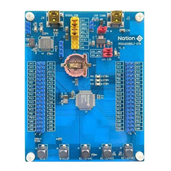
Page 4: Development Board Layout
The Mini USB interface (J3) is used to connect the DP and DM signals of the main MCU (U3) for the USB interface communication of the main MCU. 2 / 12 Nations Technologies Inc. Tel:+86-755-86309900 Email:info@nationstech.com Address: Nations Tower, #109 Baoshen Road, Hi-tech Park North. Nanshan District, Shenzhen, 518057, P.R.China... - Page 5 The GPIO interface of the chip is all led out, and the 3.3V voltage and GND pins are also reserved on the pins, which is convenient for testing. For the specific definition of the interface, please refer to 3 / 12 Nations Technologies Inc. Tel:+86-755-86309900 Email:info@nationstech.com Address: Nations Tower, #109 Baoshen Road, Hi-tech Park North. Nanshan District, Shenzhen, 518057, P.R.China...
-
Page 6: Development Board Jumper Instructions
"UM_N32A455 Series User Manual ". 1.4 Development Board Jumper Instructions Figure 1-2 Development Board Jumper Description 4 / 12 Nations Technologies Inc. Tel:+86-755-86309900 Email:info@nationstech.com Address: Nations Tower, #109 Baoshen Road, Hi-tech Park North. Nanshan District, Shenzhen, 518057, P.R.China... -
Page 7: Development Board Schematic
PA0 (set the PA0 bit as the WKUP signal). 1.5 Development board schematic The schematic diagram of the N32A455CEL7-STB development board is described as follows (For details, please refer to"N32A455CEL7-STB_V1.0"). 1) MCU connection Refer to Figure 1-3 for the schematic diagram of the MCU connection. Each VDD pin of the MCU is connected with a capacitor, and all GPIOs are connected to the J1 and J2 pins for easy debugging. - Page 8 Refer to Figure 1-5 for the schematic diagram of the key design. There are a total of 5 keys, which are the three general keys, the MCU wake-up key and reset key. 6 / 12 Nations Technologies Inc. Tel:+86-755-86309900 Email:info@nationstech.com Address: Nations Tower, #109 Baoshen Road, Hi-tech Park North. Nanshan District, Shenzhen, 518057, P.R.China...
- Page 9 D6 and D7 are used for NS-LINK MCU control to monitor the running status of NS-LINK. Figure 1-6 LED Light Design 7 / 12 Nations Technologies Inc. Tel:+86-755-86309900 Email:info@nationstech.com Address: Nations Tower, #109 Baoshen Road, Hi-tech Park North. Nanshan District, Shenzhen, 518057, P.R.China...
- Page 10 Refer to Figure 1-8 for the external schematic diagram of the BAT battery, which can supply power to the VBAT pin through the external battery holder on the PCB board and an external CR1220 battery 8 / 12 Nations Technologies Inc. Tel:+86-755-86309900 Email:info@nationstech.com Address: Nations Tower, #109 Baoshen Road, Hi-tech Park North. Nanshan District, Shenzhen, 518057, P.R.China...
- Page 11 DEBUG USB port, omitting the ULINK or JLINK writer. You can also debug through DEBUG analog serial port. Figure 1-9 NS-LINK 9 / 12 Nations Technologies Inc. Tel:+86-755-86309900 Email:info@nationstech.com Address: Nations Tower, #109 Baoshen Road, Hi-tech Park North. Nanshan District, Shenzhen, 518057, P.R.China...
- Page 12 32.768KHz crystal needs to be connected close to the pin, and it can be omitted if there is no need. DP, DM: 33Ω series resistance, placed close to the pins 10 / 12 Nations Technologies Inc. Tel:+86-755-86309900 Email:info@nationstech.com Address: Nations Tower, #109 Baoshen Road, Hi-tech Park North. Nanshan District, Shenzhen, 518057, P.R.China...
-
Page 13: Version History
2 Version history Version Date Modify V1.0 2023-02-25 Initial version 11 / 12 Nations Technologies Inc. Tel:+86-755-86309900 Email:info@nationstech.com Address: Nations Tower, #109 Baoshen Road, Hi-tech Park North. Nanshan District, Shenzhen, 518057, P.R.China... -
Page 14: Notice
This document is the exclusive property of Nations Technologies Inc. (Hereinafter referred to as NATIONS). This document, and the product of NATIONS described herein (Hereinafter referred to as the Product) are owned by NATIONS under the laws and treaties of the People’s Republic of China and other applicable jurisdictions worldwide.
Need help?
Do you have a question about the N32A455CEL7-STB and is the answer not in the manual?
Questions and answers