Table of Contents
Advertisement
Quick Links
BQ76972 3-Series to 16-Series High Accuracy Battery Monitor and Protector for
1 Features
•
Battery monitoring capability for 3-series to 16-
series cells
•
High accuracy cell voltage measurement of ±3.0
mV
•
Integrated charge pump for high-side NFET
protection with optional autonomous recovery
•
Extensive protection suite including voltage,
temperature, current, and internal diagnostics
•
Two independent ADCs
– Support for simultaneous current and voltage
sampling
– High-accuracy coulomb counter with input
offset error < 1 µV (typical)
•
Wide-range current applications (±200-mV
measurement range across sense resistor)
•
Integrated secondary chemical fuse drive
protection
•
Autonomous or host-controlled cell balancing
•
Multiple power modes (typical battery pack
operating range conditions)
– NORMAL mode: 286 µA
– Multiple SLEEP mode options: 24 µA to 41 µA
– Multiple DEEPSLEEP mode options: 9 µA to 10
µA
– SHUTDOWN mode: 1 µA
•
High-voltage tolerance of 85 V on cell connect and
select additional pins
•
Tolerant of random cell attach sequence on
production line
•
Support for temperature sensing using internal
sensor and up to nine external thermistors
•
Integrated one-time-programmable (OTP) memory
programmable by customers on production line
•
Communication options include 400-kHz I
and HDQ one-wire interface
•
Dual-programmable LDOs for external system
usage
•
48-pin TQFP package (PFB)
An IMPORTANT NOTICE at the end of this data sheet addresses availability, warranty, changes, use in safety-critical applications,
intellectual property matters and other important disclaimers. PRODUCTION DATA.
Li-Ion, Li-Polymer, and LiFePO
2
C, SPI,
Battery Packs
4
2 Applications
•
Energy storage systems
•
Battery backup unit (BBU)
•
E-bike, e-scooter, and LEV
•
Cordless power tools and garden tools
•
Non-military drones
•
Other industrial battery pack (≥10series)
3 Description
The Texas Instruments BQ76972 device is a
highly integrated, high-accuracy battery monitor
and protector for 3-series to 16-series Li-ion, Li-
polymer, and LiFePO
4
includes a high-accuracy monitoring system, a
highly configurable protection subsystem, and support
for autonomous or host controlled cell balancing.
Integration includes high-side charge-pump NFET
drivers, dual programmable LDOs for external system
use, and a host communication peripheral supporting
2
400-kHz I
C, SPI, and HDQ one-wire standards.
The BQ76972 device is available in a 48-pin TQFP
package.
Device Information
(1)
PART NUMBER
PACKAGE
BQ76972xy
PFB (48-pin)
(1)
See the
Device Comparison Table
device family. For all available devices, see the orderable
addendum at the end of the data sheet.
+
VC15
+
VC14
+
VC13
+
VC12
+
VC11
+
+
VC10
VC9
+
+
VC8
+
VC7
VC6
+
+
VC5
VC4
+
+
+
+
Simplified Schematic
BQ76972
SLUSFC9 – DECEMBER 2023
battery packs. The device
BODY SIZE (NOM)
7 mm × 7 mm
for information on the
PACK+
CHG
DSG
COMM TO
SYSTEM
COMMUNICATIONS
5 V
TRANSCEIVER
COMM
REGIN
REG1
VDD
REG2
3.3 V
RST_SHUT
DDSG
MCU
DCHG
DFETOFF
CFETOFF
HDQ
SDA
SCL
ALERT
GND
PACK–
Advertisement
Table of Contents

Related Manuals for Texas Instruments BQ76972


Summary of Contents for Texas Instruments BQ76972
-
Page 1: Features
BQ76972 SLUSFC9 – DECEMBER 2023 BQ76972 3-Series to 16-Series High Accuracy Battery Monitor and Protector for Li-Ion, Li-Polymer, and LiFePO Battery Packs 1 Features 2 Applications • Battery monitoring capability for 3-series to 16- • Energy storage systems series cells •... -
Page 2: Table Of Contents
Caution........80 6.26 High-side NFET Drivers.......... Glossary..............80 6.27 Comparator-Based Protection Subsystem....20 10 Revision History............6.28 Timing Requirements - I C Interface, 100kHz 11 Mechanical, Packaging, Orderable Information..80 Mode................Submit Document Feedback Copyright © 2023 Texas Instruments Incorporated Product Folder Links: BQ76972... -
Page 3: Device Comparison Table
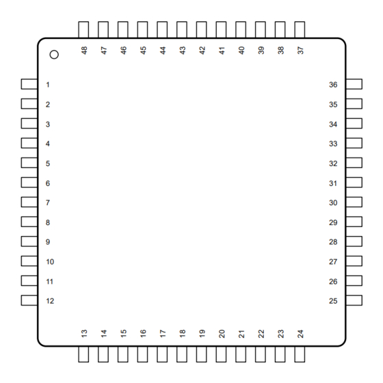
VC10 DCHG DFETOFF CFETOFF ALERT Not to scale Table 5-1. BQ76972 TQFP Package (PFB) Pin Functions TYPE DESCRIPTION NAME Sense voltage input pin for the fifteenth cell from the bottom of the stack, balance current VC15 input for the fifteenth cell from the bottom of the stack, and return balance current for the... - Page 4 BQ76972 www.ti.com SLUSFC9 – DECEMBER 2023 Table 5-1. BQ76972 TQFP Package (PFB) Pin Functions (continued) TYPE DESCRIPTION NAME Sense voltage input pin for the eleventh cell from the bottom of the stack, balance VC11 current input for the eleventh cell from the bottom of the stack, and return balance...
- Page 5 BQ76972 www.ti.com SLUSFC9 – DECEMBER 2023 Table 5-1. BQ76972 TQFP Package (PFB) Pin Functions (continued) TYPE DESCRIPTION NAME Multifunction pin, can be CFETOFF, SPI_CS, thermistor input, general purpose ADC CFETOFF I/OD, I/OA input, or general purpose digital output Multifunction pin, can be DFETOFF, BOTHOFF, thermistor input, general purpose ADC...
-
Page 6: Specifications
Input voltage range, V VC10 VSS–0.3 and VSS+85 VC9–0.3 maximum of Input voltage range, V VSS–0.3 and VSS+85 VC8–0.3 maximum of Input voltage range, V VSS–0.3 and VSS+85 VC7–0.3 Submit Document Feedback Copyright © 2023 Texas Instruments Incorporated Product Folder Links: BQ76972... -
Page 7: Esd Ratings
Charged device model (CDM), per ANSI/ESDA/ Electrostatic discharge ±250 (ESD) JEDEC JS-002, all pins JEDEC document JEP155 states that 500-V HBM allows safe manufacturing with a standard ESD control process. Copyright © 2023 Texas Instruments Incorporated Submit Document Feedback Product Folder Links: BQ76972... -
Page 8: Recommended Operating Conditions
VSS + 2.0 VSS + 80 External cell input resistance Ω External cell input 0.22 µF (2) (5) capacitance Output voltage range Output voltage range CHG, DSG, CP1 Submit Document Feedback Copyright © 2023 Texas Instruments Incorporated Product Folder Links: BQ76972... -
Page 9: Thermal Information Bq76952
10.7 µA DEEPSLEEP_1 communication No monitoring or protections, REG1 = 3.3 V DEEPSLEEP Mode with no load, REG2 = OFF, LFO = OFF, no µA DEEPSLEEP_2 communication Copyright © 2023 Texas Instruments Incorporated Submit Document Feedback Product Folder Links: BQ76972... -
Page 10: Digital I/O
V to 80 V (unless otherwise noted) PARAMETER TEST CONDITIONS UNIT Internal pullup current from BAT pin to LD ≥ 4.7 V, V = VSS µA (PULLUP) pin, used for load detect functionality Submit Document Feedback Copyright © 2023 Texas Instruments Incorporated Product Folder Links: BQ76972... -
Page 11: Precharge (Pchg) And Predischarge (Pdsg) Fet Drive
External capacitor, REG18 to VSS µF REG18 Regulator voltage REG18 ΔV vs (V at 25°C), I REG18 REG18 REG18 ΔV Regulator output over temperature ±0.15% O(TEMP) mA, V = 55 V Copyright © 2023 Texas Instruments Incorporated Submit Document Feedback Product Folder Links: BQ76972... -
Page 12: Reg0 Pre-Regulator
25°C, I REG1 REG1 REG1 ΔV Regulator output over temperature 20 mA, V = 5.5 V, V set to ±0.25% O(TEMP) REGIN REG1 nominal 3.3 V setting) Submit Document Feedback Copyright © 2023 Texas Instruments Incorporated Product Folder Links: BQ76972... -
Page 13: Reg2 Ldo
PPM/°C (REF1DRIFT) VOLTAGE REFERENCE 2 Internal reference voltage = 25°C 1.23 1.24 1.25 (REF2) (3) (4) Internal reference voltage drift = –10°C to 60°C ±20 PPM/°C (REF2DRIFT) Copyright © 2023 Texas Instruments Incorporated Submit Document Feedback Product Folder Links: BQ76972... -
Page 14: Coulomb Counter
Code stability is defined as the resolution such that the data exhibits 3-sigma variation within ±1-LSB. Specified by a combination of design and production test Submit Document Feedback Copyright © 2023 Texas Instruments Incorporated Product Folder Links: BQ76972... -
Page 15: Current Measurement Digital Filter (Cc2)
Input voltage range applicable to external thermistor (external thermistor measurements using the TS1, TS2, TS3, –0.2 (ADC_IN_TS) REG18 measurement mode) ALERT, CFETOFF, DFETOFF, HDQ, DCHG, and DDSG pins Copyright © 2023 Texas Instruments Incorporated Submit Document Feedback Product Folder Links: BQ76972... - Page 16 Config[FASTADC] = 1 Stack voltage (VC16 – 0 V < V < 80 V, T = –40°C to VC16 –0.5 STACK(ACC) VSS) measurement 85°C accuracy Submit Document Feedback Copyright © 2023 Texas Instruments Incorporated Product Folder Links: BQ76972...
-
Page 17: Cell Voltage Measurement Accuracy
Specified by a combination of characterization and production test, using 16-series stack, input network series resistance = 20-Ω, differential capacitance = 220-nF, cell balancing inactive Copyright © 2023 Texas Instruments Incorporated Submit Document Feedback Product Folder Links:... -
Page 18: Cell Balancing
5.5 V or 11 V mode), the maximum voltage on V should be reduced to ensure the voltage on CP1, CHG, and DSG does not exceed their maximum specified voltage. Submit Document Feedback Copyright © 2023 Texas Instruments Incorporated Product Folder Links: BQ76972... -
Page 19: Internal Oscillators
DSG pin voltage with CHG/DSG C = 20 nF, charge pump high (FETON_HI_LOBAT) respect to BAT, 4.7 V overdrive setting ≤ V < 8 V, V ≤ Copyright © 2023 Texas Instruments Incorporated Submit Document Feedback Product Folder Links: BQ76972... -
Page 20: Comparator-Based Protection Subsystem
V to 80 V (unless otherwise noted) PARAMETER TEST CONDITIONS UNIT 1.012 V to 5.566 Overvoltage detection range Nominal setting (50.6 mV steps) (OVP) V in 50.6 mV steps Submit Document Feedback Copyright © 2023 Texas Instruments Incorporated Product Folder Links: BQ76972... - Page 21 –80, –100, –125, Short circuit in discharge voltage Nominal settings, threshold based on –150, (SCD) threshold range – V –175, –200, –250, –300, –350, –400, –450, –500 Copyright © 2023 Texas Instruments Incorporated Submit Document Feedback Product Folder Links: BQ76972...
-
Page 22: Timing Requirements - I
SU:DAT Clock rise time 10% to 90% 1000 Clock fall time 90% to 10% Setup time STOP condition µs SU:STO Bus free time STOP to START µs Submit Document Feedback Copyright © 2023 Texas Instruments Incorporated Product Folder Links: BQ76972... -
Page 23: Timing Requirements - I
CYCD Device Write 1 Time Device drives HDQ µs Device Write 0 Time Device drives HDQ µs (2) (4) Device Response Time Device drives HDQ µs RSPS Copyright © 2023 Texas Instruments Incorporated Submit Document Feedback Product Folder Links: BQ76972... -
Page 24: Timing Requirements - Spi Interface
This assumes 15 ns setup time on the SPI controller for MISO. If additional setup time is required, the clock period should be extended accordingly. When SPI pin filtering is enabled, pulses on input pins of duration below 200 ns may be filtered out. Submit Document Feedback Copyright © 2023 Texas Instruments Incorporated Product Folder Links: BQ76972... -
Page 25: Interface Timing Diagrams
L S B O U T SPI_MISO t SU t HI SPI_MOSI « %,7 M S B IN L S B IN Figure 6-2. SPI Communications Interface Timing Copyright © 2023 Texas Instruments Incorporated Submit Document Feedback Product Folder Links: BQ76972... - Page 26 HDQ Host to Device communication d. Device to HDQ Host communication e. Device to HDQ Host response format f. HDQ Host to Device Figure 6-3. HDQ Communications Interface Timing Submit Document Feedback Copyright © 2023 Texas Instruments Incorporated Product Folder Links: BQ76972...
-
Page 27: Typical Characteristics
Figure 6-6. Internal Temperature Sensor (Delta V LFO measured in FULL SPEED mode (262 kHz) Voltage vs. Temperature Figure 6-7. Low Frequency Oscillator (LFO) Accuracy vs. Temperature Copyright © 2023 Texas Instruments Incorporated Submit Document Feedback Product Folder Links: BQ76972... - Page 28 Figure 6-11. Cell Balancing Resistance vs. (OCC) Threshold vs. Temperature Temperature Figure 6-12. Cell Balancing Resistance vs. Cell Figure 6-13. REG1 Voltage vs. Load at 25°C Common-Mode Voltage at 25°C Submit Document Feedback Copyright © 2023 Texas Instruments Incorporated Product Folder Links: BQ76972...
- Page 29 Figure 6-17. Coulomb Counter Gain Error vs. Temperature Figure 6-18. LD Wake Voltage vs. Temperature Figure 6-19. REG18 Voltage vs. Temperature, with No Load Copyright © 2023 Texas Instruments Incorporated Submit Document Feedback Product Folder Links: BQ76972...
- Page 30 Figure 6-23. BAT Current in SHUTDOWN Mode vs. Temperature Temperature Figure 6-24. BAT Current in SLEEP2 (SRC Figure 6-25. BAT Current in DEEPSLEEP2 (No Follower) Mode vs. Temperature LFO) Mode vs. Temperature Submit Document Feedback Copyright © 2023 Texas Instruments Incorporated Product Folder Links: BQ76972...
-
Page 31: Detailed Description
SLUSFC9 – DECEMBER 2023 7 Detailed Description 7.1 Overview The BQ76972 device is a highly integrated, accurate battery monitor and protector for 3-series to 16-series Li-ion, Li-polymer, and LiFePO battery packs. A high-accuracy voltage, current, and temperature measurement provides data for host-based algorithms and control. A feature-rich and highly configurable protection subsystem provides a wide set of protections that can be triggered and recovered completely autonomously by the device or under full control of a host processor. -
Page 32: Functional Block Diagram
Table. 7.4 Diagnostics The BQ76972 device includes a suite of diagnostic tests the system can use to improve operation robustness. These include comparisons between the two voltage references integrated within the device, a hardware monitor of the LFO frequency, memory checks at power-up or reset, an internal watchdog on the embedded processor, and more. -
Page 33: Measurement Subsystem
Manual. 7.5.2 Configuration Using OTP or Registers The BQ76972 device includes registers, with values that are stored in the RAM and can be loaded automatically from one-time programmable (OTP) memory. At initial power-up, the device loads OTP settings into registers, which are used by the device firmware during operation. - Page 34 7.6.1.2 Usage of VC Pins for Cells Versus Interconnect If the BQ76972 device is used in a system with fewer than 16-series cells, the additional cell inputs can be utilized to improve measurement performance. For example, a long connection may exist between two cells in...
- Page 35 7.6.1.3 Cell 1 Voltage Validation During SLEEP Mode In rare cases, an invalid Cell 1 Voltage() reading has been observed to occur in some devices taken during SLEEP mode. Copyright © 2023 Texas Instruments Incorporated Submit Document Feedback Product Folder Links:...
- Page 36 ADC is effectively 1.6667 × VREF1, which is approximately 2.02 V during normal operation. The BQ76972 device also reports the raw ADC counts when a measurement is taken using the TS1 pin. This data can be used during manufacturing to better calibrate the ADCIN functionality.
- Page 37 7.6.5 Internal Temperature Measurement The BQ76972 device integrates the capability to measure its internal die temperature by digitizing the difference in internal transistor base-emitter voltages (delta-V ). This voltage is measured periodically as part of the measurement loop and is processed to provide a reported temperature value available through the digital communications interface.
- Page 38 7.6.7 Factory Trim of Voltage ADC The BQ76972 device includes factory trim for the cell voltage ADC measurements in order to optimize the voltage measurement performance even if no further calibration is performed by the customer. Calibration can be performed by the customer on the production line to further optimize the performance in the system.
- Page 39 –0.2 –0.4 (mV) During operation, the cell measurements are read from the BQ76972 as Cell 1 Voltage(), Cell 2 Voltage(), and so on. The host then calculates adjusted values for each cell voltage: • Final Cell 1 Voltage = Cell 1 Voltage() – Cell 1 Offset •...
- Page 40 Figure 7-5. The BQ76972 is powered, and measurements of each cell voltage are read and stored (Cell 1 Voltage(), Cell 2 Voltage(), and so on). Multiple readings for each cell voltage can be collected and averaged to reduce the effect of noise that may be present on the production line.
- Page 41 Alternatively, the customer can collect offset data on a number of devices and analyze the resulting offsets, to determine whether using a fixed set of offsets may still provide sufficient cell measurement accuracy. This would Copyright © 2023 Texas Instruments Incorporated Submit Document Feedback...
- Page 42 ADCIN measurement gain in Calibration:Voltage:ADC Gain. If values for the calibration gain configuration are not written, the BQ76972 device will use factory trim or default values for the respective gain values. When a calibration gain configuration value is written, the device will use that in place of any factory trim or default gain.
- Page 43 VC16 and VC15 that is equal to the desired COV threshold. Next, the CAL_COV() subcommand is sent by the host, which causes the BQ76972 device to perform a search for the appropriate calibration coefficients to realize a COV threshold at or close to the applied voltage level.
-
Page 44: Primary And Secondary Protection Subsystems
When a Permanent Fail has occurred, the BQ76972 device can be configured to either simply provide a flag, or to indefinitely disable the protection FETs, or to assert the FUSE pin to permanently disable the pack. The FUSE pin can be used to blow an in-line fuse and also can monitor if a separate secondary protector IC has attempted to blow the fuse. - Page 45 Host Watchdog Fault Protection 7.7.3 Secondary Protections The BQ76972 device integrates a suite of secondary protection checks on battery operation and status that can trigger a Permanent Fail (PF) if conditions are considered so serious that the pack should be permanently disabled.
- Page 46 Top of Stack Versus Cell Sum Permanent Fail 7.7.4 High-Side NFET Drivers The BQ76972 device includes an integrated charge pump and high-side NFET drivers for driving CHG and DSG protection FETs. The charge pump uses an external capacitor connected between the BAT and CP1 pins that is charged to an overdrive voltage when the charge pump is enabled.
- Page 47 FETs. When a series FET configuration is used, the BQ76972 device provides body diode protection for the case when one FET is off and one FET is on.
-
Page 48: Device Hardware Features
VC16, PACK, and LD pins. 7.8.3 LDOs The BQ76972 device contains an integrated 1.8-V LDO (REG18) that provides a regulated 1.8 V supply voltage for the device's internal circuitry and digital logic. This regulator uses an external capacitor connected to the REG18 pin, and it should only be used for internal circuitry. - Page 49 7.8.3.2 REG1 and REG2 LDO Controls The REG1 and REG2 LDOs in the BQ76972 device are for customer use, and their output voltages can be programmed independently to 1.8 V, 2.5 V, 3.0 V, 3.3 V, or 5.0 V. The REG1 and REG2 LDOs and the REG0 preregulator are disabled by default in the BQ76972 device.
- Page 50 Pin can be used for general purpose ADC measurement 7.8.6 RST_SHUT Pin Operation The RST_SHUT pin provides a simple way to reset or shutdown the BQ76972 device without needing to use serial bus communication. During normal operation, the RST_SHUT pin should be driven low. When the pin is driven high, the device will immediately reset most of the digital logic, including that associated with the serial communications bus.
- Page 51 7.8.10 Fuse Drive The FUSE pin on the BQ76972 device can be used to blow a chemical fuse in the presence of a Permanent Fail (PF), as well as to determine if an external secondary protector in the system has detected a fault and is attempting to blow the fuse itself.
- Page 52 7.8.11 Cell Open Wire The BQ76972 device supports the detection of a broken connection between a cell in the pack and the cell attachment to the PCB containing BQ76972. Without this check, the voltage at the cell input pin of the BQ76972 device may persist for some time on the board-level capacitor, leading to incorrect voltage readings.
-
Page 53: Device Functional Modes
SLUSFC9 – DECEMBER 2023 7.8.13 High Frequency Oscillator The high frequency oscillator (HFO) in the BQ76972 device operates at 16.78 MHz and is frequency locked to the LFO. The HFO powers up as needed for internal logic functions. 7.9 Device Functional Modes 7.9.1 Overview... - Page 54 SLEEP mode. The BQ76972 device will exit SLEEP mode if a protection fault occurs, or current begins flowing, or a charger is attached, or if forced by subcommand, or if the RST_SHUT pin is asserted for < 1 s. When exiting based on...
- Page 55 While the BQ76972 device is in NORMAL mode or SLEEP mode, the device can also be configured to enter SHUTDOWN mode if the internal temperature measurement exceeds a programmed temperature threshold for a programmed delay.
-
Page 56: Serial Communications Interface
C serial communications interface in the BQ76972 device acts as a responder device and supports rates up to 400 kHz with an optional CRC check. If the OTP is not programmed, the BQ76972 device will initially power up by default in 400 kHz I... - Page 57 + x + 1, and the initial value is 0. When the controller detects an invalid CRC, the I C controller will NACK the CRC, which causes the I responder to go to an idle state. Copyright © 2023 Texas Instruments Incorporated Submit Document Feedback Product Folder Links: BQ76972...
- Page 58 7.10.3 SPI Communications The SPI interface in the BQ76972 device operates as a responder-only interface with an optional CRC check. If the OTP has not been programmed, the BQ76972 device initially powers up by default in 400 kHz I C mode,...
- Page 59 CRC error was detected. The internal oscillator in the BQ76972 device may not be running when the host initiates a transaction (for example, this can occur if the device is in SLEEP mode). If this occurs, the interface will drive out 0xFFFF on SPI_MISO for the first 16-bits clocked out.
- Page 60 SPI_MISO 8-bit CRC Previous R/W bit Previous 8-bit & 7-bit address write or read data (for previous two bytes) Figure 7-12. SPI Transaction #1 Using CRC Submit Document Feedback Copyright © 2023 Texas Instruments Incorporated Product Folder Links: BQ76972...
- Page 61 R/W bit & 7-bit 8-bit write or 8-bit CRC address # 2 read data # 2 (for previous two bytes) Figure 7-14. SPI Transaction #3 Using CRC Copyright © 2023 Texas Instruments Incorporated Submit Document Feedback Product Folder Links: BQ76972...
- Page 62 # 2 (or don’t care if read) SPI_MISO R/W bit & 7-bit 8-bit write address # 1 data # 1 Figure 7-16. SPI Transaction #2 Without CRC Submit Document Feedback Copyright © 2023 Texas Instruments Incorporated Product Folder Links: BQ76972...
- Page 63 The HDQ interface is an asynchronous return-to-one protocol where a processor communicates with the BQ76972 device using a single-wire connection to the ALERT pin or the HDQ pin, depending on the configuration. The controller (host device) and the responder (the BQ76972 device) drive the HDQ interface using an open-drain driver with a pullup resistor from the HDQ interface to a supply voltage required on the circuit board.
-
Page 64: Cell Balancing
BQ76972 Technical Reference Manual. Due to the current that flows into the cell input pins on the BQ76972 device while balancing is active, the measurement of cell voltages and evaluation of cell voltage protections by the device is modified during balancing. -
Page 65: Application And Implementation
To help alleviate this, additional configuration bits are provided which cause the device to slow the measurement loop speed when cell balancing is active. The BQ76972 device will insert current-only measurements after each voltage and a temperature scan loop to slow down voltage measurements and thereby increase the average balancing current. - Page 66 400 nF, then changing CP1 to a value of 2200 nF will result in the 11-V charge pump level dropping to approximately 9 V, before being restored to the 11-V level by the charge pump. Submit Document Feedback Copyright © 2023 Texas Instruments Incorporated Product Folder Links: BQ76972...
- Page 67 ALERT PACK– Figure 8-1. BQ76972 16-Series Cell Typical Implementation (Simplified Schematic) A full schematic of a basic monitor circuit based on the BQ76972 for a 16-series battery pack is shown below. Section 8.8.2 shows the board layout for this design.
- Page 68 PGND TP19 0.1uF PGND 5.1k 7.50k TP20 5.1k PACK TP21 TP22 PGND TP23 100V PACK 5.1k 5.1k 5.1k 5.1k Figure 8-3. BQ76972 16-Series Cell Schematic Diagram—Additional Circuitry Submit Document Feedback Copyright © 2023 Texas Instruments Incorporated Product Folder Links: BQ76972...
- Page 69 BQ76972 www.ti.com SLUSFC9 – DECEMBER 2023 8.2.1 Design Requirements (Example) Table 8-1. BQ76972 Design Requirements DESIGN PARAMETER EXAMPLE VALUE Minimum system operating voltage 40 V Cell minimum operating voltage 2.5 V Series cell count Sense resistor 1 mΩ Number of thermistors...
- Page 70 FETs and their voltage handling requirements. If the FETs are selected with a maximum gate-to-source voltage of 15 V, then the 11 V overdrive mode within the BQ76972 device can be used. If the FETs are not specified to withstand this level, or there is a concern over gate leakage current on the FETs, the lower overdrive level of 5.5 V can be selected.
-
Page 71: Calibration Process
8.3 Random Cell Connection Support The BQ76972 device supports a random connection sequence of cells to the device during pack manufacturing. For example, cell-10 in a 16-cell stack might be first connected at the input terminals leading to pins VC10 and VC9, then cell-4 may next be connected at the input terminals leading to pins VC4 and VC3, and so on. -
Page 72: Startup Timing
8.4 Startup Timing At initial power up of the BQ76972 device from a SHUTDOWN state, the device progresses through a sequence of events before entering NORMAL mode operation. These are described below for an example configuration, with approximate timing shown for the cases when [FASTADC] = 0 and [FASTADC] = 1. -
Page 73: Fet Driver Turn-Off
DSG pin and the FET gate, and a light load on PACK+, such that the voltage on PACK+ drops slowly as the FET is disabled. The pulsing on the DSG pin can be seen lasting for approximately 170 μs. Copyright © 2023 Texas Instruments Incorporated Submit Document Feedback Product Folder Links:... - Page 74 Figure 8-7. Zoomed-In View of the Pulsing on the DSG Pin During FET Turn-Off A slower turn-off case is shown in Figure 8-8, using a 4.7-kΩ series gate resistor, and the PACK+ connector shorted to the top of stack. Submit Document Feedback Copyright © 2023 Texas Instruments Incorporated Product Folder Links: BQ76972...
-
Page 75: Unused Pins
8.6 Unused Pins Some device pins may not be needed in a particular application. The manner in which each should be terminated in this case is described below. Copyright © 2023 Texas Instruments Incorporated Submit Document Feedback Product Folder Links:... -
Page 76: Power Supply Requirements
8.7 Power Supply Requirements The BQ76972 device draws its supply current from the BAT pin, which is typically connected to the top of stack point through a series diode, to protect against any fault within the device resulting in unintended charging of the pack. - Page 77 BQ76972 www.ti.com SLUSFC9 – DECEMBER 2023 circuit ranges of the BQ76972 device. Parallel resistors can be used as long as good Kelvin sensing is ensured. The device is designed to support a 1-mΩ sense resistor. • In reference to the system circuitry, the following features require attention for component placement and layout: Differential Low-Pass Filter, and I C communication.
- Page 78 BQ76972 www.ti.com SLUSFC9 – DECEMBER 2023 Figure 8-10. BQ76952 Two-Layer Board Layout–Top Layer Submit Document Feedback Copyright © 2023 Texas Instruments Incorporated Product Folder Links: BQ76972...
- Page 79 BQ76972 www.ti.com SLUSFC9 – DECEMBER 2023 Figure 8-11. BQ76952 Two-Layer Board Layout–Bottom Layer Copyright © 2023 Texas Instruments Incorporated Submit Document Feedback Product Folder Links: BQ76972...
-
Page 80: Device And Documentation Support
All trademarks are the property of their respective owners. 9.4 Electrostatic Discharge Caution This integrated circuit can be damaged by ESD. Texas Instruments recommends that all integrated circuits be handled with appropriate precautions. Failure to observe proper handling and installation procedures can cause damage. - Page 81 RoHS & Green NIPDAU Level-2-260C-1 YEAR -40 to 85 BQ76972 Samples The marketing status values are defined as follows: ACTIVE: Product device recommended for new designs. LIFEBUY: TI has announced that the device will be discontinued, and a lifetime-buy period is in effect.
- Page 82 PACKAGE OPTION ADDENDUM www.ti.com 10-Dec-2023 In no event shall TI's liability arising out of such information exceed the total purchase price of the TI part(s) at issue in this document sold by TI to Customer on an annual basis. Addendum-Page 2...
- Page 83 PACKAGE MATERIALS INFORMATION www.ti.com 11-Dec-2023 TAPE AND REEL INFORMATION REEL DIMENSIONS TAPE DIMENSIONS B0 W Reel Diameter Cavity Dimension designed to accommodate the component width Dimension designed to accommodate the component length Dimension designed to accommodate the component thickness Overall width of the carrier tape Pitch between successive cavity centers Reel Width (W1) QUADRANT ASSIGNMENTS FOR PIN 1 ORIENTATION IN TAPE...
- Page 84 PACKAGE MATERIALS INFORMATION www.ti.com 11-Dec-2023 TAPE AND REEL BOX DIMENSIONS Width (mm) *All dimensions are nominal Device Package Type Package Drawing Pins Length (mm) Width (mm) Height (mm) BQ7697202PFBR TQFP 1000 336.6 336.6 31.8 BQ7697204PFBR TQFP 1000 336.6 336.6 31.8 BQ76972PFBR TQFP 1000...
-
Page 85: Package Outline
PACKAGE OUTLINE PFB0048A TQFP - 1.2 mm max height SCALE 1.900 PLASTIC QUAD FLATPACK PLASTIC QUAD FLATPACK NOTE 3 PIN 1 ID NOTE 3 0.27 44X 0.5 0.17 0.08 C A B 4X 5.5 1.2 MAX SEATING PLANE SEE DETAIL A 0.08 (0.13) 0.25... - Page 86 EXAMPLE BOARD LAYOUT PFB0048A TQFP - 1.2 mm max height PLASTIC QUAD FLATPACK SYMM SEE DETAILS 48X (1.35) 48X (0.25) SYMM (8.5) 44X (0.5) (R0.05) TYP (8.5) LAND PATTERN EXAMPLE EXPOSED METAL SHOWN SCALE:8X 0.05 MAX 0.05 MIN ALL AROUND ALL AROUND SOLDER MASK METAL...
- Page 87 EXAMPLE STENCIL DESIGN PFB0048A TQFP - 1.2 mm max height PLASTIC QUAD FLATPACK SYMM 48X (1.35) 48X (0.25) SYMM (8.5) 44X (0.5) (R0.05) TYP (8.5) SOLDER PASTE EXAMPLE SCALE:8X 4215157/A 03/2024 NOTES: (continued) 6. Laser cutting apertures with trapezoidal walls and rounded corners may offer better paste release. IPC-7525 may have alternate design recommendations.
- Page 88 TI products. TI’s provision of these resources does not expand or otherwise alter TI’s applicable warranties or warranty disclaimers for TI products. TI objects to and rejects any additional or different terms you may have proposed. IMPORTANT NOTICE Mailing Address: Texas Instruments, Post Office Box 655303, Dallas, Texas 75265 Copyright © 2024, Texas Instruments Incorporated...
Need help?
Do you have a question about the BQ76972 and is the answer not in the manual?
Questions and answers