Table of Contents
Advertisement
Quick Links
TV10 0096_3G-SDI Neo Interface board
TV10 00
666
P/N – TV10 0096: 3G/HD-SDI Neo interface board for LVDS zoom cameras
P/N – TV50 0020: Mounting kit for TV10 0096 - 3G/HD-SDI Neo I/F boards
Includes: 30-way micro-coax camera cable, 2-way cable (power supply), 10-way cable (RS232/TTL/Analog output), 7-way cable (GPIOs), right
angle black anodized bracket, screws and spacers
P/N – TV50 0021: Cable kit for TV10 0096 - 3G/HD-SDI Neo I/F boards
Includes: 30-way micro-coax camera cable, 2-way cable (power supply), 10-way cable (RS232/TTL/Analog output)
Available connectors: VOPTEM02 (MCX connector), VOPTEM03 (SMB connector), VOPTEM04 (No connector)
TECHNICAL MANUAL
3G/HD-SDI Neo
Technical Manual
1/17
1/17
Advertisement
Table of Contents

Summary of Contents for i2S Twiga TV10 009
- Page 1 TV10 0096_3G-SDI Neo Interface board TV10 00 1/17 3G/HD-SDI Neo Technical Manual P/N – TV10 0096: 3G/HD-SDI Neo interface board for LVDS zoom cameras P/N – TV50 0020: Mounting kit for TV10 0096 - 3G/HD-SDI Neo I/F boards Includes: 30-way micro-coax camera cable, 2-way cable (power supply), 10-way cable (RS232/TTL/Analog output), 7-way cable (GPIOs), right angle black anodized bracket, screws and spacers P/N –...
-
Page 2: Table Of Contents
TV10 0096_3G-SDI Neo Interface board TV10 00 2/17 Table of content Table of content ................................2 Revision History ................................3 Key features ..................................4 General description ................................4 Benefits of this solution ..............................4 Block diagram ..................................5 Video acquisition ................................5 Communication ................................ -
Page 3: Revision History
TV10 0096_3G-SDI Neo Interface board TV10 00 3/17 Revision History Date Revision Description Modified by Note 07/02/23 Creation of the document 19/01/24 Document refactoring 12/06/24 Add REG_CAM_UART_BYPASS Change DIP switch video format TECHNICAL MANUAL 3/17... -
Page 4: Key Features
TV10 0096_3G-SDI Neo Interface board TV10 00 4/17 Key features • 3G-SDI SMPTE 424M, HD-SDI 292 M • Video resolution up to 1080p60 • Ultra-low transmission latency (< 1ms) • Communication UART – RS232/TTL using VISCA • Setup & Update via UART •... -
Page 5: Block Diagram
TV10 0096_3G-SDI Neo Interface board TV10 00 5/17 Block diagram Video acquisition The main component is the FPGA for video acquisition. The board acquire LVDS video from the camera block with no latency deserialization to provide uncompressed 3G- SDI video output via an SDI converter. Communication An UART / RS232 converter allows the user to select RS232 or UART TTL 3V3 communication. -
Page 6: Accessing To The Video
TV10 0096_3G-SDI Neo Interface board TV10 00 6/17 Accessing to the video Quick setup Full HD Installation steps: 1. Connect the KEL cable between the board J2 and the camera. 2. Connect the SDI cable to the output connector of the board J6 and to the SDI monitor. 3. -
Page 7: Lvds Video Input Supported Resolutions
TV10 0096_3G-SDI Neo Interface board TV10 00 7/17 • Full HD Progressive 1920x1080p: it can be at 25, 29.97 or 30 FPS, the camera must be in Single mode. It can also be at 50, 59.94 or 60 FPS, with these video formats only, the camera must be in Dual mode to be able to send more data. -
Page 8: System Configuration
TV10 0096_3G-SDI Neo Interface board TV10 00 8/17 System configuration Communication Communication with the camera can be done through J4 connector. For the connector pinout please see paragraph Connectors. Communication can be set to either RS232 mode (according to EIA RS-232 specification) or TTL mode (UART with 3.3V compatibility). - Page 9 TV10 0096_3G-SDI Neo Interface board TV10 00 9/17 The camera answer follows this structure: The time between the acknowledgement and the completion packet depends on the command. The answer for an inquiry is Z0 5Y followed by the information requested with FF as end byte. If an error occurs, here the answer structure: Example: Zoom In command with a speed of 7 is 0x81 01 04 07 27 FF and the expected answer is 0x90 41 FF followed by 0x90 51 FF.
-
Page 10: To The Internal Registers
TV10 0096_3G-SDI Neo Interface board TV10 00 10/17 To the internal registers The board parameters are accessible from the connector J4 with VISCA protocol at Address 0x82. Register name Address Saved Set command Comments Inquiry Command Inquiry Answer REG_FPGA_VERSION_H 0x01 Software version MSB 0x82 09 06 01 FF 0xA0 50 01 00 0y FF... -
Page 11: Control Camera Video Format
TV10 0096_3G-SDI Neo Interface board TV10 00 11/17 Control camera video format Three DIP switches are used to select the video format of the camera. The board checks, when the camera power is on, if the camera video format corresponds to the switches, otherwise it sends a VISCA command to change the format. It can be changed dynamically;... -
Page 12: Board Status
TV10 0096_3G-SDI Neo Interface board TV10 00 12/17 Board Status The board can be in 4 different states: • Initialization: the video format and the camera are not detected yet. • Ready: the board is ready to use, the video format has been detected and the camera is recognized. •... -
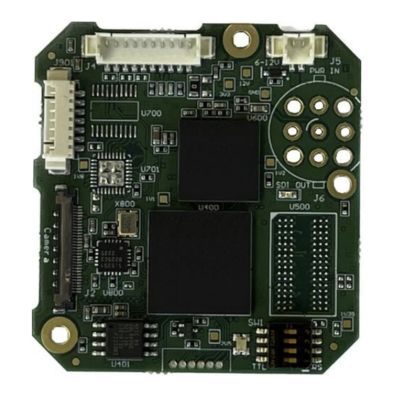
Page 13: Connectors
TV10 0096_3G-SDI Neo Interface board TV10 00 13/17 Connectors Communication External Power Supply 7 to 12 VDC UART-RX UART-TX BNC / MCX / SMB compatibility J901 GPIOs Zoom + Zoom - Focus Auto/Manual Focus Near Focus Far Freeze On/Off DIP switches Configuration LVDS input RS232... -
Page 14: Form Factor
TV10 0096_3G-SDI Neo Interface board TV10 00 14/17 Form factor BOTTOM 48mm (H) x 45mm (W) x 18mm (D) 4 holes Ø 3mm TECHNICAL MANUAL 14/17... -
Page 15: Troubleshooting
Update via UART An update of the board is possible by distance, you need an UART connection with the board and a Java application made by i2S. You can find the application and the different available software version on www.twiga-support.com where a changelog file gives you all the information about the features updated in each version. -
Page 16: Annex
TV10 0096_3G-SDI Neo Interface board TV10 00 16/17 Annex Annex 1: FPGA temperature table Here the table to get the FPGA temperature (°C) from the value read in the register 0x04. Register value read FPGA temperature (°C) 0x00 –58 0x01 –56 0x02 –54... -
Page 17: Annex 2: Video Format Table
TV10 0096_3G-SDI Neo Interface board TV10 00 17/17 0x2D 0x2E 0x2F 0x30 0x31 0x32 0x33 0x34 0x35 0x36 0x37 0x38 0x39 0x3A 0x3B 0x3C 0x3D 0x3E 0x3F Annex 2: Video format table Here the table to get the video format from the value read in the register 0x27. Register value read Video format 0x00...
Need help?
Do you have a question about the Twiga TV10 009 and is the answer not in the manual?
Questions and answers