
Summary of Contents for North Coast Synthesis MSK 015
- Page 1 MSK 015 Quad Voltage-Controlled Amplifier North Coast Synthesis Ltd. Matthew Skala April 23, 2023...
- Page 2 Documentation for the MSK 015 Copyright © 2023 Matthew Skala This documentation is free: you can redistribute it and/or modify it under the terms of the GNU General Public License as published by the Free Software Foundation, version 3. This documentation is distributed in the hope that it will be useful, but WITHOUT ANY WARRANTY;...
-
Page 3: Table Of Contents
Contents General notes Front panel controls and connections ........Inputs . - Page 4 Patch ideas Attenuator/mixer ..........Basic VCA .
-
Page 5: General Notes
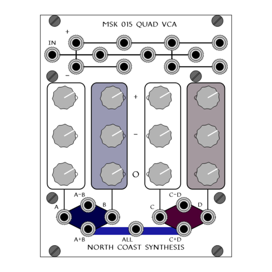
General notes This manual documents the MSK 014 Quad Voltage- channels if no other input cables are inserted. Controlled Amplifier, which is a module for use in There is similar normalling all the way across for a Eurorack modular synthesizer. This module con- the positive CVs, but the normalling for the nega- tains four identical channels. - Page 6 MSK 015 QUAD VCA NORTH COAST SYNTHESIS Figure 1: Module front panel.
-
Page 7: Module Function In Linear Mode
CV at 5V (the other at zero), will also give unity be difficult to achieve. The MSK 015 gives the user gain. a choice, but requires the user to make the choice, adjusting the knob while listening to the output for The offset knob and “bleed”... -
Page 8: Exponential Mode
VCA at all; and then MSK 015 when in exponential mode is limited by a stopping it at the VCA does not help much. For ex-... -
Page 9: Source Package
the mode-dependent limits on effective control voltage 2× 1.6mm PCBs described in earlier sections. 10mm 11mm Note the voltage limits apply to outputs as well stand- stand- front as inputs. For instance, if you set all channels to off off panel unity gain and apply +5V to all the signal inputs, then you will get +5V on all the per-channel out-... - Page 10 Sales dropped sharply in 2022, and unless I receive a lot more orders for modules and kits in 2023, this may be the last module design from North Coast Synthesis. Email should be sent to mskala@northcoastsynthesis.com.
-
Page 11: Safety And Other Warnings
Safety and other warnings Ask an adult to help you. Some lead-free solder alloys produce joints that North Coast Synthesis Ltd. does not offer war- look “cold” (i.e. defective) even when they are cor- ranties or technical support on anything we did not rectly made. -
Page 12: Bill Of Materials
Bill of materials This table is not a substitute for the text instructions. Value/Part No. ′′ C1, C2, C10–C12, 100pF radial ceramic, 0.2 lead spacing C14, C24–C26 ′′ C8, C22 4700pF film, 0.2 lead spacing C3–C7, C9, C15, 0.1µF axial ceramic C18–C21, C23, C27, ′′... - Page 13 Value/Part No. R9, R11, R12, 100kΩ vertical conductive plastic panel pot, BI Tech- R15–R17, R63, R65, nologies P0915N series, linear taper R66, R68–R70 R27, R28, R79, R80 100kΩ R31, R32, R83, R84 150kΩ R10, R20–R26, R59, 270kΩ R64, R72–R78 206–124 4-position SPDT DIP switch (CTS) U1–U4 TL074...
-
Page 14: Building Board 2
Except where noted, the order in which you add components does not matter much. Version 1 boards The first batch of MSK 015 boards had the value Install these capacitors where the symbol appears. for R54, R55, R102, and R103 indicated as 27kΩ on They are not polarized and may be installed in ei- the silkscreen;... - Page 15 This table is not a substitute for the text instructions. Value/Part No. ′′ C1, C10–C12, C14, 100pF radial ceramic, 0.2 lead spacing C24–C26 ′′ C8, C22 4700pF film, 0.2 lead spacing C3–C7, C9, C15, 0.1µF axial ceramic C18–C21, C23 ′′ C13, C16, C17 10µF radial aluminum electrolytic, 0.1...
-
Page 16: Fixed Resistors
100kΩ, which has a similar colour resistors R33, R34, R53, R85, and R86. Most of these code. An MSK 015 kit should also contain a ninth are used in the control voltage scaling networks (one 1kΩ resistor for use on Board 1. - Page 17 Install the four 3kΩ (orange-black-black-brown) in the control voltage scaling networks, specifically resistors R29, R30, R81, and R82. These are used to set the CV sensitivity in exponential mode. A full at the inputs of the control voltage scaling networks, kit should contain five 15kΩ...
- Page 18 Install the four 30kΩ (orange-black-black-red) re- Install the four 62kΩ (blue-red-black-red) resis- sistors R54, R55, R102, and R103. On version 1 tors R106–R109. These are used in the control volt- boards these footprints should be marked with stick- age scaling networks. ers.
-
Page 19: Diodes And Dip Sockets
The silkscreen markings on the board have code. A full MSK 015 kit should contain 17 270kΩ re- a corresponding stripe and the diodes should be in- sistors; the 13 resistors not used here are for Board 1. -
Page 20: Tl431 Voltage Reference
TL431 voltage reference The only component with a TO-92 package in the MSK 015 build is the TL431 voltage reference U8, which creates the +5V reference voltage for gain con- trol. It is polarized and must be installed in the cor- rect orientation to work;... -
Page 21: More Capacitors
Be careful not to install 100pF capacitors in the similar-looking footprints labelled “4700pF.” More capacitors Install the eight 100pF ceramic capacitors C1, C10– Install the two 4700pF film capacitors C8 and C12, C14, and C24–C26. These are compensation C22. These are special decoupling capacitors re- capacitors used to ensure stability on op amps that quired by the VCA chips’... -
Page 22: Trimmer Potentiometers
Install the three 10µF electrolytic capacitors C13, Install the five 10kΩ single-turn trimmers R47, C16, and C17, which filter the power supply for the R49, R50, R99, and R100. Four of these set the out- module as a whole and the +5V reference voltage. put gain (referenced to +5V control voltage in linear These are polarized components and they may ex- mode) for the four VCA channels. -
Page 23: Dip Switch
12V power. For most modules including the MSK 015, the red stripe should be at the bottom when the module is mounted vertically in a case. On the MSK 015, the correct location of the 12V supply is also marked with the text “... -
Page 24: Building Board 1 24 Preliminaries
Building Board 1 Board 1 has components on both sides, and for best Install these capacitors where the symbol appears. results, it is important to install them in the right They are not polarized and may be installed in either order. - Page 25 This table is not a substitute for the text instructions. Value/Part No. ′′ 100pF radial ceramic, 0.2 lead spacing C27, C28 0.1µF axial ceramic H1–H4 nut for M3 machine screw H9–H12 M3x11 M3 male-female standoff, 11mm body length H17–H20 M3x10 M3 male-female standoff, 10mm body length H21–H24 M3x6...
- Page 26 Install the 1kΩ (brown-black-black-brown) resis- Install the 15kΩ (brown-green-black-red) resistor tor R19. This is an output protection resistor for the R58. This is part of the voltage divider that sets the “master sum” output. Do not confuse it with the value of -VLO, the small negative reference voltage other power-of-ten value 100kΩ, which has a similar used by the offset knobs.
-
Page 27: Dip Socket
DIP socket Install the four 100kΩ (brown-black-black-orange) resistors R27, R28, R79, and R80. These set the Install the 8-pin DIP socket for the LF353 dual op- input impedance, and convert voltages to currents, erational amplifier U7. The amplifiers in this chip for the four channels of audio input. -
Page 28: Board To Board Connectors
nected to the output. It is unpolarized and may be Mate the three pairs of 10×1 header connectors installed in either direction. The capacitor will likely J22–J24 and P4–P6 and place them (do not sol- be marked “101” for the digits 1 and 0 followed by 1 der yet) in the J22–J24 footprints on Board 1 with more zero, thus 100, number of picofarads. -
Page 29: Panel Components
Solder J22–J24 and P4–P6 in place on the two Place (do not solder yet) the twelve panel poten- boards. Then remove Board 2 and the hex nuts hold- tiometers R9, R11, R12, R15 to R17, R63, R65, R66, ing it in place, but keep the standoffs attached to and R68 to R70 in their footprints. -
Page 30: Final Assembly
interfere with the proper functioning of the switching contacts. Final assembly Insert the LF353 chip U7 in its socket on Board 1. Be careful to insert it right way round: the end with Pin 1 will be marked by an indentation at one corner or a notch in the end and this end of the chip should be inserted to match the notch in the socket and on the board silkscreen and the rectangular Pin 1 solder... -
Page 32: Adjustment And Testing
Adjustment and testing This section describes how to adjust the five trimmers smoke, overheats, makes any unusual noises, or smells on the back of the Quad VCA for accurate unity gain bad. If any of those things happen, turn off the power at +5V control input and when the offset knobs are immediately, and troubleshoot the problem before turned to maximum. -
Page 33: Troubleshooting
Patch your reference signal into the signal input of more narrow a description you can find, the fewer channel A (leftmost channel) on the MSK 015. The places you will need to look to find what is wrong. normalling connections mean that this will actually The most common problems I see in my own apply the signal to all four channels. - Page 34 • its decoupling capacitors (the small ceramic ones) are installed and there is nothing wrong with their solder joints. You can try swapping a suspect chip with another one of the same type from elsewhere in the module and see if that causes the problem to change; if so, it’s likely that one of the two you swapped was bad.
-
Page 35: Patch Ideas
In all patches it’s best to experiment to see where two channels of the MSK 015 work with a dual what gives the most pleasing sound. oscillator, four envelope generators, two filters, an... -
Page 36: Fixed Voltage Gains
Nonetheless, it’s sometimes useful to multiply a volt- channel A input, it normals across to all four chan- age by a chosen small integer, and the MSK 015’s nels, and when they are set to unity gain the ALL trimmed unity gain makes that easy. -
Page 37: Mid-Side Encoding And Decoding
MSK 015 so that the signal will so you will need to either adjust for best sound or be well-balanced without careful adjustment. If you... -
Page 38: Voltage-Controlled Pan
four channels in a pattern other than the way the bipolar control voltages. However, then you may need normally connections work. Left channel for the first to experiment with the offset levels to get a pleasing stero signal to channel A, left of second signal to chan- effect, bearing in mind that the VCA channels can nel B, right channels of the two stereo signals to chan- only go a certain amount above unity gain. -
Page 39: Quadrature Madness
That is the difference of two multi- plications, and a function we can (almost) compute with the MSK 015. Why you would want to do so, is because of fre- quency shifting. Some frequency shifters (in partic-... - Page 40 Quad VCA’s A B and C D jacks, are combined with an external mixer – in this case a North Coast Synthesis MSK 011, though really any basic mixer would do. Using the ALL output on the Quad VCA would not work to do the mixing because it doesn’t invert...
-
Page 41: Circuit Explanation
Circuit explanation The MSK 015 Quad VCA is made up of a few simple itive input by half as much (0.05V) because of the kinds of sections, most of which are used multiple voltage divider driving the positive input. Then the times to build up the four-channel VCA. - Page 42 Figure 4: Control voltage input processing.
- Page 43 Figure 5: Add and subtract outputs.
-
Page 44: Vca Channels
Figure 6: Master sum output. pacitors bypassing the feedback networks to ensure 1980s-era Curtis CEM3360 dual VCA. It was selected stability, and series 1kΩ resistors to limit short-circuit for this module as an interesting chip with the de- current and also help with stability. The capacitors sired performance while being reasonably priced and kill the gain at higher-than-audio frequencies, so par- available in a through-hole package. - Page 45 The AS3360 data sheet does not spec- The MSK 015 module is intended to be able to ify an absolute maximum rating (i.e. an “exceed this produce above-unity voltage gain (unity at 5V lin- and you damage the chip”...
-
Page 46: Control Voltage Scaling
Figure 7: Main signal path for channel A. resistor. Bearing in mind that the input amplifier from about 0V to 1.7V, and an exponential voltage, had a gain of magnitude 1.5 and fed a 27kΩ resistor ranging from about 1.5V to 1.8V. The linear voltage to convert to current, to get the overall voltage gain is applied to the chip’s lograrithmic converter, gen- to 1.6 we need the feedback resistance of U2C to be... - Page 47 the cathode voltage approaches 0.6V the diode is 0.1–1.7V, which is a better fit. forward biased and starts to conduct, preventing the To achieve zero gain in linear mode the effective voltage from going any lower. The surrounding re- control voltage needs to go a little below zero, to bring sistors limit the current to safe levels in these cases.
-
Page 48: Notes On The Design Process
expo expo It made sense to limit the voltage with a Zener ⇒ diode to ground, which would give the right shape 15kΩ 62kΩ +5V 15kΩ to the allowed range (up to a certain amount from ground, down to not much below ground). I routinely 3.6kΩ... -
Page 49: Chip Gain Variation
in a circuit simulator with some of the combinations for adjusting the channel gain, and the idea is that that came out of Prolog. after building the module, these can be adjusted to When I thought I had a design that would work, compensate for the variation between chips. - Page 50 It would power up the chip under ufactured, individual manufacturing batches tend to conditions similar to the conditions in an MSK 015 at have narrower gain distribution but there’s a wider unity gain, and then produce an output voltage pro- variation from one batch to another, so my stock ac- portional to the chip’s gain (average across the two...
- Page 51 Figure 9: Power and reference voltage generation.
-
Page 52: Power And Reference Voltages
Power and reference voltages (which should be clean coming out of the regulator Figure shows the circuits which generate power and anyway) but helps guarantee stability. reference voltages for the module. The ±12V power The front panel offset pots also require a small rails are protected from reversal by series Schottky negative voltage, so that they can be adjusted to diodes, and there are 10µF electrolytic capacitors on... -
Page 53: Mechanical Drawings
Mechanical drawings On the following pages you will find: • the schematic diagram for the module; • a mock-up of what the completed module looks like from the front panel; • the top-side silk screen art showing component placement; • the bottom-side silk screen art showing compo- nent placement (note this drawing is mirrored, and shows what you actually see looking at the board, not the X-ray view used in other Kicad... - Page 55 MSK 015 QUAD VCA NORTH COAST SYNTHESIS...