Advertisement
Quick Links
BYTESAVER
INSTRUCTION MANUAL
B y t e s a v e r A s s e m b ly
• B y t e s a v e r P a r t s L i s t
B y t e m o v e r S o f t w a r e
• 2 7 0 8 - 2 7 0 4 P B O M D a t a
• B y t e m o v e r A s s e m b ly L i s t i n g
© Copyright 19 76. Alt rights reserved.
Cromemco
Specialists in computer peripherals
2432 Charleston Rd., Mountain Viaw, CA 94043 • (416) 964-7400
Advertisement

Related Manuals for Cromemco BYTESAVER


Summary of Contents for Cromemco BYTESAVER
- Page 1 BYTESAVER INSTRUCTION MANUAL B y t e s a v e r A s s e m b ly • B y t e s a v e r P a r t s L i s t B y t e m o v e r S o f t w a r e •...
- Page 3 (A 15, A 14 and A 13) may be tied to either the corresponding soldering iron. " H " or " L " terminal. For example, in order for the Bytesaver to reside in the top 8K of memory, the three jumpers should be in...
- Page 4 BY TESA VEH P A R T S L IS T B y t e s a v e r P a r t s L i s t Integrated Circuits Capacitors IC 1 .............. 74123 C1-C8............0.1 uF IC2 ..............7474 C9-C15..........
- Page 5 If the PROM to which you want to add software is PROM dress switches should be in the down position. zero on the Bytesaver board, turn o ff the A.C. power to the 6. Raise the examine switch. You are now examining the con...
- Page 6 PROM will be transfered to RAM. The contents of PROM are PROMs. Given that these seven PROMs are in PROM locations one through seven of the Bytesaver board, 8K BASIC can easily unaffected by this operation. 6. Raise the stop switch.
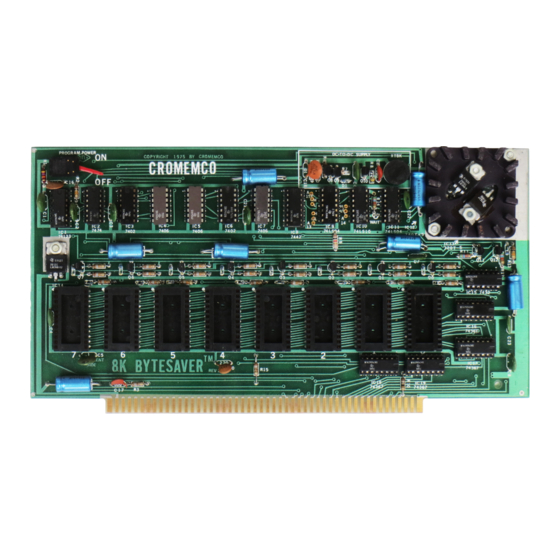
- Page 7 Protect position (PROM cannot be programmed). I Increasing memory address. PROM FIGURE 3: Bytesaver phsical layout. Erasing PROMS: The 2704 and 2708 PROMs are erased by View, CA 94040. A more expensive, but professional quality shining intense U .V . light through their quartz windows. One PROM eraser is available for $125 from Prometrics, 5345 North such U .V.
- Page 8 0 0 0 0 0 0 0 0 * BYTEMOVER <T. M. ) SOFTWARE FOR 0 0 0 0 0001 * CROMEMCO 8K BYTESAVER (T . M. ) 0 0 0 0 0 0 0 2 * VERSION 3. 1...
- Page 9 B Y T EM O V E R A SS E M B L Y L IS T IN G 0 0 3 4 E6 80 0350 ANI 128 0 0 3 6 OF 0 3 6 0 0 0 3 7 OF 0 3 7 0 0 0 3 8 C6 2D 0 3 8 0...
- Page 10 B Y T E M O V E R A SS E M B L Y L I S T I N G SJW BW W W Sf t l i f f l 006C 10 9 9 * TO MOVE DATA FROM ROM TO RAM 006C F I 1 1 0 0 POP 6...
- Page 11 B Y T E M O V E R A S S E M B L Y L IS T IN G 0 09 E 4 7 1 4 9 5 MOV B* A 0 0 9 F 1 4 9 9 * GO BACK TO 1 0 9 0 0 0 9 F E9 15 0 0 PCHL...
- Page 12 B Y T EM O V E R A SS E M B L Y L IS T IN G OODE 7A 2 6 5 0 MOV A, D OODF C6 0 4 2 6 6 0 AD I 4 OOEI 57 2 6 7 0 MOV D.
-
Page 13: Pin Names
2708-2704 P R O M D A T A PIN CON FIG U RA TIO N S BLOCK D IA G R A M DATA OUTPUT < V °, A s C D ' f e B A * C □... - Page 14 2708-2704 P R O M D A T A W a v e f o r m s (Logic levels and timing reference levels same as in the Read Mode unless noted otherwise.) Program Mode CS/WE = + 1 2 V Read/Program/Read Transitions...
- Page 15 2708-2704 P R OM D A T A S ■ » — A C C h a ra c te ris tic s = 0°C to 70°C, Vcc = +5V ±5%, VDD = +12V ±5%, V BB = -5 V ±5%, Vss = OV, Unless Otherwise Noted. Parameter Min.
-
Page 16: Programming & Operation
2708-2704 P R O M D A T A ACCESS TIME VS. TEMPERATURE -OAD + IOC VF 1 TTL P R O G R A M M IN G O P E R A T I O N D e s c r ip tio n Initially, and after each erasure, all bits of the 2708/2704 are in the "... -
Page 17: Ordering Information
PROM. PROMs used in Bytesaver may be erased with ultraviolet light, so that they may be used again and again. The Bytesaver may be used with 2304 or 2308 ROMs or with 2704 or 2708 PROMs. - Page 19 (ty io m e m c fr ™ COPYRIGHT 1975 BY CROMEMCO BOARD REV. 2 SCHEMATIC REV. 2 NOTE: 1. DASHED MODIFICATION FOR ROM RESIDENT INTERRUPT OPERATION (NOT INCLUDED ON STANDARD CARD) 2. ALL DIODES ARE IDENTICAL {IN9I4 OR EQUIV.)
- Page 21 e (*5v>...
- Page 23 BYTESAVER INSTRUCTION MANUAL B y t e s a v e r A s s e m b ly • B y t e s a v e r P a r t s L i s t B y t e m o v e r S o f t w a r e •...
- Page 25 (A 15, A 14 and A 13) may be tied to either the corresponding soldering iron. " H " or " L " terminal. For example, in order for the Bytesaver to reside in the top 8K of memory, the three jumpers should be in...
- Page 26 BY TESA VEH P A R T S L IS T B y t e s a v e r P a r t s L i s t Integrated Circuits Capacitors IC 1 .............. 74123 C1-C8............0.1 uF IC2 ..............7474 C9-C15..........
- Page 27 If the PROM to which you want to add software is PROM dress switches should be in the down position. zero on the Bytesaver board, turn o ff the A.C. power to the 6. Raise the examine switch. You are now examining the con...
- Page 28 PROM will be transfered to RAM. The contents of PROM are PROMs. Given that these seven PROMs are in PROM locations one through seven of the Bytesaver board, 8K BASIC can easily unaffected by this operation. 6. Raise the stop switch.
- Page 29 Protect position (PROM cannot be programmed). I Increasing memory address. PROM FIGURE 3: Bytesaver phsical layout. Erasing PROMS: The 2704 and 2708 PROMs are erased by View, CA 94040. A more expensive, but professional quality shining intense U .V . light through their quartz windows. One PROM eraser is available for $125 from Prometrics, 5345 North such U .V.
- Page 30 0 0 0 0 0 0 0 0 * BYTEMOVER <T. M. ) SOFTWARE FOR 0 0 0 0 0001 * CROMEMCO 8K BYTESAVER (T . M. ) 0 0 0 0 0 0 0 2 * VERSION 3. 1...
- Page 31 B Y T EM O V E R A SS E M B L Y L IS T IN G 0 0 3 4 E6 80 0350 ANI 128 0 0 3 6 OF 0 3 6 0 0 0 3 7 OF 0 3 7 0 0 0 3 8 C6 2D 0 3 8 0...
- Page 32 B Y T E M O V E R A SS E M B L Y L I S T I N G SJW BW W W Sf t l i f f l 006C 10 9 9 * TO MOVE DATA FROM ROM TO RAM 006C F I 1 1 0 0 POP 6...
- Page 33 B Y T E M O V E R A S S E M B L Y L IS T IN G 0 09 E 4 7 1 4 9 5 MOV B* A 0 0 9 F 1 4 9 9 * GO BACK TO 1 0 9 0 0 0 9 F E9 15 0 0 PCHL...
- Page 34 B Y T EM O V E R A SS E M B L Y L IS T IN G OODE 7A 2 6 5 0 MOV A, D OODF C6 0 4 2 6 6 0 AD I 4 OOEI 57 2 6 7 0 MOV D.
- Page 35 2708-2704 P R O M D A T A PIN CON FIG U RA TIO N S BLOCK D IA G R A M DATA OUTPUT < V °, A s C D ' f e B A * C □...
- Page 36 2708-2704 P R O M D A T A W a v e f o r m s (Logic levels and timing reference levels same as in the Read Mode unless noted otherwise.) Program Mode CS/WE = + 1 2 V Read/Program/Read Transitions...
- Page 37 2708-2704 P R OM D A T A S ■ » — A C C h a ra c te ris tic s = 0°C to 70°C, Vcc = +5V ±5%, VDD = +12V ±5%, V BB = -5 V ±5%, Vss = OV, Unless Otherwise Noted. Parameter Min.
- Page 38 2708-2704 P R O M D A T A ACCESS TIME VS. TEMPERATURE -OAD + IOC VF 1 TTL P R O G R A M M IN G O P E R A T I O N D e s c r ip tio n Initially, and after each erasure, all bits of the 2708/2704 are in the "...
- Page 39 PROM. PROMs used in Bytesaver may be erased with ultraviolet light, so that they may be used again and again. The Bytesaver may be used with 2304 or 2308 ROMs or with 2704 or 2708 PROMs.
- Page 41 (ty io m e m c fr ™ COPYRIGHT 1975 BY CROMEMCO BOARD REV. 2 SCHEMATIC REV. 2 NOTE: 1. DASHED MODIFICATION FOR ROM RESIDENT INTERRUPT OPERATION (NOT INCLUDED ON STANDARD CARD) 2. ALL DIODES ARE IDENTICAL {IN9I4 OR EQUIV.)
- Page 43 e (*5v>...
Need help?
Do you have a question about the BYTESAVER and is the answer not in the manual?
Questions and answers