
Related Manuals for Realtek Semiconductor RTL8773E


Summary of Contents for Realtek Semiconductor RTL8773E
- Page 1 RTL8773E Motherboard User Guide V0.23 2023/11/30 Copyright 2019 Realtek Semiconductor Corporation. All Rights Reserved.
- Page 2 This user guide describes how to use RTL8773E Motherboard. The document is organized as follows: Chapter 1. “Overview” This chapter introduces the features of the RTL8773E Motherboard. Chapter2. “Getting Start” This chapter describes Hardware Requirements for starting the RTL8773E Motherboard.
- Page 3 RTL8773E Motherboard User Guide 1 Overview 1.1 Introduction This user guide describes the hardware setup for RTL8773E Motherboard. The board is designed to contain hardware needed to evaluate/develop demo applications of the RTL8773E chip. The evaluation board contains: Stereo audio input/output ...
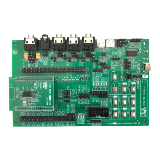
- Page 4 RTL8773E Motherboard User Guide Figure 1-1 the Frames of RTL8773E Motherboard Figure 1-2 the Physical Map of RTL8773E Motherboard & EVB ·Copyright 2019 Realtek Semiconductor Corporation. All Rights Reserved.
- Page 5 RTL8773E Motherboard User Guide Figure 1-3 RTL8773E EVB Daughter board USB Connector CON2 Supply power for RTL8773E VDD_ADP and audio power amplifier. DM and DP signals are connected to VDD_ADP. Li-ion BAT Connector Supply power from external Lithium battery for RTL8773E VBAT.
- Page 6 31. Control jumper for thermal detector J5 32. Power Supply for other device 33. Power supply for other device 34. Jumper for MIC module, J20 35. Power supply for FT 232, J33 36. RTL8773E EVB Daughter board USB Connector USB Power Jumper Description V_5V...
- Page 7 RTL8773E Motherboard User Guide Power test jumper VACC Test Jumper Description Description VDD_ADP VACC Description Description VDD_IO_AUX2 VDD_IO_AUX1 VDD_LDO_AUX2 VDD_LDO_AUX1 Description Description Description AUXIN_L AUXIN_R VDD_DET JACK_L JACK_R MIC1 Jack MIC1 Jack Jumper J23 Jumper J25 Description Description MIC1_N MIC1_P...
- Page 8 RTL8773E Motherboard User Guide MIC2_N Pull Down MIC2_P BIAS Jumper J15 Jumper J19 Description Description MIC_BIAS MIC2_N_DN MIC2_P_UP MIC2 Jack MIC2 Jack Jumper J27 Jumper J29 Description Description MIC1_N MIC1_P JACK_P JACK_N MIC3_N Pull Down MIC3_P BIAS Jumper J26 Jumper J28...
- Page 9 RTL8773E Motherboard User Guide Description Description +OUT_L +OUT_R -OUT_L -OUT_L LOG TP6 Description Description M2_0 RXD_IN TXD_OUT HCI Interface Description RX_IN TX_OUT KEYS&LEDs control jumper 18 19 8 10 Description Description Description KEY0 M1_1 KEY1 M1_2 KEY2 M1_4 KEY3 M1_5...
- Page 10 RTL8773E Motherboard User Guide KEYs&LEDs control jumper 8 10 14 15 Description Description Description LED6 M2_4 LED5 M2_3 LED4 M1_3 LED3 M2_1 KEY3 LED2 M1_0 KEY2 LED1 M0_1 KEY1 IO jumper Audio control jumper 8 10 14 16 18 20 22 24 26...
- Page 11 VDD102 1.4 IO Pins Assignment The RTL8773E Motherboard is designed to fit RTL8773E EVB daughter board. All common interfaces installed on evaluation board are available to each IO pin of RTL8773E chip by connecting control jumpers to different RTL8773E chip’s IOs.
- Page 12 RTL8773E Motherboard User Guide M2_2 M2_2/LED11&KEY7 M2_3 M2_3/LED5 M2_4 M2_4/LED6 M2_5 M2_5 M2_6 M2_6/SPDIF M2_7 M2_7/INS_DET M3_0 M3_0/LED9&KEY5 M3_1 M3_1/LED10&KEY6 M3_2 M3_2/JTAG_nTRST M3_3 M3_3/JTAG_TDI M3_4 M3_4/JTAG_TMS M3_5 M3_5/JTAG_TCK M4_0 M4_0/AMP_EN M4_1 M4_1/KEY4 AUX_R AUX_R AUX_L AUX_L MIC1_P MIC1_P MIC1_N MIC1_N...
- Page 13 RTL8773E Motherboard User Guide P0_2 (ADC_2) P0_2 (ADC_2) M0_2 (ADC2) M0_3 (ADC3) P0_3 (ADC_3) P0_3 (ADC_3) P2_1 P0_0 (ADC_0) P2_1 P2_1 P2_2 P0_1 (ADC_1) P2_2 P2_2 P2_3 P0_0 (ADC_0) P2_4 P0_1 (ADC_1) Please ensure the version of the received daughter board with RTK FAE before using ·Copyright 2019 Realtek Semiconductor Corporation.
-
Page 14: Getting Start
Short jumper J42, then LED7 is on and USB_5V from micro-USB connector CON2 on the front side of the board starts to supply power for RTL8773E Motherboard and EVB. OR connect VADP of jumper J42 to U_5V_FT (TP25), micro-USB connector CON3 on the opposite side of the board starts to supply power for RTL8773E Motherboard and EVB. - Page 15 RTL8773E Motherboard User Guide Figure2-1 Power Jumper Connection 2.2.2 LDO_AUX Setting 8763E LDO_HV33 (VDDIO0) is 3.3V fixed, and it is marked as VDDIO1 or VIO1 on EVB motherboard. LDO_AUX (VDDIO1) is 1.8V by default, and it is marked as VDDIO2 or VIO2 on EVB motherboard. LDO_AUX voltage is adjustable and the customer is allowed to adjust LDO_AUX voltage using McuConfigTool.
- Page 16 RTL8773E Motherboard User Guide we should match power voltage of device with IO voltage. IO Group IC power domain EVB mark Voltage P0_x LDO_AUX VDDIO2 1.8V/3.3V P1_x LDO_HV33 VDDIO1 3.3V P2_x LDO_AUX VDDIO2 1.8V/3.3V P3_x LDO_HV33 VDDIO1 3.3V For example, when using P0_0/P0_1 as data uart, we need to connect with USB to UART converter.
-
Page 17: Debug Interface
RTL8773E Motherboard User Guide In application case, as G-sensor/P-sensor/Light sensor is powered by LDO_HV33 in reference design, please make sure LDO_AUX is configured to be 3.3V. 2.2.3 Debug Interface 2.2.3.1 Download To download and debug APP program, 2 different cases are as follows: J-Link is connected to corresponding SWD interface on motherboard as shown as follows. - Page 18 RTL8773E Motherboard User Guide jumper in J-link, and connect VDDIO1 which is powered through J32 to VCC pin of J-link (Pin1). Figure 2-2 SWD interface connection When using RTK MPPG tool to download, built-in FT232 chip can be adopted as USB to UART convertor.
- Page 19 RTL8773E Motherboard User Guide Figure 2-4 MPPG tool downloading connection 2.2.3.2 LOG In boot code, M2_0 is configured to transmit asynchronous data output as debugging log information in UART protocol. To use FT232 on EVB for log: i. Firstly, please make sure pull off all the jumpers between J40 and J41.
-
Page 20: Keys And Leds
The default mapping table for LEDs and KEYs is shown as Table2-1. Control pins of Keys and LEDs on J3、J6、J44 and J45 can be connected to different RTL8773E Motherboard IOs. For example, Key0’s control pin on J6 is Pin2. By putting jumper wire on J6.1 and J6.2, we can read key value through M1_1. -
Page 21: Audio Interface
Figure 2-7 Active-high KEYs & Active-low KEYs 2.2.5 Audio Interface Aux line-in, dual microphones, and headphone out are supported on RTL8773E Motherboard. When MIC1 jack is used for electret condenser microphone input, follow the steps: Short J22 and J24, as shown in red rectangle box. - Page 22 RTL8773E Motherboard User Guide Figure 2-9 MIC2 connections for condenser microphone MIC3 jack is used for microphone input. When used as electret condenser microphone input, follow the steps: Short J26 and J28. Connect J29.1 with term 1(+) of microphone. Connect J27.1 with term 2(-) of microphone as shown below. MIC3 interface begins to sample voice signal through external microphone.
- Page 23 RTL8773E Motherboard User Guide Short J12, and connect J9.3 with J9.2. SPKL_N and SPKR_N are connected together to U3.1 for differential line. Short J8 and J13. SPKL_P and SPKR_P are transmitted to daughterboard directly. Figure 2-12 Capless connection for Headphone out ALC105 works on motherboard as audio power amplifier.
-
Page 24: Performance Test
RF performance test 3.1 Power Consumption Test Users can perform power consumption test on RTL8773E Motherboard. Users are required to comply with the steps and requirements introduced by this document. 3.1.1 Test Device - This demonstration requires DC source and high-performance current meter. - Page 25 The following are the steps to perform the demonstration: Download RWS flash code to RTL8773E Motherboard with MP Programming Tool. In RWS application, headphone out is configured to be mono .
- Page 26 Figure 3-3 Setting on Agilent 14564B Software and DMM Software 3.2 RF Performance Test In this demonstration, users can perform RF test on RTL8773E Motherboard. Users should comply with the steps and requirements mentioned in this document. After finishing setting up hardware connection, use RF test tool “RTLBTAPP” for non-link test and DUT test mode selection.
- Page 27 RTL8773E Motherboard User Guide 3.2.2 BLE Direct Test Mode - Test RTL8773E Motherboard for BLE Test Item through HCI UART Interface This part describes the direct test mode (DTM) mechanisms for testing BLE items and explains how the direct test mode connection is established.
- Page 28 USB Cable USB to UART converter RF Cable Figure 3-7 Converter for USB to UART RTL8773E Motherboard defines the UART pin as shown in the table below: Table 3-1 HCI UART Pin Define PIN Name Interface HCI UART RX...
- Page 29 This part describes how to establish hardware connection for BR/EDR items or LE RF certification. BR/EDR test requires command from PC through HCI UART. RTL8773E EVB Motherboard use RF path to connect with the Bluetooth measurement instrument as shown in Figure 3-9.
- Page 30 RTL8773E Motherboard User Guide 3. Connect USB connector (blue rectangle in Figure3-9) to PC. 4. Open RF Test tool “RTLBTAPP”, start test according to RF test tool user guide. ·Copyright 2019 Realtek Semiconductor Corporation. All Rights Reserved.
Need help?
Do you have a question about the RTL8773E and is the answer not in the manual?
Questions and answers