
Summary of Contents for XJTAG XJAccelerator
- Page 1 XJTAG ® XJAccelerator Hardware User Guide Version 2 XJTAG-XACC-Guide-24A-05.4 enquiries@xjtag.com www.xjtag.com...
-
Page 2: Table Of Contents
Figure 6 – Rotary switches and connectors....................7 Figure 7 – TDO Routing ...........................8 Figure 8 – Locating the Links to Configure Passthrough Mode..............9 Figure 9 – XJAccelerator with 3 protection boards .................10 Table 1 – XJLink2 Input Connector Pinout....................5 Table 2 – P2 I/O Pinout ..........................6 Table 3 –... -
Page 3: Introduction
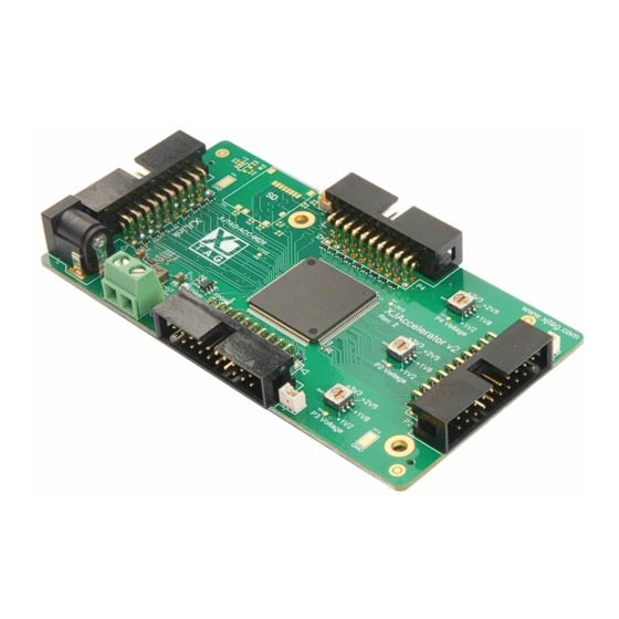
XJAccelerator Hardware . User Guide www.xjtag.com 1. Introduction The XJAccelerator is a configurable FPGA board with three I/O connectors that can run on different voltage domains. The board’s main uses are: • high-speed programming of flash memories when a PCB doesn’t have a suitable FPGA for accelerated programming. -
Page 4: Xjaccelerator Block Diagram
TRISTATE FPGA FPGA configured Figure 2 – XJAccelerator Block Diagram 3. Powering the XJAccelerator The board can be powered from either a DC input socket or screw down terminals. In either case, the input voltage must be between 5 and 12 V DC. -
Page 5: Xjlink2 Connector Pinout (P1)
XJAccelerator Hardware . User Guide www.xjtag.com 4. XJLink2 Connector Pinout (P1) The XJLink2 connects to the board using P1. The JTAG interface and this connector’s PIO operate at 3.3 V, which cannot be changed. The pinout is shown in Table 1. -
Page 6: I/O Pinout
XJAccelerator Hardware . User Guide www.xjtag.com 6. I/O Pinout FPGA Pin FPGA Pin Connector Pin (bank 0) Connector Pin (bank 0) Table 2 – P2 I/O Pinout FPGA Pin FPGA Pin Connector Pin (bank 1) Connector Pin (bank 1) Table 3 – P3 I/O Pinout... -
Page 7: I/O Voltage Domains
XJAccelerator Hardware . User Guide www.xjtag.com 7. I/O Voltage Domains The three I/O connectors can have their voltages configured independently to match the I/O standard required. These voltages provided by the hardware are adjusted by changing the rotary switches near the connectors, as shown in Figure 6. -
Page 8: Setting The I/O Into A Tristate Condition
The TDO signal can be returned to the XJLink2 either directly from the FPGA’s JTAG port (e.g. when using the XJAccelerator for programming) or from the FPGA’s internal logic (e.g. when using it as a JTAG multiplexer) as shown in Figure 7. -
Page 9: Passthrough Mode
11. Passthrough Mode The XJAccelerator can be configured in hardware so that some of the signals to/from the XJLink2 are routed directly to connectors P2 and P3. This can be used, for example, to utilise the XJLink2’s frequency or analogue voltage measuring capabilities. -
Page 10: Programming Fpga Images
3. If the FPGA is unprogrammed or does not contain the expected image, automatically program the on-board flash with the required image and then force the FPGA to reload from it. XJTAG can supply the XJAccelerator together with an XJDeveloper board file and the associated XJEase files to provide this functionality.
Need help?
Do you have a question about the XJAccelerator and is the answer not in the manual?
Questions and answers