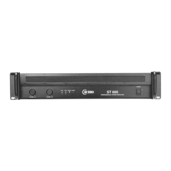
Summary of Contents for C-Audio ST Series
- Page 5 NOTE CMRR CIRCUIT SHOWN APPLIES TO ST600 FOR ST400 TR4 & TR8 ARE NOT FITTED AND WIPER R10 = 12k I/P - A 120k R19 & R20 = 30k 100u 220R 100u I/P + A BRIDGE OUT 110k 0dB Sensitivity Modification IC1A BOTTOM Change R5 from 3k3 to 6k65...
- Page 6 NOTE CMRR CIRCUIT DIAGRAM SHOWN APPLIES TO ST600 STEREO BRIDGE FOR ST400 : WIPER TR14 & TR18 ARE NOT FITTED I/P - B 120k R46 = 12k R55 & R56 = 30k 100u 220R 100u I/P + B 0dB Sensitivity Modification IC3B BOTTOM Change R41 from 3k3 to 6k65...
- Page 7 RLY CONT A 470k THERMAL/A 220k 112 C IN4148 IN4148 IC5B IN4148 LM339 TR21 IC5A 470k 470k BC214L LM339 MON A PEAK A IN4148 IN4148 470n 470n 100p 470k 470k THERMAL A SEE NOTE RLY CONT B ZD10 R100 IC5D IN4148 IN4148 IC5C...
- Page 8 FEEDBACK + MT BRIDGE R80A R85A R17A 3k3/5W C14A 100uF R22A R27A R28A GT1A 100k 330R ZD4A D13A ZD12A BAV21 SC1A ZD8A C29A C15A R21A 100uF C11A 100uF GT2A R83A ZD5A 100R RV1A D11A R66A R70A R72A D25A IN4148 BAV21 IN4148 R64A R14A...
- Page 9 FEEDBACK + MT R17B C14B 100uF R22B R27B R28B GT1B 100k 330R ZD4B D13B ZD12B BAV21 SC1B ZD8B C29B C15B R21B 100uF C11B 100uF GT2B R83B 100R RV1B D11B R66B R70B R72B IN4148 BAV21 ZD5B R64B R14B 150R R20B D25B C54B 120k C17B...
- Page 10 + HT DRAWING OF OUTPUT STAGE COMPONENT REFERENCES SHOULD BE SUFFIXED WITH A OR B FOR RESPECTIVE CHANNELS 560R 560R 560R 560R K1058 K1058 K1058 K1058 BYT30P400 + MT Cmod1 Cmod2 100n 2.5W 560R 560R 560R 560R K1058 K1058 K1058 K1058 TR10 TR11...
- Page 11 + HT + HT BR1B BR2A SB5006 SB5006 9000uF 9000uF ACH(B) ACH(B) ACH(A) ACH(A) + MT + MT FEEDBACK FEEDBACK 9000uF 9000uF 2.5W 2.5W BR2B OUTPUT B BR1A OUTPUT A SB5006 RL1B SB5006 RL1A ACL(B) ACL(B) ACL(A) ACL(A) 2.5W 2.5W 9000uF 2.5W 2.5W...
- Page 12 R53A + MT C27B R61B CHANNEL A R54A R56A 470k THERMAL/A RL1A - MT 220k RELAY IN4148 112 C ZD3A IN4148 IN4148 R57A R60A IC1D LM339 IN4148 TR17A IC1C BC214L LM339 R52A CHAN A PEAK A R48A IN4148 OUTPUT IN4148 C26A C28A CN1.1...
- Page 13 ST Series Modification Procedure General The following changes are to be made to All ST amplifiers irrespective of Issue : 1) Remove C20 & C28 (10pF) from the PCB and replace with 15pF, 50V ceramic capacitors. 2) Remove C10 & C32 (47pF) from the PCB and replace with 100pF, 50V ceramic capacitors.
- Page 14 Procedure 1 Issue 6 PCBs 1) Remove R17, R22, R53 & R58 (5k6) from the PCB and replace with 5k1, 1/4W. 2) Remove R18, R21, R54 & R57 (1k8) from the PCB and replace with 5k1, 1/4W. 3) Remove ZD1, ZD2, ZD3 & ZD4 (12V) from the PCB and replace with 9V1 1/2W. 4) Fit 390k, 1/4W resistor solder-side between D40 Cathode and D41 Anode, as per figure 2.
- Page 15 Procedure 2 Issue 4 & 5 PCBs with Modification Daughter Boards 1) Remove R17, R22, R53 & R58 (5k6) from the PCB and replace with 5k1, 1/4W. 2) Remove ZD1, ZD2 & ZD3 (12V) from the PCB and replace with 9V1 1/2W. 3) Fit 9V1, 1/2W zener diode solder-side in position ZD4 as per figure 3.
- Page 16 1) Remove R17, R22, R53 & R58 (5k6) from the PCB and replace with 5k1, 1/4W. 2) Remove R18, R21, R54 & R57 (1k8) from the PCB and replace with 5k1, 1/4W. 3) Remove ZD1, ZD2, ZD3 & ZD4 (12V) from the PCB and replace with 9V1 1/2W. 4) Fit 390k, 1/4W resistor between Component Network diodes as per figure 5.
-
Page 17: General Notes
1) Remove R17, R22, R53 & R58 (5k6) from the PCB and replace with 5k1, 1/4W. 2) Remove R18, R21, R54 & R57 (1k8) from the PCB and replace with 5k1, 1/4W. 3) Remove ZD1, ZD2, ZD3 & ZD4 (12V) from the PCB and replace with 9V1 1/2W. 4) Remove Components fitted in positions R19, R20, R55 &... - Page 18 Once the appropriate modifications have been carried out it is recommended that the following checks are performed before attempting to re-test the amplifier. 1) Output Stage : Check for faulty Output transistors in the following way : a) Measure between Drain and Source of each transistor with a multi-meter set on a low Ohms range.


Need help?
Do you have a question about the ST Series and is the answer not in the manual?
Questions and answers