Table of Contents
Advertisement
Quick Links
Advertisement
Table of Contents

Subscribe to Our Youtube Channel
Related Manuals for Sylvania Emerson 6427FD/EWF2703


Summary of Contents for Sylvania Emerson 6427FD/EWF2703
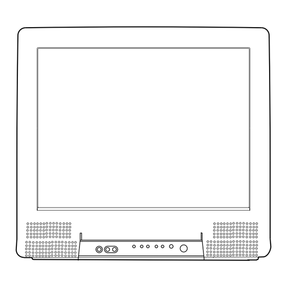
- Page 1 SERVICE MANUAL 27" COLOR TELEVISION 6427FD/EWF2703...
-
Page 2: Table Of Contents
IMPORTANT SAFETY NOTICE Proper service and repair is important to the safe, reliable operation of all Funai Equipment. The service procedures recommended by Funai and de- scribed in this service manual are effective methods of performing service operations. Some of these service special tools should be used when and as recommended. -
Page 3: Specifications
SPECIFICATIONS <TUNER> ANT. Input ------------------- 75ohm Unbal., F type Reference Level ----------- 20Vp-p (CRT Green Cathode) Test Input Signal ---------- 400Hz 30% modulation Description Condition Unit Nominal Limit 1. Intermediate Freq. Picture 45.75 Sound 41.25 2. Peak Picture Sens dBµv CATV dBµv dBµv... -
Page 4: Important Safety Precautions
IMPORTANT SAFETY PRECAUTIONS Prior to shipment from the factory, our products are strictly inspected for recognized product safety and electrical codes of the countries in which they are to be sold. However, in order to maintain such compliance, it is equally important to implement the following precautions when a set is being serviced. - Page 5 ing is performed that involves B+, horizontal de- earth ground. If a voltage reading in excess of 1.0V flection or high voltage. Correct operation of the X- is obtained, remove and reinsert the AC power radiation protection circuits also must be recon- plug in the opposite polarity and again measure firmed each time they are serviced.
- Page 6 Precautions during Servicing 3) Align the lengths of the wires to be connected. In- sert the wires fully into the connector. A. Parts identified by the ( # ) symbol are critical for 4) Use the crimping tool to crimp the metal sleeve at safety.
- Page 7 Safety Check after Servicing Examine the area surrounding the repaired location Chassis or Secondary Conductor for damage or deterioration. Observe that screws, parts and wires have been returned to original posi- tions. Afterwards, perform the following tests and con- Primary Circuit Terminals firm the specified values in order to verify compliance with safety standards.
-
Page 8: Standard Notes For Servicing
STANDARD NOTES FOR SERVICING Circuit Board Indications (2) Remove the flat pack-IC with tweezers while ap- plying the hot air. a. The output pin of the 3 pin Regulator ICs is indicat- (3) Bottom of the flat pack-IC is fixed with glue to the ed as shown. - Page 9 With Soldering Iron: soldering iron to center of the flat pack-IC and heat up. Then remove (glue will be melted). (Fig. S-1-6) (1) Using desoldering braid, remove the solder from all pins of the flat pack-IC. When you use solder (5) Release the flat pack-IC from the CBA using twee- flux which is applied to all pins of the flat pack-IC, zers.
- Page 10 2. Installation Instructions for Handling Semiconductors (1) Using desoldering braid, remove the solder from the foil of each pin of the flat pack-IC on the CBA Electrostatic breakdown of the semiconductors may so you can install a replacement flat pack-IC more occur due to a potential difference caused by electro- easily.
-
Page 11: Disassembly Instructions
CABINET DISASSEMBLY INSTRUCTIONS 1. Disassembly Flowchart Note : (1) Order of steps in procedure. When reassembling, This flowchart indicates the disassembly steps for the follow the steps in reverse order.These numbers cabinet parts, and the CBA in order to gain access to are also used as the Identification (location) No. - Page 12 Front Cabinet [3] Main CBA Control Plate [1] Rear Cabinet Fig. 1 Fig. 3 Anode Cap Degaussing Coil Ground Wire [2] CRT [1] Rear Cabinet Front Cabinet Front Cabinet [4] CRT Control Plate Control Plate Fig. 4 Fig. 2 L6610DC...
- Page 13 TV Cable Wiring Diagram SP802 SP801 L691 DEGAUSSING COIL CLN802 CLN801 MAIN CBA CN801 CN802 WH301A CN691 FLYBACK TRANSFORMER TUNER T571 WH501A CN571 AC601 AC CORD FOCUS SCREEN WH301B WH501B ANODE CN1501 Fig. 5 TO CRT GROUND L6610DC...
-
Page 14: Electrical Adjustment Instructions
ELECTRICAL ADJUSTMENT INSTRUCTIONS How to set up the service mode: General Note: "CBA" is abbreviation for "Circuit Board Assem- Service mode: bly." 1. Use the service remote control unit. NOTE: 2. Turn the power on. (Use main power on the TV Electrical adjustments are required after replacing unit.) circuit components and certain mechanical parts. - Page 15 2. Initial Setting S-CLR 1. Press "MENU" button on the service remote con- General trol unit. Then select "S-COLOR" (S-CLR) display. 1. Enter the Service mode. (See page 5-1) 2. Press "CH o/p" buttons on the service remote 2. Press "VOL p" button on the service remote control control unit so that the value of "S-COLOR"...
- Page 16 5. Purity Check C-SRP 1. Press "MENU" button on the service remote con- 1. Enter the Service mode. (See page 5-1) trol unit. Then select "COMPONENT SHARP- 2. Press "7" button on the remote control unit. Each NESS" (C-SRP) display. time pressing 7"...
- Page 17 7. H. Position Adjustment 9. V. Position Adjustment Purpose: To obtain correct horizontal position of Purpose: To obtain correct vertical width of screen image. screen image. Symptom of misadjustment: If V. Position is incor- Symptom of Misadjustment: If H. Position is incor- rect, vertical height of image on the screen may not be rect, horizontal position of image on the screen may properly displayed.
- Page 18 12. Software Reset 15. Cut-off Adjustment Purpose: To adjust the beam current of R, G, B, and To reset software, press “5” button on the remote con- screen voltage. trol unit for at least 5 seconds after pressing “CH RETURN” button on the remote control unit. Symptom of Misadjustment: White color may be reddish, greenish or bluish.
- Page 19 16. White Balance Adjustment 17. Sub-Brightness Adjustment Purpose: To mix red, green and blue beams correctly Purpose: To get proper brightness. for pure white. Symptom of Misadjustment: If Sub-Brightness is Symptom of Misadjustment: White becomes bluish incorrect, proper brightness cannot be obtained by or reddish.
- Page 20 21. Convergence Adjustment The following adjustments normally are not attempted in the field. Only when replacing the Purpose: To obtain proper convergence of red, green CRT then adjust as a preparation. and blue beams. 19. Purity Adjustment Symptom of Misadjustment: If Convergence Adjust- ment is incorrect, the edge of white letters may have Purpose: To obtain pure color.
- Page 21 22. Yh, Yv, Xv Adjustment 1. Adjust the volume of Deflection Yoke(Yh, Yv, Xv) to get good convergence. FRONT L6610EA...
-
Page 22: Block Diagram
BLOCK DIAGRAMS System Control Block Diagram IC333 TV MICON/VIDEO /AUDIO/CHROMA /DEFLECTION RCV101 REMOTE RCV-IN SENSOR (NO CONNECTION) CN301 I2C-OPEN KEY-IN1 SWITCH KEY-IN2 CN301 is used for adjustment at factory INPUT0 IC151 IF/VIDEO BLOCK (MEMORY) 72 I2C-OPEN SCL 6 SDA 5 FROM/TO INPUT0 Q141... - Page 23 IF/Video Block Diagram RF/IF SIGNAL VIDEO SIGNAL AUDIO SIGNAL IC33 (IF SIGNAL PROCESS) MAIN CBA CF31 VIDEO 4.5MHz FILTER TRAP CF32 4.5MHz AUDIO BLOCK FILTER EXT.CLK VCO F/B WF16 IF AGC DET FROM/TO INPUT0 SYSTEM CONTROL BLOCK IC333 TV MICON/VIDEO /AUDIO/CHROMA /DEFLECTION JK721...
- Page 24 Audio Block Diagram AUDIO SIGNAL IC431 (MTS/SAP AUDIO SIGNAL PROCESS) MAIN CBA FROM STEREO 75uS L-CH OFFSET IF/VIDEO BLOCK FILTER FILTER DE-EMPH CANCEL OFFSET CANCEL MATRIX FILTER R-CH WIDE BAND WIDE BAND WIDE BAND OFFSET (L-R)/SAP FILTER RMS DET EXPAND CANCEL SAP OUT FILTER...
- Page 25 CRT/H.V. Block Diagram VIDEO SIGNAL IC551 (V-DEFLECTION CONTROL) MAIN CBA WF12 THERMAL L551 D.Y. WF11 PROTECTION RAMP-OUT DRIVE P-ON-H Q531 (SWITCHING) PULSE V-RAMP-F/B DRIVE Q551, Q552 CONTROL FROM/TO IF/VIDEO BLOCK CN551 Q561 Q533 (SWITCHING) SWITCHING Q572 Q571 T572 VR561 VR562 P-ON-ON H-DRIVE H.DRIVE...
- Page 26 Power Supply Block Diagram CAUTION ! Fixed voltage ( or Auto voltage selectable ) power supply circuit is used in this unit. If Main Fuse (F601) is blown, check to see that all components in the power supply CAUTION: FOR CONTINUED PROTECTION AGAINST RISK OF FIRE, NOTE : circuit are not defective before you connect the AC plug to the AC power supply.
-
Page 27: Schematic Diagram / Cba's And Test Points
SCHEMATIC DIAGRAMS / CBA'S AND TEST POINTS Standard Notes Many electrical and mechanical parts in this chassis have special characteristics. These characteristics often pass unnoticed and the protection afforded by them cannot necessarily be obtained by using replacement compo- nents rated for higher voltage, wattage, etc. Replacement parts that have these special safety characteristics are identified in this manual and its supplements;... - Page 28 LIST OF CAUTION, NOTES, AND SYMBOLS USED IN THE SCHEMATIC DIAGRAMS ON THE FOLLOWING PAGES: 1. CAUTION: FOR CONTINUED PROTECTION AGAINST RISK OF FIRE, REPLACE ONLY WITH SAME TYPE_A,_V FUSE. ATTENTION: UTILISER UN FUSIBLE DE RECHANGE DE MÊME TYPE DE_A,_V. 2.
- Page 29 Main 1/4 Schematic Diagram VIDEO SIGNAL MAIN 1/4 Ref No. Position IC151 IC333 TRANSISTORS Q111 Q131 Q141 Q191 Q321 CONNECTOR CN301 L6610SCM1...
- Page 30 Main 2/4 Schematic Diagram VIDEO SIGNAL AUDIO SIGNAL MAIN 2/4 Ref No. Position IC431 IC771 IC801 TRANSISTORS Q702 Q751 Q761 Q791 Q792 Q793 Q794 Q825 Q831 Q832 Q841 Q851 Q951 Q956 Q961 CONNECTORS CN801 CN802 L6610SCM2...
- Page 31 Main 3/4 Schematic Diagram CAUTION ! IF SIGNAL CAUTION: FOR CONTINUED PROTECTION AGAINST RISK Fixed voltage ( or Auto voltage selectable ) power supply circuit is used in this unit. NOTE : OF FIRE, REPLACE ONLY WITH SAME TYPE 4A, 125V FUSE. VIDEO SIGNAL If Main Fuse (F601) is blown, check to see that all components in the power supply The voltage for parts in hot circuit is measured...
- Page 32 Main 4/4 & CRT Schematic Diagram MAIN 4/4 Ref No. Position Ref No. Position Ref No. Position Ref No. Position TRANSISTORS TEST POINTS TRANSISTORS IC551 Q571 TP591 Q1511 TRANSISTORS TP592 Q572 Q1512 CONNECTORS Q531 TP601 Q1521 VARIABLE RESISTORS Q533 CN571 Q1522 WH301A VR561...
- Page 33 Main CBA Top View CAUTION ! BECAUSE A HOT CHASSIS GROUND IS PRESENT IN THE POWER CAUTION: FOR CONTINUED PROTECTION AGAINST RISK Fixed voltage ( or Auto voltage selectable ) power supply circuit is used in this unit. SUPPLY CIRCUIT, AN ISOLATION TRANSFORMER MUST BE USED. OF FIRE, REPLACE ONLY WITH SAME TYPE 4A, 125V FUSE.
- Page 34 Main CBA Bottom View CAUTION: FOR CONTINUED PROTECTION AGAINST RISK CAUTION ! BECAUSE A HOT CHASSIS GROUND IS PRESENT IN THE POWER OF FIRE, REPLACE ONLY WITH SAME TYPE 4A, 125V FUSE. Fixed voltage ( or Auto voltage selectable ) power supply circuit is used in this unit. SUPPLY CIRCUIT, AN ISOLATION TRANSFORMER MUST BE USED.
- Page 35 CRT CBA Top View CRT CBA Bottom View CRT CBA Ref No. Position TRANSISTORS Q1511 Q1512 Q1521 Q1522 Q1531 Q1532 CONNECTORS CN1501 WH301B WH501B TEST POINTS TP500 TP501 WF15 WF14 WF13 Q1511 Q1511 Q1521 Q1521 Q1531 Q1531 Collector Base Base Collector Base Collector...
-
Page 36: Waveforms
WAVEFORMS Input: NTSC Color Bar Signal (with 1kHz Audio Signal) INITIAL POSITION: Unplug unit from AC outlet for at least 5 minutes. reconnect to AC outlet and then turn power on. WF1 ~ WF16 = Waveforms to be observed at (Brightness---Center Color---Center Tint --- Center Contrast---Approx 70%) Waveform check points. -
Page 37: Wiring Diagram
WIRING DIAGRAM CN801 CLN801 1 SP-L SP801 SP-GND SPEAKER L-CH CN802 CLN802 1 SP-R SP802 SP-GND SPEAKER R-CH ANODE TU1 TUNER UNIT V501 MAIN CBA BL6650F01011-1 CN691 FOCUS CN1501 T571 SCREEN WH301B WH301A CLN301 BLUE BLUE GREEN GREEN WH501B WH501A CLN501 CRT CBA HEATER 3... -
Page 38: Ic Pin Function
IC PIN FUNCTIONS IC333 (TV Micro Computer) Signal Name Function Signal Name Function 35 N.U. Not Used 36 N.U. Not Used 37 V RAMP F/B V Ramp Feed Back N.U. Not Used 38 V RAMP OUT Vertical Output N.U. Not Used 39 V RAMP CAP V Ramp OSC Capacitor N.U. - Page 39 Signal Name Function 70 RCV-IN Input For Remote Control 71 N.U. Not Used White Balance Adjustment 72 I2C OPEN Judgement 73 AFT AFT Voltage Input 74 DG-ON-H Degaussing Coil Control 75 AGC AGC Voltage Input 76 PROTECT 3 Power Supply Protection 77 N.U.
- Page 40 EXPLODED VIEWS Cabinet SHINWHA V501-1 TAPE SGT-730 Details for DY551 (L551) (BLACK) and surrounding parts V501-2 SHINWHA TAPE SGT-730 L-10 B-11 (WHITE) DY551 (L551) Scotch Tape #880 B-20 CLN551 DY551 (L551) CRT CBA B-11 B-20 L691 B-20 L-13 SP801 V501 L-13 L-13 B-20...
- Page 41 Packing TAPE PACKING TAPE S7 (EWF2703 only) PACKING TAPE 11-3 L6610PEX...
-
Page 42: Mechanical Parts List
MECHANICAL PARTS LIST PRODUCT SAFETY NOTE: Products marked with a # Ref. No. Description Part No. have special characteristics important to safety. Before DRY BATTERY R6P UM3 or XB0M451GH001 replacing any of these components, read carefully the DRY BATTERY R6P/2S or XB0M451T0001 product safety notice in this service manual. - Page 43 Table 1 (V501 and DY551 (OR L551) Combi- nation) Note 1: Purity and Convergence Adjustments must be performed following CRT replacement. Refer to Electri- cal Adjustment Instructions. Note 2: Please confirm CRT Type No. on the CRT Warning Label which is located on the CRT. Then See the Table 1 for V501 and DY551 (OR L551) combina- tion chart.
-
Page 44: Electrical Parts List
ELECTRICAL PARTS LIST PRODUCT SAFETY NOTE: Products marked with a Ref. No. Description Part No. # have special characteristics important to safety. ELECTROLYTIC CAP. 0.47µF/50V M CE1JMASDLR47 Before replacing any of these components, read care- ELECTROLYTIC CAP. 4.7µF/50V M or CE1JMASTL4R7 fully the product safety notice in this service manual. - Page 45 Ref. No. Description Part No. Ref. No. Description Part No. C322 ELECTROLYTIC CAP. 0.47µF/50V M or CE1JMASTLR47 C429 ELECTROLYTIC CAP. 1µF/50V M or CE1JMASTL1R0 ELECTROLYTIC CAP. 0.47µF/50V M CE1JMASDLR47 ELECTROLYTIC CAP. 1µF/50V M or CE1JMASTL010 C323 ELECTROLYTIC CAP. 0.1µF/50V M or CE1JMASTLR10 ELECTROLYTIC CAP.
- Page 46 Ref. No. Description Part No. Ref. No. Description Part No. PP CAP. 0.0022µF/1.6KV J CT3C222MS039 CERAMIC CAP. 0.0047µF F CS CCG2HMN0F472 C568 FILM CAP.(P) 0.033µF/50V J or CMA1JJS00333 C650 CERAMIC CAP. LB 560pF/2KV or CA3D561KG004 FILM CAP.(P) 0.033µF/50V J or CA1J333MS029 CERAMIC CAP.
- Page 47 Ref. No. Description Part No. Ref. No. Description Part No. ELECTROLYTIC CAP. 1µF/50V M CE1JMASDL010 C1521 CERAMIC CAP.(AX) B K 470pF/50V CCA1JKT0B471 C757 ELECTROLYTIC CAP. 0.1µF/50V M or CE1JMASTLR10 C1522 CERAMIC CAP.(AX) B K 0.01µF/50V CA1J103TU011 ELECTROLYTIC CAP. 0.1µF/50V M CE1JMASDLR10 C1531 CERAMIC CAP.(AX) B K 470pF/50V...
- Page 48 Ref. No. Description Part No. Ref. No. Description Part No. DIODE 1SS176TPA7 1SS176T FAST RECOVERY DIODE ERB44-02 QDPZ0ERB4402 D547 SWITCHING DIODE 1SS133(T-77) or QDTZ001SS133 D658# DIODE 1ZC18 or QDQZ0001ZC18 SWITCHING DIODE 1N4148 or NDTZ001N4148 ZENER DIODE RD18F QDQZ000RD18F DIODE 1SS176TPA7 1SS176T D660 SWITCHING DIODE 1SS133(T-77) or...
- Page 49 Ref. No. Description Part No. Ref. No. Description Part No. D963 ZENER DIODE MTZJT-775.6B or QDTB0MTZJ5R6 TRANSISTOR 2SC2785(H) or QQSH02SC2785 ZENER DIODE DZ-5.6BSBT265 NDTB0DZ5R6BS TRANSISTOR 2SC2785(J) or QQSJ02SC2785 D966 SWITCHING DIODE 1SS133(T-77) or QDTZ001SS133 TRANSISTOR KTC3199(GR) or NQS10KTC3199 SWITCHING DIODE 1N4148 or NDTZ001N4148 TRANSISTOR KTC3198(GR) or NQS40KTC3198...
- Page 50 Ref. No. Description Part No. Ref. No. Description Part No. TRANSISTOR KTA1266(GR) or NQS40KTA1266 TRANSISTOR KTC3199(GR) or NQS10KTC3199 TRANSISTOR 2SA1318(T)-AANP or 2SA1318TZ TRANSISTOR KTC3198(GR) or NQS40KTC3198 TRANSISTOR 2SA1318(U)-AANP or 2SA1318UZ TRANSISTOR 2SC3331(T)-AANP or 2SC3331TZ TRANSISTOR 2SA1015-GR(TPE2) QQS102SA1015 TRANSISTOR 2SC3331(U)-AANP or 2SC3331UZ Q552# TRANSISTOR KTD2059(O) or...
- Page 51 Ref. No. Description Part No. Ref. No. Description Part No. CARBON RES. 1/4W J 22k Ω TRANSISTOR 2SC3331(U)-AANP or 2SC3331UZ R139 RCX4JATZ0223 CARBON RES. 1/4W J 1k Ω or TRANSISTOR 2SC1815-GR(TPE2) QQS102SC1815 R140 RCX4JATZ0102 CARBON RES. 1/6W J 1k Ω Q851 TRANSISTOR 2SC2120-O-TPE2 or QQS002SC2120...
- Page 52 Ref. No. Description Part No. Ref. No. Description Part No. CARBON RES. 1/4W J 1k Ω or METAL OXIDE FILM RES. 1W J 8.2 Ω or R330 RCX4JATZ0102 R552# RN018R2ZU001 CARBON RES. 1/6W J 1k Ω METAL OXIDE FILM RES. 1W J 8.2 Ω RCX6JATZ0102 RN018R2DP003 CARBON RES.
- Page 53 Ref. No. Description Part No. Ref. No. Description Part No. CEMENT RES. 5W K 0.27 Ω or CARBON RES. 1/6W J 82 Ω R613# RW05R27DP005 RCX6JATZ0820 CEMENT RESISTOR 5W K 0.27 Ω CARBON RES. 1/4W J 82 Ω or RW05R27PG001 R702 RCX4JATZ0820 CARBON RES.
- Page 54 Ref. No. Description Part No. Ref. No. Description Part No. CARBON RES. 1/4W J 10k Ω R772 RCX4JATZ0103 TACT SWITCH SKHHAM SST0101AL029 CARBON RES. 1/4W J 4.7k Ω R791 RCX4JATZ0472 SW104 TACT SWITCH SKQSAB or SST0101AL038 CARBON RES. 1/4W J 4.7k Ω R792 RCX4JATZ0472 TACT SWITCH KSM0612B or...
- Page 55 Ref. No. Description Part No. Ref. No. Description Part No. JS104 PCB JUMPER D0.6-P5.0 JW5.0T COILS JS105 PCB JUMPER D0.6-P5.0 JW5.0T L1501# INDUCTOR 150µH-J-5FT or LLARJCSTU151 JS171 PCB JUMPER D0.6-P15.0 JW15.0T INDUCTOR 150µH-K LLARKDQKA151 JS191 PCB JUMPER D0.6-P5.0 JW5.0T L1511 PCB JUMPER D0.6-P5.0 JW5.0T JS301...
- Page 56 Ref. No. Description Part No. CARBON RES. 1/6W J 100 Ω RCX6JATZ0101 METAL RESISTOR 3W J 10k Ω or R1520# RN03103ZU001 FIXED METAL OXIDE FILM RES. 3W J 10k Ω RN03103DP005 CARBON RES. 1/4W J 1.5k Ω R1521 RCX4JATZ0152 CARBON RES. 1/4W J 1.5k Ω R1522 RCX4JATZ0152 CARBON RES.
- Page 57 Printed in Japan 2003-05-20 HO...
Need help?
Do you have a question about the Emerson 6427FD/EWF2703 and is the answer not in the manual?
Questions and answers