National Instruments USRP-2950 Getting Started Manual
Hide thumbs
Also See for USRP-2950:
- Getting started manual (34 pages) ,
- Getting started manual (37 pages)
Table of Contents
Advertisement
Quick Links
Advertisement
Table of Contents

Subscribe to Our Youtube Channel
Related Manuals for National Instruments USRP-2950


Summary of Contents for National Instruments USRP-2950
- Page 1 USRP-2950/2952/2953 2022-07-11...
-
Page 2: Table Of Contents
USRP-2950......... -
Page 3: Usrp Rio Getting Started Guide
Furthermore, any changes or modifications to the product not expressly approved by National Instruments could void your authority to operate it under your local regulatory rules. © National Instruments... -
Page 4: Verifying The System Requirements
USRP-2950/2952/2953/2954/2955 Verifying the System Requirements To use the NI-USRP instrument driver, your system must meet certain requirements. Refer to the product readme, which is available online at ni.com/manuals, for more information about minimum system requirements, recommended system, and supported application development environments (ADEs). - Page 5 In addition to the kit contents, you must provide the following additional item(s): An MXI Express interface card. You can purchase an MXI Express interface kit ■ for your USRP RIO device, which contains an MXI Express interface card, at ni.com. © National Instruments...
-
Page 6: Preparing The Environment
USRP-2950/2952/2953/2954/2955 Optional Items LabVIEW Modulation Toolkit (MT), available for download at ni.com/ ■ downloads and included in LabVIEW Communications System Design Suite, which includes MT VIs and functions, examples, and documentation Note You must install the LabVIEW Modulation Toolkit for proper operation of the NI-USRP Modulation Toolkit example VIs. -
Page 7: Installing The Software
Install all the software you plan to use before you install the hardware. Ensure that the USRP RIO device and computer are off before installing. 1. Attach the antenna or cable to the front panel terminals of the USRP RIO device as desired. © National Instruments... - Page 8 USRP-2950/2952/2953/2954/2955 2. Use the MXI Express Interface Kit to connect the USRP RIO device to the computer. 1. Identify which MXI Express Interface Kit you want to use. If you are using the desktop connectivity kit or the PXI chassis ■...
-
Page 9: Synchronizing Multiple Usrp Rio Devices (Optional)
CDA-2990 using a standard SMA (m)-to-SMA (m) cable. 3. Repeat steps 1 and 2 to synchronize additional USRP RIO devices using the additional ports on the CDA-2990 (optional). The completed hardware setup for two USRP RIO devices is shown in the following figure. © National Instruments... -
Page 10: Preparing The Usrp-2955 For Lo Sharing (Optional)
USRP-2950/2952/2953/2954/2955 Figure 3. Synchronizing Multiple USRP RIO Devices with the CDA-2990 CDA-2990 10 MHz OUT PPS OUT PPS OUT ETHERNET PRIMARY REF GPS ANT EXT 10 MHz EXT PPS POWER INPUT INPUT INPUT Designed by Ettus Research Designed by Ettus Research... -
Page 11: Ni-Usrp Instrument Driver
Use with the LabVIEW LabVIEW Communications the FPGA of your USRP RIO FPGA Module to customize System Design Suite: device for advanced the behavior of the device Diagram » Hardware FPGA to create Interfaces » USRP RIO © National Instruments... -
Page 12: Ni-Usrp Sample Projects
USRP-2950/2952/2953/2954/2955 Software Description Use Case Palette Location Option programming and digital application-specific LabVIEW: Functions » signal processing (DSP). instrument designs. Instrument I/O » Instrument Drivers » USRP RIO Uses the USRP RIO Sample Projects, which allow you to take common measurements with your device. -
Page 13: Verifying The Device Connection (Optional)
In LabVIEW Communications System Design Suite at Learning » Examples » ■ Hardware Input and Output. From the Start menu at Start » All Programs » National Instruments » NI- ■ USRP » Examples. In LabVIEW from Functions » Instrument I/O » Instrument Drivers »... -
Page 14: Troubleshooting
USRP-2950/2952/2953/2954/2955 Device USRP-2950/2952/2953/2954 Tx and Rx Streaming Host VI USRP-2955 Rx Streaming (Host) VI If the device is transmitting and/or receiving signals, the front panel graphs display waveform data. 4. Click STOP to conclude the test. Troubleshooting If an issue persists after you complete a troubleshooting procedure, contact NI technical support or visit ni.com/support. -
Page 15: Why Don't Ni-Usrp Examples Appear In The Ni Example Finder
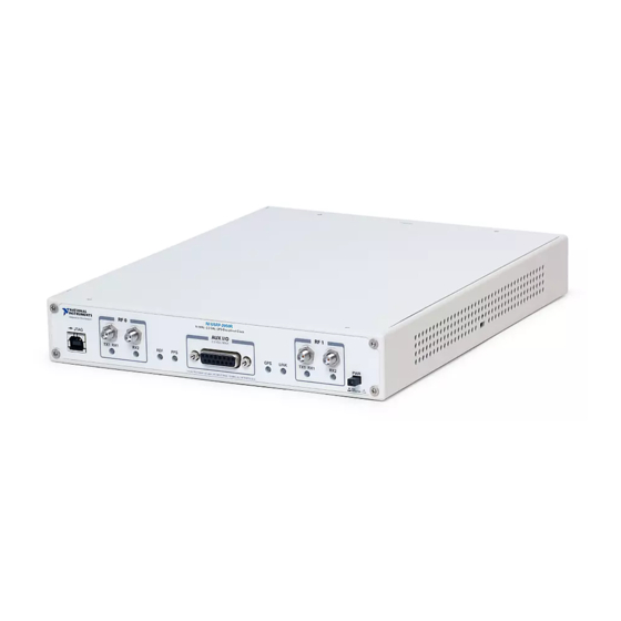
In LabVIEW Communications System Design Suite at Learning » Examples » ■ Hardware Input and Output. From the Start menu at Start » All Programs » National Instruments » NI- ■ USRP » Examples. In LabVIEW from Functions » Instrument I/O » Instrument Drivers »... - Page 16 Input terminal for the RF signal. RX2 is an SMA (f) connector with an impedance of 50 Ω and is a single-ended input channel. Table 15. USRP-2950 Module Front Panel Connectors Note The LED indications described in the following table occur only when you use the NI-USRP API with the default API image.
- Page 17 Indicates the receive status — The module is not receiving. of the module. Green Solid The module is receiving. Table 16. USRP-2950 Module LEDs Figure 6. USRP-2950 Module Back Panel 1G/10G ETH PCIe x4 9-16V DC SFP+Ports TRIG TRIG 7.5 A MAX 3.3 V...
-
Page 18: Usrp-2952
-15 dBm and an output of DC 5 V to power an active antenna. Caution Do not terminate the GPS ANT port if you do not use it. Table 17. USRP-2950 Module Back Panel Connectors USRP-2952 Figure 7. USRP-2952 Front Panel JTAG... - Page 19 Indicates the pulse per — There is no PPS timing reference second (PPS). signal, or the device is not locked to the reference signal. Green Blinking The device is locked to the PPS timing reference signal. © National Instruments...
- Page 20 USRP-2950/2952/2953/2954/2955 Description Color State Indication Indicates whether the — There is no GPSDO or the GPSDO GPSDO is locked. is not locked. Green Solid The GPSDO is locked. LINK Indicates the status of the — There is no link to a host link to a host computer.
-
Page 21: Usrp-2953
50 Ω and is a single-ended input or output channel. Input terminal for the RF signal. RX2 is an SMA (f) connector with an impedance of 50 Ω and is a single-ended input channel. Table 15. USRP-2953 Module Front Panel Connectors © National Instruments... - Page 22 USRP-2950/2952/2953/2954/2955 Note The LED indications described in the following table occur only when you use the NI-USRP API with the default API image. When you use LabVIEW FPGA, you customize the LED indications. Description Color State Indication RF 0 TX1 Indicates the transmit status —...
- Page 23 (TRIG IN) that you control using NI-USRP software. GPS ANT Input terminal for the GPS antenna signal. GPS ANT is a female SMA connector with a maximum input power of -15 dBm and an output of DC 5 V to power an active antenna. © National Instruments...
-
Page 24: Usrp-2954
USRP-2950/2952/2953/2954/2955 Connector Caution Do not terminate the GPS ANT port if you do not use it. Table 17. USRP-2953 Module Back Panel Connectors USRP-2954 Figure 11. USRP-2954 Front Panel NI USRP-2954R RF 0 RF 1 10 MHz - 6 GHz, GPS-Disciplined Clock (160 MHz BW) - Page 25 The module is receiving. Table 16. USRP-2954 Module LEDs Figure 12. USRP-2954 Module Back Panel PCIe x4 1G/10G ETH 9-16V DC SFP+Ports TRIG TRIG 7.5 A MAX 3.3 V +15 dBm –15 dBm 3.3V 5V MAX 5V DC © National Instruments...
-
Page 26: Usrp-2955
USRP-2950/2952/2953/2954/2955 Connector Input that accepts a 9 V to 16 V, 6 A external DC power connector. 1G/10G ETH Two SFP+ input terminals used for 1G ETH or 10G ETH connectivity with the host driver. Not currently supported in LabVIEW FPGA. - Page 27 Blinking The device is not locked to the reference signal. Solid The device is locked to the reference signal. Indicates the pulse per second — There is no PPS timing reference (PPS). signal, or the device is not locked to the reference signal. © National Instruments...
- Page 28 USRP-2950/2952/2953/2954/2955 Description Color State Indication Green Blinking The device is locked to the PPS timing reference signal. Indicates whether the GPSDO — There is no GPSDO or the GPSDO is is locked. not locked. Green Solid The GPSDO is locked.
- Page 29 -15 dBm and an output of DC 5 V to power an active antenna. Caution Do not terminate the GPS ANT port if you do not use it. Table 17. USRP-2955 Module Back Panel Connectors © National Instruments...
-
Page 30: Gpio Connector
USRP-2950/2952/2953/2954/2955 GPIO Connector AUX I/O Connector Pin NI-USRP Terminal USRP RIO (LV FPGA) IO Node Name Terminal Name 3.3 V 3.3 V GPIO 0 AUX I/O 0 15 14 13 12 11 10 GPIO 1 AUX I/O 1 GPIO 2... -
Page 31: Worldwide Support And Services
If your product supports calibration, you can obtain the calibration certificate for your product at ni.com/calibration. NI corporate headquarters is located at 11500 North Mopac Expressway, Austin, Texas, 78759-3504. NI also has offices located around the world. For telephone © National Instruments... - Page 32 1 866 ASK MYNI (275 6964). For telephone support outside the United States, visit the Worldwide Offices section of ni.com/niglobal to access the branch office websites, which provide up-to-date contact information, support phone numbers, email addresses, and current events. ni.com © 2022 National Instruments Corporation.
Need help?
Do you have a question about the USRP-2950 and is the answer not in the manual?
Questions and answers