Advertisement
Quick Links
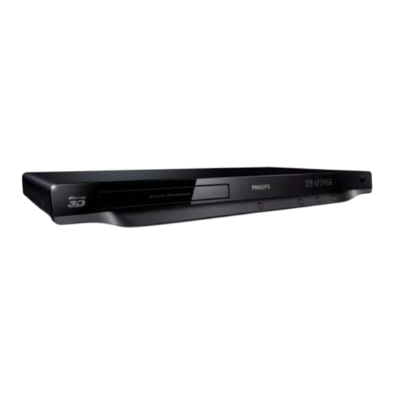
Blu-ray Disc Player
TABLE OF CONTENTS
Location of PCB Boards & version variation & repair scenario matrix..................... 1-1
Production Specifications ...............................................................................................1-2
Remote control ...............................................................................................................1-3
Brife guide ......................................................................................................................1-
Safety Instruction, Warning & Notes...............................................................................1-
Mechanical and Dismantling Instructions .......................................................................2-1
Software Version & Upgrades.........................................................................................3-1
Trouble Shooting Chart .....................................................................................................-1
Set Block & Wiring Diagrams ............................................................................5-1
Electrical Diagrams and PCB layouts ................................................................6-1
Set Mechanical Exploded view ....................................................................................... -1
Revision List ...................................................................................................................
©
Copyright 2010 Philips Consumer Electronics B.V. Eindhoven, The Netherlands
All rights reserved. No part of this publication may be reproduced, stored in a retrieval system or
transmitted, in any form or by any means, electronic, mechanical, photocopying, or otherwise without
the prior permission of Philips.
Published by Helen-RY 1125 Service Audio Printed in The Netherlands Subject to modification
Version 1.0
Version 0.0
BDP5300K/51
Page
4
9
4
7
8
-1
CLASS 1
LASER PRODUCT
©
313978535800
GB
GB
Advertisement

Related Manuals for Philips BDP5300K/51


Summary of Contents for Philips BDP5300K/51
- Page 1 LASER PRODUCT © Copyright 2010 Philips Consumer Electronics B.V. Eindhoven, The Netherlands All rights reserved. No part of this publication may be reproduced, stored in a retrieval system or transmitted, in any form or by any means, electronic, mechanical, photocopying, or otherwise without the prior permission of Philips.
- Page 2 LOCATION OF PCB BOARDS: MAIN BOARD AV BOARD POWER BOARD LOADER FV BOARD FRONT CABINET Version Variation Type/Versions BDP5300K Features Power supply rating:220-240V ,50Hz Power consumption:18W Repair Scenario Matrix Type/Versions BDP5300K Board in used Main Board Power Board AV Board Loader *Bd:Board Level Replacement *C:Component Level Repair...
- Page 3 BDP5300K/51 Product Specifications Note Region code This player can play discs with the following region codes. Blu-ray Countries Europe, United Kingdom Playable media BD-Video, BD 3D Compatibility: Hi-Speed USB (2.0) DVD-Video, DVD+R/+RW, DVD-R/-RW, Class support: USB Mass Storage Class DVD+R/-R DL (Dual Layer)
- Page 4 Remote Control During play, press the following buttons to control. Button Action Stop play. Press and hold (more than 4 seconds) to open or close the disc compartment. Pause play. Press repeatedly to slow forward frame by frame. Start or resume play. Fast backward or forward.
- Page 5 Brife Guide Register your product and get support at www.philips.com/welcome BDP5200 BDP5200 PC & Mac EN User manual VIDEO VIDEO HDMI COAXIAL COAXIA A A AL AUDIO LINE OUT UDIO LINE OU...
- Page 6 1 HDMI HDMI VIDEO COAXIAL AUDIO LINE OUT 2 VIDEO+AUDIO LINE OUT HDMI VIDEO COAXIAL AUDIO LINE OUT AUDIO LINE OUT IO LINE VIDEO VIDEO O...
- Page 7 3 COAXIAL HDMI VIDEO COAXIAL AUDIO LINE OUT COAXIAL COAXIA A L 4 AUDIO LINE OUT HDMI VIDEO COAXIAL AUDIO LINE OUT AUDIO LINE OUT...
- Page 8 SOURCE...
- Page 9 BD/BD 3D DVD/VCD/CD DivX Plus HD/MKV MP3 / JPEG...
- Page 10 Make sure that, • Use only lead-free soldering tin Philips SAC305 with order during repair, you are connected with the same potential as code 0622 149 00106. If lead-free solder paste is required, the mass of the set by a wristband with resistance.
- Page 11 1 - 10 Safety Instructions, Warnings, Notes, and Abbreviation List 2.3.5 Alternative BOM identification Abbreviation List It should be noted that on the European Service website, 0/6/12 SCART switch control signal on A/V “Alternative BOM” is referred to as “Design variant”. board.
- Page 12 Electro Magnetic Interference LORE LOcal REgression approximation EPLD Erasable Programmable Logic Device noise reduction Europe LG.Philips LCD (supplier) EXTernal (source), entering the set by Loudspeaker SCART or by cinches (jacks) LVDS Low Voltage Differential Signalling Fast BLanking: DC signal Mbps...
- Page 13 4.406250 MHz and 4.250000 MHz Sound Intermediate Frequency SMPS Switched Mode Power Supply System on Chip Sync On Green SOPS Self Oscillating Power Supply S/PDIF Sony Philips Digital InterFace SRAM Static RAM Service Reference Protocol Small Signal Board STBY STand-BY SVGA 800x600 (4:3)
- Page 14 Mechanical and Dismantling Instructions Dismantling Instruction Detailed information please refer to the model set. The following guidelines show how to dismantle the player. Step1: Remove 6 screws around the Top Cover, and then remove the Top Cover (Figure 1). Figure 1 Step2: If it is necessary to dismantle Loader or Front Panel, the Front door should be removed first.
- Page 15 Mechanical and Dismantling Instructions Detailed information please refer to the model set. Dismantling Instruction Step3: Dismantling Front Panel, disconnect the connectors (XP2, XP3,XP4)(Figure 6) Figure 3 Step4: Dismantling Front Panel, need release 2 snaps of Front Panel and 2 snaps of bottom cabinet , then gently pull the Panel out from the set.
- Page 16 Mechanical and Dismantling Instructions Dismantling Instruction Detailed information please refer to the model set. Step5: Dismantling Loader, disconnect the 3 connectors (XP5, J3, J4)(Figure 3) aiming in the below figure, and remove 4 screws that connects the loader and the bottom cabinet. (Figure 4-5) Figure 5 Step6: Dismantling Main Board and AV Board, first disconnect the connector (XP4), and then remove 5 screws.
- Page 17 C) Update software via USB Flash Drive: B) Update software via USB Flash Drive: 1) Go to www.philips.com/support to check if the latest software version is available for this player. 2) Download the software onto a USB flash drive.
- Page 18 Trouble shooting chart No display on VFD, and buttons do not work No display on VFD, and buttons do not work Check every supply voltage on main board Refer to Power supply board part normal:XP4(PIN6:5V,PIN7:12V, PIN10:-24V) Check front board Check the front board CN7’s pin signals(square-wave)VCLK,VD, VSTB, (CN1:pin10,11,12), 1,2,3 arrive the condition CN1’pin...
- Page 19 Trouble shooting chart No audio output No audio output Check if CN7\CN8 conection is ok or not pin to pin from the CN7/CN8 from AV board to mainboard board to mainboard Check whether the audio signal is right from the U15:’9pin and 10pin Check the U15 on power supply (When you play 1KHz signal disk,the (U15:11pin and 14pin=3.3V)
- Page 20 Trouble shooting chart Remote control does not work Remote control does not work Check whether the remote Replace the battery for remote control control’s battery exhausted or not. Check if the ET3045 power Check the VCC net on front board supply OK, ET3045 PIN20...
- Page 21 Trouble shooting chart Can’t read disc or can’t open the disk door Can’t read disc or can’t open the disk door Check whether the DVD loader Check the connection running is normal(the OPU is 4pin cable from the moving or eradiating the red lase) main board Check 45pin...
- Page 22 Trouble shooting chart No video display No Video display Check if CN7/CN8 fix well from Fix CN7,CN8 in AV board AV board to mainboard.(the solder of CN7/CN8 is OK ) Add L452 Check if L452 is on main BD Check R616 is Add R616 Main BD...
- Page 23 Trouble shooting chart Can not connect to network Can not connect to network Check if LFE8634(U14) Fix U14 in main board is on main board Check R580,R133,R134,R560,R Fix all the resistor 579 is on main board Change the P2 on the main board(refer to schematic of main board )
- Page 24 Trouble shooting chart Can not connect to WIFI Can not connect to WIFI Check (pin1) Check the R965 is fixed well voltage is normal(3.3V) themainboard Check the order of wifi Check the connection wire:from yellow\white\red from wifi board to to yellow \white\red is fixed or not mainboard Change the wifi wire...
- Page 25 BDP5300K/51 Block diagram: COAXIAL L+R+CVBS AV BOARD PORT HDMI SD CARD SMSC8710 Ethernet PHY AK4430 I2S OUT CVBS OUT 45PIN FCC USB signal TRAY TPC1391G4 MT8555 WIFI signal 1Gb DDR3 1333MHz LOADER: L9829A AC IN 1Gb DDR3 1333MHz OPU:SONY 470...
- Page 26 COAXIAL CVBS BDP5300K/51 Wiring diagram: AV BOARD 6 4 2 1.none 1.MUTE 2.none 2.ROUT1 3.none 3.LOUT1 4.GND 4.VCC_D 5.GND 5.GND 6.CVBS 6.SPDIF HDMI NET PORT SD CARD SMSC8701 AK4430 LOADER :L9829A I2S OUT CVBS OPU:SONY 470 1Gb DDR3 MT8555 1333M...
- Page 27 KE Board Circuit Diagram:MCU VCC3V3 VCC3V3 4.7K 4.7K MODE RST_MCU -24V_D 4PIN/2.0mm/100mm 4PIN/2.0mm/100mm +12V_D VCC3V3 R5F211B4SP R5F211B4SP M_SCL M_SDA P3_5/SSCK/SCL/CMP1_2 P3_4/SCS/SDA/CMP1_1 PCON MCU_OUT1 P3_7/CNTR0/SSO/TXD1 P3_3/TCIN/INT3/SS100/CMP1_0 POWER_KEY RESET P1_0/KI0/AN8/CMP0_0 VCC3V3 EJECT XOUT/P4_7 P1_1/KI1/AN9/CMP0_1 VCC3 VSS/AVSS P4_2/VREF XIN/P4_6 P1_2/KI2/AN10/CMP0_2 VCC3 VCC3 PLAY LED1 LED1 VCC/AVCC...
- Page 28 FE Board Circuit Diagram:VFD VFD1 VFD1 1000pF 1000pF 3DG3904M 3DG3904M 3DG3904M 3DG3904M 1000pF 1000pF 0.1uF 0.1uF 1uF/50V/Y5V 1uF/50V/Y5V 4.7K 4.7K 1uF/50V/Y5V 1uF/50V/Y5V 3DG3904M 3DG3904M 3CG3906M 3CG3906M 3DG3904M 3DG3904M -24V -24V 1000pF 1000pF SEG8 SEG7 SEG6/K6 SEG5/K5 SEG4/K4 -24V CS16312 CS16312 LED4 SEG3/K3 LED3...
- Page 29 AV Board Circuit Diagram: SPDIF ASPDIF C613 C613 R609 R609 180/1% 180/1% 0.1uF/25V/Y5V 0.1uF/25V/Y5V R610 R610 500/200mA 500/200mA C615 C615 100pF/50V/NP0 100pF/50V/NP0 100/1% 100/1% RCA/2h RCA/2h FE_GND FE_GND SPDIF OUTOUT VIDEO ASPDIF LOUT1 BUFFER IMPEDANCE AMUTE ROUT1 CON2.54-2X6 CON2.54-2X6 CVBS (Yellow) CVBS CVBSO LOUT1...
- Page 30 Power Board circuit diagram: L501 L501 680uH 680uH CY503 CY503 470PF/250Vac 470PF/250Vac C501 C501 D501 D501 D503 D503 R505A R505A R505B R505B R505C R505C R505D R505D 103/1KV 103/1KV 470PF/250Vac 470PF/250Vac CY504 CY504 R506 R506 RL207 RL207 RL207 RL207 CE501 CE501 CE502 CE502 CE503...
- Page 31 FE Board Print-layout (Top and Bottom side):...
- Page 32 FK Board Print-layout (Bottom side):...
- Page 33 AV Board Print-layout (Bottom side):...
- Page 34 Power Board Print-layout (Bottom side):...
- Page 35 Main Board Print-layout (Top side):...
- Page 36 6-10 6-10 Main Board Print-layout (Bottom side):...
- Page 37 Exploded view for BDP5300K/51:...
- Page 38 REVISION LIST Version 1.0 * Initial release for BDP5300K/51...
Need help?
Do you have a question about the BDP5300K/51 and is the answer not in the manual?
Questions and answers