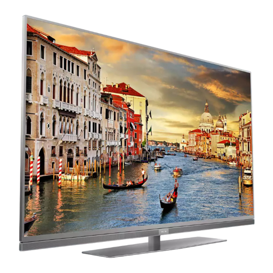
Philips 49HFL7011T/12 Service Manual

Chassis tpm16.2he la

Advertisement

Quick Links

Colour Television
Contents
11. Styling Sheets
7011 series 49"
Published by CQZ/SC 1621 Quality
©
2016
TP Vision Netherlands B.V.
All rights reserved. Specifications are subject to change without notice. Trademarks are the
property of Koninklijke Philips Electronics N.V. or their respective owners.
TP Vision Netherlands B.V. reserves the right to change products at any time without being obliged to adjust
earlier supplies accordingly.
PHILIPS and the PHILIPS' Shield Emblem are used under license from Koninklijke Philips Electronics N.V.
Page
Contents
2
2
6
10
10
10
11
27
34
43
Drawing PWB
44
48-49
50
54-55
56
83-84
85
86
87
88
89
90
93
95
96
98
99
101
102
104
105
107
108
112
113
114
115
Printed in the Netherlands
Chassis
TPM16.2HE
Page
Subject to modification
EN 3122 785 20130
LA
2016-May-27

Advertisement

Table of Contents
loading

Summary of Contents for Philips 49HFL7011T/12

  • Page 1: Table Of Contents

    Koninklijke Philips Electronics N.V. or their respective owners. TP Vision Netherlands B.V. reserves the right to change products at any time without being obliged to adjust earlier supplies accordingly. PHILIPS and the PHILIPS’ Shield Emblem are used under license from Koninklijke Philips Electronics N.V.
  • Page 2: Revision List

    Notes: software & drivers. • Figures can deviate due to the different set executions. Table 2-1 Described Model Numbers and Diversity Mechanics Schematics 49HFL7011T/12 & 4-5 & 4-7 4-10 10.1 10.3 10.4 10.5 10.8...
  • Page 3 Technical Specs, Diversity, and Connections TPM16.2HE LA EN 3 Connections Side Connectors Rear Connectors SERV .U SCART (RGB/CVBS) AUDIO IN DVI USB 3 USB 2 HDMI 4 ARC/MHL NETWORK TV ANTENNA DIGITAL HDMI 1 HDMI 2 USB1 AUDIO OUT HDMI 3 ARC 20130_001.eps Figure 2-1 Connection overview Note: The following connector colour abbreviations are used...
  • Page 4 EN 4 TPM16.2HE LA Technical Specs, Diversity, and Connections 5- HDMI ARC: Digital Video - In, Digital Audio with ARC - 8 - Cinch: Video YPbPr - In, Audio - In In/Out Gn - Video - Y / 75 W Bu - Video - Pb 0.7 V / 75 W...
  • Page 5 Technical Specs, Diversity, and Connections TPM16.2HE LA EN 5 16 - DDC_SDA DDC data - Shield 17 - Ground - D1- Data channel 18 - +5V - D0+ Data channel 19 - HPD Hot Plug Detect - Shield 20 - Ground - D0- Data channel 10 - CLK+...
  • Page 6: Precautions, Notes, And Abbreviation List

    Spare Parts the following points: • Route the wire trees correctly and fix them with the For the latest spare part overview, consult your Philips Spare mounted cable clamps. Part web portal. • Check the insulation of the Mains/AC Power lead for external damage.
  • Page 7 Precautions, Notes, and Abbreviation List TPM16.2HE LA EN 7 result in sets which have the same CTN (Commercial Type 6 = play 16 : 9 format, 12 = play 4 : 3 Number; e.g. 28PW9515/12) but which have a different B.O.M. format number.
  • Page 8 6.5 MHz. L' is Band (VESA standard for communication I, L is all bands except for Band I channel and display). Using E-DDC, LG.Philips LCD (supplier) the video source can read the EDID Loudspeaker information form the display.
  • Page 9 SOPS Self Oscillating Power Supply Serial Peripheral Interface bus; a 4-wire synchronous serial data link standard S/PDIF Sony Philips Digital InterFace SRAM Static RAM Service Reference Protocol Small Signal Board Spread Spectrum Clocking, used to reduce the effects of EMI...
  • Page 10: Mechanical Instructions

    EN 10 TPM16.2HE LA Mechanical Instructions 4. Mechanical Instructions Index of this chapter: Notes: 4.1 Cable Dressing • Figures below can deviate slightly from the actual situation, 4.2 Service Positions due to the different set executions. 4.3 Assembly/Panel Removal (for 7011T series) 4.4 Set Re-assembly Cable Dressing AmbiLight...
  • Page 11: Cable Dressing (65" 7011 Series)

    Mechanical Instructions TPM16.2HE LA EN 11 AmbiLight AmbiLight EXA02 (1062) (1061) ECN1106 CN1106 CN1190 ECN1190 LOUDSPEAKER (1185) (1053) MAIN POWER SUPPLY (1054) ECN1161 KEYBOARD CONTROL (1057) WIFI MODULE IR/LED BOARD LOUDSPEAKER LOUDSPEAKER (1056) WiFi01 (1184) (1184) 20130_101.eps Figure 4-2 Cable dressing (55" 7011 series) AmbiLight AmbiLight AmbiLight...
  • Page 12 Ensure that ESD safe measures are taken. Figure 4-5. Assembly/Panel Removal (for 7011T series) Instructions below apply to the 49HFL7011T/12, but will be similar for other 49"/55"/65" 7011T series models. 20130_103.eps Figure 4-4 Stand removal[1] back to 2016-May-27 div.table...
  • Page 13 Mechanical Instructions TPM16.2HE LA EN 13 20130_104.eps Figure 4-5 Stand removal[2] back to 2016-May-27 div.table...
  • Page 14 EN 14 TPM16.2HE LA Mechanical Instructions 4.3.2 Rear Cover 2. Unplug the connector [3] from SSB. Refer to Figure 4-7 details. 3. Lift the rear cover from the TV. Make sure that wires and Refer to Figure 4-6 Figure 4-7 for details.
  • Page 15 Mechanical Instructions TPM16.2HE LA EN 15 4.3.3 AmbiLight Panel 1. Gently release the clamps and unplug the two connectors [5] that secure the ambilight panels. Release the clips from the FFC connector that connect with the keyboard [4]. Refer to Figure 4-8 for details.
  • Page 16 EN 16 TPM16.2HE LA Mechanical Instructions 4.3.6 IR/LED Board Set Re-assembly To re-assemble the whole set, execute all processes in reverse order. Refer to Figure 4-10 for details. 1. Remove the fixation screws [1] from the stand bracket, pull out the assy from the set. Notes: 2.
  • Page 17: Service Modes, Error Codes, And Fault Finding

    Service Modes, Error Codes, and Fault Finding TPM16.2HE LA EN 17 5. Service Modes, Error Codes, and Fault Finding Index of this chapter: • X is the main version number: this is updated with a major 5.1 Service Modes change of specification (incompatible with the previous 5.2 Stepwise Start-up software version).
  • Page 18 EN 18 TPM16.2HE LA Service Modes, Error Codes, and Fault Finding Main Menu Sub-menu 1 Sub-menu 2 Description Alignments Warm R Gain To align the White Tone. See paragraph 6.3 Software Alignments in the Alignments section for a detailed description G Gain B Gain Normal...
  • Page 19 Service Modes, Error Codes, and Fault Finding TPM16.2HE LA EN 19 Default value Item Item value 49" 55" 65" Description NVM VALUE Displays the value at the NVM address of item 5 NVM STORE Press OK Use this option to save the data of item 6 to NVM address of item 5 COPY NVM to USB Press OK Use this to store the NVM data to the REPAIR folder of a FAT formatted USB memory...
  • Page 20 EN 20 TPM16.2HE LA Service Modes, Error Codes, and Fault Finding Specifications • Press the MENU/HOME button on the remote control • Ignore “Service unfriendly modes”. transmitter. • Line number for every • Press the POWER button on the remote control line (to make CSM language independent).
  • Page 21 Service Modes, Error Codes, and Fault Finding TPM16.2HE LA EN 21 Stepwise Start-up Standby Soft Mode Command Received, Switch previously in Standby Off(Mains Soft Mode (Power tact Standby Power Plug) switch) Digital Digital background background tasks started tasks completed TV Wakeup commands Received Standby...
  • Page 22 It is possible for the user to upgrade the main software via the USB port. This allows replacement of a software image in a stand alone set. A description on how to upgrade the main software can be found in the DFU or on the Philips website. 5.4.2 Introduction 19080_207_110324.eps...
  • Page 23 Service Modes, Error Codes, and Fault Finding TPM16.2HE LA EN 23 5.4.6 Content and Usage of the One-Zip Software File Example: – ERROR: 000 000 000 000 000: No errors detected – ERROR: 013 000 000 000 000: Error code 13 is the Below you find a content explanation of the One-Zip file, and last and only detected error instructions on how and when to use it.
  • Page 24 EN 24 TPM16.2HE LA Service Modes, Error Codes, and Fault Finding automatically when the error/protection is monitored by the 5.7.6 No Picture via HDMI input standby processor. In case no picture is shown and there is no LED blinking, Check if HDCP key is valid. This can be done in CSM. read the logging to detect whether “error devices”...
  • Page 25 Picture mode Screen size Green Blue signal strength of at least 1 mV and a frequency of Normal (9000K) 49HFL7011T/12 127 61.25 MHz (channel 3). 55HFL7011T/12 125 • LATAM models: an NTSC M TV-signal with a signal 65HFL7011T/12 119 strength of at least 1 mV and a frequency of...
  • Page 26 For example, a cable from the Table 6-3 Display code overview PSU connector CN902 to the SSB connector CN701, will have the position number ECN902. CTN_ALT BOM# Panel Type Display Code 49HFL7011T/12 TPT490U2-EQLSHA.G SC2D 55HFL7011T/12 TPT550U2-EQLSHA.G S1F 65HFL7011T/12 TPT650UA-QVN04.U S400 Reset of Repaired SSB...
  • Page 27: Circuit Descriptions

    Circuit Descriptions TPM16.2HE LA EN 27 7. Circuit Descriptions Index of this chapter: Introduction 7.1 Introduction The TPM16.2HE LA is a new chassis launched in Europe in 7.2 Power Supply 2016. The whole range is covered by MT5593U. 7.3 DC/DC Converters The major deltas versus its predecessor support DVB-C;...
  • Page 28 EN 28 TPM16.2HE LA Circuit Descriptions 7.1.3 SSB Cell Layout DC/DC COMMON INTERFACE MT5593U SCART HDMI TUNER NETWORK Digital Audio HDMI Headphone 20130_200.eps Figure 7-1 SSB layout cells (top view) back to 2016-May-27 div.table...
  • Page 29 7.2.2 Diversity specifications! This part is available in the regular market. Consult the Philips Service web portal for the order codes of the The diversity in power supply units is mainly determined by the boards. diversity in displays.
  • Page 30 EN 30 TPM16.2HE LA Circuit Descriptions Connector Number CN9101 CN8602 CN9101 CN8603 CN9101 CN8603 Description to SSB to panel to SSB to panel to SSB to panel PS_ON n.c. PS_ON VLED- PS_ON VLED- PS_ON n.c. 3D_ON VLED- VLED- VLED- VLED- VLED- VLED- n.c.
  • Page 31 Circuit Descriptions TPM16.2HE LA EN 31 7.3.1 Power layout SSB U4304Pin5, +3V3-Standby U4405,AMBI-Power L4101,+2V5-NT L4400,+5V-SW L4301,+1V5-DDR L4302, +1V0VCCK L4102,+1V0-BST C5200, +12V-Audio2 U4303, Pin6, +1V8EMMC C5100, +12V-Audio1 L4103, +1V2 20130_202.eps Figure 7-4 Power SSB Top View back to 2016-May-27 div.table...
  • Page 32 EN 32 TPM16.2HE LA Circuit Descriptions Q4101,+3V3-NT Q4104,+1V5-NT Q3304,Pin8,12V U4300,Pin6+1V0-AVDD 20130_203.eps Figure 7-5 Power SSB Bottom View Front-End Analogue and DVB-T/T2, DVB-C reception DTST243IH133T 7.4.1 Front-End Analogue and DVB C reception The Front-End for analogue tuner consist of the following key components: IF_AGC IF_AGC...
  • Page 33 Circuit Descriptions TPM16.2HE LA EN 33 7.4.2 DTV T2 reception Video and Audio Processing - MT5593UGIJ The MT5593UGIJ is the main audio and video processor (or System-on-Chip) for this platform. It has the following features: The Front-End for DVT part consist of the following key components: •...
  • Page 34: Ic Data Sheets

    EN 34 TPM16.2HE LA IC Data Sheets 8. IC Data Sheets This chapter shows the internal block diagrams and pin configurations of ICs that are drawn as “black boxes” in the electrical diagrams (with the exception of “memory” and “logic” ICs).
  • Page 35 IC Data Sheets TPM16.2HE LA EN 35 Pinning Information MT5593UGIJ SPI_DAT CI_TSV DEMOD USB_DP USB_DP HDMI_0 HDMI_0 HDMI_0 HDMI_0 HDMI_1 HDMI_1 HDMI_2 HDMI_3 AVDD10 AVDD10 SSUSB_ AVDD33 SSUSB_ SSUSB_ NC_A1 CI_A5 CI_A6 CI_A7 CI_A12 CI_MDI1 CI_MDI0 CI_INT AIN_R3 AIN_R1 NC_A38 _TSCLK _RX_2 _RX_1...
  • Page 36 EN 36 TPM16.2HE LA IC Data Sheets Diagram 10-3-5 FE-TUNER-DEMOD-TPV, B05, NT72324BG-35 (IC U3100) Block diagram NT72324BG DDR3 PHY Leon 16-Lane 6-Port Vx1 TX/ PreCM SR-EX LVDS RX / Mute White Local Gamma Dither Detect Balance Dimming 12-Lane Vx1 RX 20030_304.eps Figure 8-3 Internal block diagram and pin configuration back to...
  • Page 37 IC Data Sheets TPM16.2HE LA EN 37 Diagram 10-3-15 DCDC-SYSTEM-POWER2, B15, AOZ1360DIL (IC U4405) Block diagram AOZI360DIL 1µF 1µF Gate Driver & 5V Linear Current Limit Slew Rate Regulator Control 84.5kΩ 5.5V UVLO Comparator Thermal Shutdown AOZ1360 Pinning information 20030_303.eps Figure 8-4 Internal block diagram and pin configuration back to 2016-May-27...
  • Page 38 EN 38 TPM16.2HE LA IC Data Sheets Diagram 10-3-15 DCDC-SYSTEM-POWER2, B15, G5318RE1D (IC U4401) Block diagram G5318RE1D On-Time On-Time PGOOD PGOOD Off-Time Off-Time DISCHG DISCHG controller controller 0.7V 0.7V Reference Reference SKIP/force PWM SKIP/force PWM Freq Freq Setting Setting TRIP TRIP Pinning information PGOOD...
  • Page 39 IC Data Sheets TPM16.2HE LA EN 39 Diagram 10-3-14 DCDC-SYSTEM-POWER1, B14, RT8079GQW (IC U4302) Block diagram RT8079GQW Internal pull up Over Temperature current Protection UVLO Enable Comparator Shutdown Current EN Threshold Control Sense BOOT RT/SYNC Oscillator Control Driver Slope Logic Compensation Comparator SS/TR...
  • Page 40 EN 40 TPM16.2HE LA IC Data Sheets Diagram 10-3-16 AUDIO-1st-CLASS-D-AMP, B16, TAS5760LDDCAR (IC U5100) Block diagram TAS5760LDDCAR PVDD GVDD_REG Internal Internal Reference Internal Gate DRVDD Voltage Regulators Drive Regulator Supplies Closed Loop Class D Amplifier SFT_CLIP Full Bridge Digital to SPK_OUTA+ Digital Power Stage...
  • Page 41 IC Data Sheets TPM16.2HE LA EN 41 Diagram 10-3-5 FE-TUNER-DEMOD-TPV, B01, Si21692-C50 (IC U2102) Block diagram Si21692-C50 1.2, 3.3V RESETB MP_A_A Si21692C MP_C_A S_ADC_IP_A ADC_A S_ADC_IN_A TS1_SYNC S_ADC_QP_A Dual Satellite TS1_DATA S_ADC_QN_A ADC_A DEMODULATOR_A CORE Tuner TS1_VAL TC_ADC_P_A TS_A TS1_CLK ADC_A TC_ADC_N_A DiSEqC_OUT_A...
  • Page 42 EN 42 TPM16.2HE LA IC Data Sheets Diagram 10-3-15 DCDC-SYSTEM-POWER2, B15, RT8079GQW (IC U4403) Block diagram LNBH26LSPQR DSQIN-A ADDR DSQIN-B LX-A LX-B I²C Digital core Drop control PGND PGND Tone ctrl Diagnostics VUP-B VUP-A Protections Current Linear Linear Limit VOUT-A VOUT-B Regulator Regulator...
  • Page 43: Block Diagrams

    Block Diagrams TPM16.2HE LA EN 43 9. Block Diagrams Block diagram series EU/RU T UHD100 2x DDR3 2x DDR3 1x DDR3 eMMC 1833 1833 1833 EU#1 EU#3 EU#6 PQ BO 16GB 4Gbit 4Gbit 4Gbit HTV RJ50 Wi-Fi 11AC Connector 3x DDR3 1x DDR3 HTV 12V 1600...
  • Page 44: Circuit Diagrams And Pwb Layouts

    Circuit Diagrams and PWB Layouts TPM16.2HE LA EN 44 10. Circuit Diagrams and PWB Layouts 10.1 A 715G7720 PSU 10-1-1 AC input AC input F9901 FB9901 NR9903 BEAD SG9901 FB9905 FB9906 BEAD R9901 510k 1/2W C9911 C9913 220PF 250V BD9901 CN9901 GBJ1008-FUC Vsin...
  • Page 45 Circuit Diagrams and PWB Layouts TPM16.2HE LA EN 45 10-1-2 PFC LD7591T PFC LD7591T BD9801 KBP208G-C C9801 47PF FB9805 D9802 FMNS-1106S L9802 Vsin Vbus BEAD 120uH L9801 C9802 C9819 200uH C9806 10NF 1KV 1UF 450V 1UF 450V C9804 C9803 Q9801 82uF 450V 82uF 450V IPA60R125P6...
  • Page 46 Circuit Diagrams and PWB Layouts TPM16.2HE LA EN 46 10-1-3 Main power SSC3S121A Main power SSC3S121A Vbus T9101 12VS POWER X'FMR Q9104 L9101 C9113 470uF 25V 1.1uH PZ0703ETF +12V R9141 Vbus R9142 100KOHM +-5% 1/8W R9140 D9116 39R 5% SR810-05 D9101 C9120 SARS02...
  • Page 47 Circuit Diagrams and PWB Layouts TPM16.2HE LA EN 47 10-1-4 LED DRIVER SSC9522S LED Driver SSC9522S VLED1 D8104 FMX-23S R8101 0.1R L8101 HS8101 Vbus HEAT SINK +VLED C8101 FB_LLC D8109 R8118 R8175 R8176 R8177 R8178 R8179 +VCC2 D8101 R8109 D8102 R8110 UF4007 10ohm +/-1% 1/8W...
  • Page 48 Circuit Diagrams and PWB Layouts TPM16.2HE LA EN 48 10-1-5 Power layout top U9102 C9820 C9103 FB9803 HS9102 HS9103 HS9101 HS9801 C9803 C9804 Q9111 Q9104 D9802 Q9101 Q9801 L9801 J9856 C9818 D9106 L9101 J9811 C9145 C9801 R9101 J9860 J9818 D9101 D9116 J9859 C9116...
  • Page 49 Circuit Diagrams and PWB Layouts TPM16.2HE LA EN 49 10-1-6 Power layout bottom R9115 R9128 R9156 R9164 C9121 R9121 R9104 R9124 R9129 R9819 C9104 R9801 RJ9801 R9118 R9817 R9108 R9119 R9802 R9815 RJ9804 C9141 R9812 Q9109 R9143 RJ9805 R9157 RJ9813 R9811 R9814 C9119...
  • Page 50: A 715G7831 Psu

    Circuit Diagrams and PWB Layouts TPM16.2HE LA EN 50 10.2 A 715G7831 PSU 10-2-1 AC input AC input HS9901 HEAT SINK BR_IN FB9901 F9901 BEAD C9913 NR9901 220PF 250V NR9903 1.5R SG9901 C9911 T6.3AH 250V 22PF 250V L9903 NR9902 BD9901 SW9901 CN9902 R9299...
  • Page 51 Circuit Diagrams and PWB Layouts TPM16.2HE LA EN 51 10-2-2 PFC with LD7591T PFC with LD7591T D9801 D9802 C9801 47PF HS9801 IN5408G-04 IN5408G-04 HEAT SINK Vbus D9803 FMNS-1106S L9801 FB9801 FB9804 FB9803 127R 170uH NC_BEAD BEAD R9821 Vsin C9802 C9803 C9804 C9805 NC_2Mohm 1/4W +/-1%...
  • Page 52 Circuit Diagrams and PWB Layouts TPM16.2HE LA EN 52 10-2-3 Flyback with SSC3S121 Flyback with SSC3S121 L9101 R9136 R9137 R9138 NC_1.1uH BR_IN BR_out 620K 1/4W 620K 1/4W 620K 1/4W HS9102 T9101 D9107 Q9104 L9102 POWER X'FMR NC_SR810-05 PZ0703ETF 1.1uH Vbus +12V 12VS D9100...
  • Page 53 Circuit Diagrams and PWB Layouts TPM16.2HE LA EN 53 10-2-4 LLC with TPV101 LLC with TPV101 FB8601 HS8601 D8602 Vbus BEAD T8601 R8601 1.5M 1% 1/4W C8601 VLED 10NF 1KV FB8602 R8602 1.5M 1% 1/4W HEAT SINK BEAD D8601 R8603 D8605 R8604 R8605...
  • Page 54 Circuit Diagrams and PWB Layouts TPM16.2HE LA EN 54 10-2-5 Power layout top C9916 FB9916 D9100 J950 J949 FB9917 C9123 D9107 L9801 C9117 DRA2 Q9111 T9101 Q9801 R9808 HS9102 HS9801 C9116 L9102 R9809 D9109 R9800 C9817 C9806 L9101 C9145 FB9803 C9109 D9101 C9149...
  • Page 55 Circuit Diagrams and PWB Layouts TPM16.2HE LA EN 55 10-2-6 Power layout bottom TEST3 D9106 R9114 R9127 D9104 R9801 C9124 C9133 R9815 R9803 D9804 C9134 R9126 D9805 Q9803 D9105 C9135 C9807 U9111 R9812 C9136 R9807 C9811 D9806 R9813 U9801 C9812 C9816 C9810 C9815...
  • Page 56: B 715G8000 Ssb

    Circuit Diagrams and PWB Layouts TPM16.2HE LA EN 56 10.3 B 715G8000 SSB 10-3-1 SOC-EMMC SOC-EMMC 24MHz CRYSTAL MT5593 HEAT SINK +3V3-STANDBY +3V3-STANDBY CN9400 D9402 D9403 X9400 HEAT SINK R9486 LBAV99WT1G LBAV99WT1G XTALI XTALO NC/0R05 OHM 24MHz C9401 C9400 R9400 R9401 DEBUG 10PF 50V...
  • Page 57 Circuit Diagrams and PWB Layouts TPM16.2HE LA EN 57 10-3-2 SOC-DDR3-1-2 SOC-DDR3-1-2 U9400-1 M0-MA0 M0-DQM0 ARA0 ARDQM0 M0-MA1 M0-DQS0p ARA1 ARDQS0 TP9115 TP9116 M0-MA2 M0-DQS0n +1V5-DDR +1V5-DDR ARA2 ARDQS0# M0-MA3 M0-MD0 ARA3 ARDQ0 M0-MA4 M0-MD1 ARA4 ARDQ1 M0-MA5 M0-MD2 ARA5 ARDQ2 M0-MA6 M0-MD3...
  • Page 58 Circuit Diagrams and PWB Layouts TPM16.2HE LA EN 58 10-3-3 SOC-DDR3-3-4 SOC-DDR3-3-4 U9400-2 TP9211 TP9212 AR12 M1-MA0 M1-DQM0 +1V5-DDR +1V5-DDR BRA0 BRDQM0 M1-MA1 AP15 M1-DQS0p AN14 BRA1 BRDQS0 M1-MA2 M1-DQS0n BRA2 BRDQS0# M1-MA3 AP13 M1-MD0 AR15 BRA3 BRDQ0 AT10 M1-MA4 M1-MD1 BRA4 BRDQ1...
  • Page 59 Circuit Diagrams and PWB Layouts TPM16.2HE LA EN 59 10-3-4 SOC-DDR3-5 SOC-DDR3-5 U9400-13 M2-MA0 M2-DQM0 TP9346 CRA0 CRDQM0 M2-MA1 M2-DQS0p +1V5-DDR CRA1 CRDQS0 M2-MA2 M2-DQS0n CRA2 CRDQS0# M2-MA3 M2-MD0 CRA3 CRDQ0 M2-MA4 M2-MD1 CRA4 CRDQ1 M2-MA5 M2-MD2 CRA5 CRDQ2 M2-MA6 M2-MD3 CRA6 CRDQ3...
  • Page 60 Circuit Diagrams and PWB Layouts TPM16.2HE LA EN 60 10-3-5 FE-TUNER-DEMOD-TPV Audio/Video IO/SPDIF FE-TUNER-DEMOD-TPV TU2100 U2104 FB2100 30R AZ1117CH-3.3TRG1 T P2164 T P2165 +3V3-TUNER-ANA C2181 +5V-SW +3V3-DVB A3.3V +3V3-DEMOD +3V3-DEMOD VOUT 100N16V C2172 C2176 +1V8-TUNER 1.8V SCL-T1 NC/22pF 50V NC/22pF 50V T P2130 T P2132 SDA-T1...
  • Page 61 Circuit Diagrams and PWB Layouts TPM16.2HE LA EN 61 10-3-6 BE-NT324a-Vx1-INPUT BE-NT324a-Vx1-INPUT SPLASH-ON SPLASH-ON MT5593 Vx1 / LVDS OUTPUT NT324 Vx1 INPUT SOC-BL-ONn SOC-BL-ONn +3V3 +3V3-NT SCL-DISP SCL-DISP SDA-DISP SDA-DISP SCL-BE SCL-BE SDA-BE SDA-BE MT5593UGIJ U9400-3 AV25 NT-AMBI-SPI-SWITCH BE0P NT-AMBI-SPI-SWITCH 8 AU25 NT-AMBI-SPI-CLK BE0N...
  • Page 62 Circuit Diagrams and PWB Layouts TPM16.2HE LA EN 62 10-3-7 BE-NT324b-GPIO BE-NT324b-GPIO SPLASH-ON SPLASH-ON BL-I-CTRLn NT324 CONTROL BL-I-CTRLn 15,20 NT-BL-ONn NT-BL-ONn BL-DIM1 BL-DIM1 9,15 BL-DIM1n BL-DIM1n BL-DIM2 BL-DIM2 BL-DIM3 BL-DIM3 +3V3-NT BL-DIM4 BL-DIM4 BL-DIM5 BL-DIM5 BL-DIM6 BL-DIM6 BL-DIM7 BL-DIM7 BL-DIM8 +3V3-DISP BL-DIM8 NT72324BG-35...
  • Page 63 Circuit Diagrams and PWB Layouts TPM16.2HE LA EN 63 10-3-8 BE-NT324c-TX-VB1 BE-NT324c-TX-VB1 SPLASH-ON SPLASH-ON BL-I-CTRLn NT324 CONTROL BL-I-CTRLn 15,20 NT-BL-ONn NT-BL-ONn BL-DIM1 BL-DIM1 9,15 BL-DIM1n BL-DIM1n BL-DIM2 BL-DIM2 BL-DIM3 BL-DIM3 +3V3-NT BL-DIM4 BL-DIM4 BL-DIM5 BL-DIM5 BL-DIM6 BL-DIM6 BL-DIM7 BL-DIM7 BL-DIM8 +3V3-DISP BL-DIM8 NT72324BG-35...
  • Page 64 Circuit Diagrams and PWB Layouts TPM16.2HE LA EN 64 10-3-9 BE-NT324d-POWER BE-NT324d-POWER NT324 POWER +1V1-NT NT72324BG-35 U3100H +3V3-NT-IO AE15 AE26 VDD11V_1 IO33V_1 AE16 AE27 VDD11V_2 IO33V_2 AE17 AF26 NT72324BG-35 AE18 VDD11V_3 IO33V_3 AF27 U3100I AE19 VDD11V_4 IO33V_4 AE20 VDD11V_5 AF14 VDD11V_6 VDD11V_7 AF15...
  • Page 65 Circuit Diagrams and PWB Layouts TPM16.2HE LA EN 65 10-3-10 BE-NT324e-DDR BE-NT324e-DDR NT324 DDR A-B NT72324BG-35 U3501 U3502 U3100A TP3671 NT-A-DQL0 NT-M-A0 TP3616 NT-B-DQL0 NT-M-A0 DQL0 DQL0 NT-M-A0 NT-A-DML NT-A-DQL1 NT-M-A1 NT-B-DQL1 NT-M-A1 TP3672 TP3617 MADD0 ADML_DM2 DQL1 DQL1 NT-M-A1 NT-A-DMU TP3673 NT-A-DQL2...
  • Page 66 Circuit Diagrams and PWB Layouts TPM16.2HE LA EN 66 10-3-11 BE-NT324f-DDR BE-NT324f-DDR NT324 DDR C-D U3601 U3602 TP3754 NT-C-DQL0 NT-S-A0 TP3839 NT-D-DQL0 NT-S-A0 DQL0 DQL0 NT-C-DQL1 NT-S-A1 NT-D-DQL1 NT-S-A1 NT72324BG-35 TP3739 TP3840 DQL1 DQL1 NT-C-DQL2 NT-S-A2 NT-D-DQL2 NT-S-A2 U3100B TP3740 TP3841 DQL2 DQL2...
  • Page 67 Circuit Diagrams and PWB Layouts TPM16.2HE LA EN 67 10-3-12 DCDC-Novatek-POWER DCDC-Novatek-POWER +12V +12V TP4130 +3V3 Q4100 FB4100 30R 1A TP4107 LMUN5313DW1T1G Q4101 AO3416 R4100 R4103 NC/1 OHM 5% 1/16W R4102 TP4128 10K+-5%1/16W TP4127 +3V3-NT NC/1 OHM 5% 1/16W TP4103 TP4108 C4117 ZD4101...
  • Page 68 Circuit Diagrams and PWB Layouts TPM16.2HE LA EN 68 10-3-13 DCDC-SOC-VCCK-DVSS DCDC-SOC-VCCK-DVSS U9400-11 +1V0-VCCK +1V0-VCCK AA15 DVSS DVSS AA16 U9400-12 DVSS DVSS AA17 DVSS DVSS AA18 AC25 AA25 DVSS DVSS VCCK VCCK AA19 AC26 AA26 DVSS DVSS VCCK VCCK AA20 AC27 AA27 DVSS...
  • Page 69 Circuit Diagrams and PWB Layouts TPM16.2HE LA EN 69 10-3-14 DCDC-SYSTEM-POWER1 DCDC-SYSTEM-POWER1 12V-DETECT 12V-DETECT 17,20 BL-I-CTRLn BL-I-CTRLn 8,20 SOC-BL-ONn SOC-BL-ONn +3V5-SB D4304 +3V3-STANDBY NT-BL-ONn NT-BL-ONn NC/FB340M TP4326 NT-LCD-PWR-ON DC POWER INPUT +12V FB4307 120R/3000mA +12V-AUDIO NT-LCD-PWR-ON 8,9,18 BL-DIM1 BL-DIM1 CN1190 D4303 R4104 BL-DIM2...
  • Page 70 Circuit Diagrams and PWB Layouts TPM16.2HE LA EN 70 10-3-15 DCDC-SYSTEM-POWER2 DCDC-SYSTEM-POWER2 LNBOUT-A LNBOUT-A 6 LNBOUT-B LNBOUT-B 6 FB4400 +12V TP4409 F22-DISEQC-TX1 F22-DISEQC-TX1 6 F22-DISEQC-TX2 F22-DISEQC-TX2 6 +3V5-SB 30R 1A LNB1 LNB1 R4441 TP4439 LNB2 LNB2 SDA-FE NC/4.7K 1/16W SDA-FE 6,25 SCL-FE SCL-FE...
  • Page 71 Circuit Diagrams and PWB Layouts TPM16.2HE LA EN 71 10-3-16 AUDIO-1st-CLASS-D-AMP AUDIO-1st-CLASS-D-AMP 12V-DETECT 15,20 12V-DETECT AUDIO-RESETn 18,20,28 AUDIO-RESETn SPEAKER CONNECTOR +12V-AUDIO +12V-AUDIO1 AUDIO-HP-R +3V3-AUDIO1 +3V3 +12V-AUDIO1 AUDIO-HP-R AUDIO-HP-L AUDIO-HP-L All speaker connectors use same footprint R5100 R5101 SOC-I2S-MCLK 0R05 OHM 18,25,27 SOC-I2S-MCLK SOC-I2S-BCLK...
  • Page 72 Circuit Diagrams and PWB Layouts TPM16.2HE LA EN 72 10-3-17 AUDIO-2nd-CLASS-D-AMP AUDIO-2nd-CLASS-D-AMP SOC-TX-BO SOC-TX-BO NT-LCD-PWR-ON 8,9,15 NT-LCD-PWR-ON SOC-RX-BO SOC-RX-BO +3V3-AUDIO2 +3V3 +12V-AUDIO2 +12V-AUDIO AUDIO-RESETn 17,20,28 AUDIO-RESETn +12V-AUDIO2 SOC-I2S-MCLK NT-CTRL-DISP1 R5200 R5201 17,25,27 SOC-I2S-MCLK NT-CTRL-DISP1 8,9 SOC-I2S-BCLK NT-CTRL-DISP3 17,25,27 SOC-I2S-BCLK NT-CTRL-DISP3 8,9 0R05 OHM SOC-I2S-LRCK NT-CTRL-DISP6...
  • Page 73 Circuit Diagrams and PWB Layouts TPM16.2HE LA EN 73 10-3-18 PCMCIA PCMCIA U6100B CA-A-MOCLK CA-A-MICLK MOCLKA MICLKA CA-A-MOSTRT CA-A-MISTRT MOSTRTA MISTRTA C6200 CA-A-MOVAL CA-A-MIVAL C6203 MOVALA MIVALA CA-A-MDO0 CA-A-MDI0 NC/10PF 50V NC/10PF 50V MDOA0 MDIA0 CA-A-MDO1 CA-A-MDI1 MDOA1 MDIA1 CA-A-MDO2 CA-A-MDI2 MDOA2 MDIA2...
  • Page 74 Circuit Diagrams and PWB Layouts TPM16.2HE LA EN 74 10-3-19 CIMAX CIMAX CA-A-PWR-EN CA-A-PWR-EN 19 CA-A-OCB CA-A-OCB 19 CA-B-PWR-EN CA-B-PWR-EN 19 CA-B-OCB CA-B-OCB 19 R6187 680R 1/16W 5% +3V3-CIMAX U6100A 10PF 50V C6100 +3V3-CIMAX TS-CD1-CLK TS-CD1-CLK 6 TP6128 TS-IPTV-CLK R6100 47 OHM 1/16W TS-OUT1-CLK R6106...
  • Page 75 Circuit Diagrams and PWB Layouts TPM16.2HE LA EN 75 10-3-20 HDMI-INPUTS HDMI-INPUTS HDMI4 Connected to SiI9777 RX port 0 HDMI3 Connected to SiI9777 RX port 1 CD-SENSE CD-SENSE R7144 +5V-SW D7105 HDMI0-5V 0R05 OHM MHL-SENSE LBAT54CWT1G TP7325 CD-SENSE C7111 TP7323 CN1308 TP7315 100N16V...
  • Page 76 Circuit Diagrams and PWB Layouts TPM16.2HE LA EN 76 10-3-21 HDMI-SOC-ARC HDMI-SOC-ARC R7200 100OHM1/16W U9400-6 Analog Power HDMI-CEC-IN HDMI-CEC-IN HDMI_CEC HDMI_0_RX_0 HDMIBST-TX2-TX0P 24 HDMI_0_RX_0B HDMIBST-TX2-TX0N 24 HDMIBST-TX2-SCL HDMI-MUX-IRQn HDMIBST-TX2-SCL HDMIBST-TX2-TX1P 24 HDMI-MUX-IRQn 24 HDMI_0_SCL HDMI_0_RX_1 HDMIBST-TX1-SCL +3V3-AVDD +1V0-AVDD HDMIBST-TX1-SCL HDMIBST-TX2-TX1N 24 HDMI_1_SCL HDMI_0_RX_1B HDMI2-SOC-SCL...
  • Page 77 Circuit Diagrams and PWB Layouts TPM16.2HE LA EN 77 10-3-22 HDMI_Sil9777_BOSTON-POWER HDMI-SiI9777-BOSTON-POWER +3V3 +5V-SW FB7300 120R TP7300 Q7300 XTAL-VDD33 +3V3 TP7301 AO3414 R7301 C7300 C7301 1K 1/16W R7300 VDD33OUT 100N16V 10UF 6.3V X5R +-20% VDD33OUT C7366 NC/10000pF 50V 0R05 OHM C7302 C7303 SBVCC5V...
  • Page 78 Circuit Diagrams and PWB Layouts TPM16.2HE LA EN 78 10-3-23 HDMI-Sil9777 BOSTON-BRIDGE HDMI-SiI9777 BOSTON-BRIDGE +3V3 VDD33OUT +3V3 HDM I BOSTON RESET R7448 R7400 R7401 10K+-5%1/16W 470 OHM 1/16W NC/10K+-5%1/16W +3V3 HDMI-MUX-RESETn HDMI-BST-RSTn R7402 C7409 NC/4.7K 1/16W HDMI-BST-RSTn R7403 NC/0R05 OHM 100N16V LED7400 +5V-SW...
  • Page 79 Circuit Diagrams and PWB Layouts TPM16.2HE LA EN 79 10-3-24 SCART-YPbPr-CVBS SCART-YPbPr-CVBS AGC-ANA-SOC AGC-ANA-SOC SOC-I2S-SD0 17,18,27 SOC-I2S-SD0 NC/4.7K 1/16W SPDIF-OUT CN1309 SPDIF-OUT SOC-I2S-SD1 C7501 18,27 SOC-I2S-SD1 S7500 NC/10000pF 50V R7500 NC/470PF 50V SOC-I2S-SD2 18,27 SOC-I2S-SD2 C7500 SPG_0001-0015 TER-IFp-SOC C7502 TER-IFp-SOC 6 TP7524 1UF16V R7501...
  • Page 80 Circuit Diagrams and PWB Layouts TPM16.2HE LA EN 80 10-3-25 CTRL-CONNECTORS CTRL-CONNECTORS AMBI-SPI-CLK AMBI-SPI-CLK 8 AMBI-SPI-MOSI AMBI-SPI-MOSI 8 AMBI-TEMP AL+KEY AMBI-TEMP 20 +3V3-STANDBY SCL-AMBI SCL-AMBI SDA-AMBI SDA-AMBI R8401 SOC-CTRL-DISP1 6.8K 1/16W SOC-CTRL-DISP1 7 R8420 10OHM R8402 10OHM KEY BOARD KEY BOARD KEY BOARD RC-IR RC-IR...
  • Page 81 Circuit Diagrams and PWB Layouts TPM16.2HE LA EN 81 10-3-26 CTRL-ETHERNET-PHY CTRL-ETHERNET-PHY U9400-10 LAN-PWR-EN LAN-PWR-EN 20 ETHERNET-TXp ETHERNET PHY TXVP_0 ETHERNET-TXn WIFI-IRQn TXVN_0 WIFI-IRQn 20 BT-IRQn CN1313 +3V3-USB Power BT-IRQn 20 Y 37 ETHERNET-RXp RXVP_1 Y 38 ETHERNET-RXn RJ45 RJ45 CONN RXVN_1 TP8204 USB-RESETn...
  • Page 82 Circuit Diagrams and PWB Layouts TPM16.2HE LA EN 82 10-3-27 RC-HTV RC-HTV RC-IR RC-IR 2,18,26 SOC-RX-SERVICE SOC-RX-SERVICE 2 SOC-TX-SERVICE SOC-TX-SERVICE 2 AUDIO-RESETn AUDIO-RESETn 17,18,20 AUDIO-HTV-L AUDIO-HTV-L 25 AUDIO-HTV-R AUDIO-HTV-R 25 AUDIO-PD1n AUDIO-PD1n Bathroom SPK IR IN/OUT +3V3-STANDBY +3V3-STANDBY +3V3-STANDBY +3V3-STANDBY +3V3-STANDBY R5482 R5495...
  • Page 83 Circuit Diagrams and PWB Layouts TPM16.2HE LA EN 83 10-3-28 SSB layout top CN1112 CN1106 CN1113 C4342 R4430 ZD5419 C4324 CN1107 C4456 C5453 C5459 C5456 R4331 R4428 U4405 CN1111 SEN2 CN1190 C4384 FB5415 C5463 FB5416 CN1318 C4325 R5488 R8420 C4458 R8430 R4335 C8407 C8408 C8409...
  • Page 84 Circuit Diagrams and PWB Layouts TPM16.2HE LA EN 84 10-3-29 SSB layout bottom C5436 R5459 R5458 FB4301 C5441 R8428 R5460 R5457 FB4300 R8427 R8438 C5438 U5404 C8415 R5455 R8431 C8416 R5454 R8432 R3235 C5437 C5435 R3241 R5473 R5475 D4303 C4108 D4304 Q5412 R4440...
  • Page 85: J 715G7788 Ir/Led Panel

    Circuit Diagrams and PWB Layouts TPM16.2HE LA EN 85 10.4 J 715G7788 IR/LED Panel 10-4-1 LED&IR&3D&Light sensor LED&IR&3D&Light sensor L i g h t S e n s o r CN201 LED_R DVD3V3 DVD3V3 C222 1uF 10V R 2 2 4 R 2 2 3 I 2 C a d d r...
  • Page 86 Circuit Diagrams and PWB Layouts TPM16.2HE LA EN 86 10-4-2 IR/LED board layout Layout IR/LED panel (top side) LED201 LED213 LED211 U221 LED214 LED212 U211 Q201 R211 Layout IR/LED panel (bottom side) U212 CN201 2015-08-28 IR/LED panel 715G7788 layout top/bottom 20030_541.eps back to 2016-May-27...
  • Page 87: E 715G7872 Keyboard Control Panel

    Circuit Diagrams and PWB Layouts TPM16.2HE LA EN 87 10.5 E 715G7872 Keyboard control panel 10-5-1 C O N N S S B JOYST ICK D i r e c t i o n Vo l ta g e s w i t c h Key f unction Resistance 2 - 5...
  • Page 88 Circuit Diagrams and PWB Layouts TPM16.2HE LA EN 88 10-5-2 Key board layout Layout Keyboard control panel (top side) SW26 Layout Keyboard control panel (bottom side) SW01 SW11 2015-06-06 Keyboard control panel 715G7872 layout top/bottom 20030_539.eps back to 2016-May-27 div.table...
  • Page 89: E 715G7065 Keyboard Control Panel

    Circuit Diagrams and PWB Layouts TPM16.2HE LA EN 89 10.6 E 715G7065 Keyboard control panel 10-6-1 Key+AL KEY+AL CONN TO SSB JOYSTICK Direction switch Key functionResistance Voltage Center 2-5 short Menu CN01 CN01 CN04 CN04 Right 1-5 short 0.5V KEY1 AMBI_SPI_CLK Left 4-5 short...
  • Page 90 Circuit Diagrams and PWB Layouts TPM16.2HE LA EN 90 10-6-2 Key board layout Layout Keyboard control panel (top side) CN04 CN01 Layout Keyboard control panel (bottom side) SW01 2014-11-06 Keyboard control panel 715G7065 layout top/bottom 19812_518.eps back to 2016-May-27 div.table...
  • Page 91 Circuit Diagrams and PWB Layouts TPM16.2HE LA EN 91 10.7 ALC 715G7789 LED board 10-7-1 LOGO LOGO L i g h t i n g L O G O 3V3SB 3V3SB CN301 LOGO 3V3SB CONN R301 R302 2R2 1/16W 5% 2R2 1/16W 5% R303 LOGO...
  • Page 92 Circuit Diagrams and PWB Layouts TPM16.2HE LA EN 92 10-7-2 LED board layout top/bottom Layout LED board (top side) Layout LED board (bottom side) CN16 CN17 CN301 2015-07-01 LED board 715G7789 layout top/bottom 20030 543.eps back to 2016-May-27 div.table...
  • Page 93: Al 715G6981 Ambilight Board

    Circuit Diagrams and PWB Layouts TPM16.2HE LA EN 93 10.8 AL 715G6981 Ambilight Board 10-8-1 TCL5971 AL01 AL01 TCL5971 +12V +12V XA02 XA02 XA05 XA05 CONN CONN NC/CONN +3V3 C003 C003 100N16V 100N16V R012 R012 27K 1/16W 5% 27K 1/16W 5% R008 R008 10K 1%...
  • Page 94 Circuit Diagrams and PWB Layouts TPM16.2HE LA EN 94 10-8-2 Ambilight 8-LED AL02 AL02 Ambilight 8-LED +12V R017 R017 D006 D006 D007 D007 D008 D008 PWM2-B1 R018 R018 560R 560R PWM2-R1 PWM2-G1 C012 C012 C013 C013 100NF 25V 100NF 25V NC/100NF 50V NC/100NF 50V P5018/RSSGBB7-2K14...
  • Page 95 Circuit Diagrams and PWB Layouts TPM16.2HE LA EN 95 10-8-3 Ambilight board layout top/bottom Layout Ambilight Board (top side) D001 D002 D003 D004 D005 D006 D007 D008 Layout Ambilight Board (bottom side) XA02 XA05 XA04 X000 F003 F010 F005 F116 F001 U002 D100...
  • Page 96: Al 715G7006 Ambilight Board

    Circuit Diagrams and PWB Layouts TPM16.2HE LA EN 96 10.9 AL 715G7006 Ambilight Board 10-9-1 Connector TLC5971 AL01 AL01 +12V +12V XA02 XA05 CONN NC/CONN +3V3 C003 100N16V R012 27K 1/16W 5% R008 10K 1% R011 +3V3 10K 1% S002 NC/0R05 1/16W U001 D100...
  • Page 97 Circuit Diagrams and PWB Layouts TPM16.2HE LA EN 97 10-9-2 Ambilight 9-LED Ambilight 9-LED AL02 AL02 +12V R017 D007 D008 D009 PWM2-B1 R018 560R PWM2-R1 PWM2-G1 C012 C013 100N16V NC/100NF 50V P5018/RSSGBB7-2K14 P5018/RSSGBB7-2K14 P5018/RSSGBB7-2K14 R024 NC/560R R040 NC/22R 1/16W 5% R021 NC/560R R041...
  • Page 98 Circuit Diagrams and PWB Layouts TPM16.2HE LA EN 98 10-9-3 Ambilight board layout top/bottom Layout Ambilight board (top side) D001 D002 D003 D004 D005 D006 D007 D008 D009 Layout Ambilight board (bottom side) X000 XA02 XA05 XA04 F003 F010 F005 F116 F001 R016...
  • Page 99: Al 715G7007 Ambilight Board

    Circuit Diagrams and PWB Layouts TPM16.2HE LA EN 99 10.10 AL 715G7007 Ambilight Board 10-10-1 TCL5971 TLC5971 AL01 AL01 +12V +12V TPVision used part only, not TPV AVL XA02 XA05 CONN NC/CONN Reference Description Part ID U001 LMV321IDCKR 356G0192005600 +3V3 C003 100N16V D100...
  • Page 100 Circuit Diagrams and PWB Layouts TPM16.2HE LA EN 100 10-10-2 Ambilight 10-LED Ambilight 10-LED AL02 AL02 +12V R019 D008 D009 D010 PWM2-B1 R020 560R PWM2-R1 PWM2-G1 C012 C013 100N16V NC/100NF 50V P5018/RSSGBB7-2K14 P5018/RSSGBB7-2K14 P5018/RSSGBB7-2K14 PWM2-R1 +12V PWM2-G1 180R R017 PWM2-B1 D006 D007 PWM2-R2...
  • Page 101 Circuit Diagrams and PWB Layouts TPM16.2HE LA EN 101 10-10-3 Ambilight board layout top/bottom Layout Ambilight board (top side) D001 D002 D003 D004 D005 D006 D007 D008 D009 D010 Layout Ambilight board (bottom side) XA02 XA05 XA04 X000 F003 F010 F005 F116 F001...
  • Page 102: Al 715G7865 Ambilight Board

    Circuit Diagrams and PWB Layouts TPM16.2HE LA EN 102 10.11 AL 715G7865 Ambilight Board 10-11-1 TLC5971 TLC5971 AL01 AL01 +12V +12V XA02 XA05 CONN NC/CONN +3V3 C003 100N16V R012 27K 1/16W 5% R008 10K 1% R011 +3V3 10K 1% S002 NC/0R05 1/16W U001 D100...
  • Page 103 Circuit Diagrams and PWB Layouts TPM16.2HE LA EN 103 10-11-2 Ambilight 11-LED Ambilight 11-LED AL02 AL02 +12V R019 D009 D010 D011 PWM2-B1 R020 560R PWM2-R1 PWM2-G1 C012 C013 100N16V NC/100NF 50V P5018/RSSGBB7-2K14 P5018/RSSGBB7-2K14 P5018/RSSGBB7-2K14 R021 NC/560R R040 NC/22R 1/16W 5% R022 NC/560R R041...
  • Page 104 Circuit Diagrams and PWB Layouts TPM16.2HE LA EN 104 10-11-3 Ambilight board layout top/bottom Layout Ambilight board (top side) D001 D002 D003 D004 D005 D006 D007 D008 D009 D010 D011 Layout Ambilight board (bottom side) XA02 XA05 XA04 X000 F003 F010 F005 F116...
  • Page 105: Al 715G7004 Ambilight Board

    Circuit Diagrams and PWB Layouts TPM16.2HE LA EN 105 10.12 AL 715G7004 Ambilight Board 10-12-1 TCL5971 AL01 AL01 TCL5971 +12V +12V XA02 XA02 XA05 XA05 CONN CONN NC/CONN NC/CONN +3V3 C003 C003 100N16V 100N16V R012 R012 27K 1/16W 5% 27K 1/16W 5% R008 R008 10K 1%...
  • Page 106 Circuit Diagrams and PWB Layouts TPM16.2HE LA EN 106 10-12-2 Ambilight 8-LED AL02 AL02 Ambilight 8-LED +12V 180R 180R R017 R017 D006 D006 D007 D007 PWM2-B1 R018 R018 560R 560R PWM2-R1 PWM2-G1 C012 C012 C013 C013 100N16V 100N16V NC/100NF 50V NC/100NF 50V P5018/RSSGBB7-2K14 P5018/RSSGBB7-2K14...
  • Page 107 Circuit Diagrams and PWB Layouts TPM16.2HE LA EN 107 10-12-3 Ambilight Board layout Layout Ambilight Board (top side) D001 D002 D003 D004 D005 D006 D007 Layout (bottom side) Ambilight Board XA02 XA05 XA04 X000 F003 F010 F005 F116 F001 R014 R016 D100 R015...
  • Page 108: Al 715G7008 Ambilight Board

    Circuit Diagrams and PWB Layouts TPM16.2HE LA EN 108 10.13 AL 715G7008 Ambilight Board 10-13-1 TCL5971 TLC5971 AL01 AL01 +12V +12V XA02 XA05 CONN NC/CONN +3V3 C003 100N16V R012 27K 1/16W 5% R008 10K 1% R011 +3V3 10K 1% S002 NC/0R05 1/16W U001 D100...
  • Page 109 Circuit Diagrams and PWB Layouts TPM16.2HE LA EN 109 10-13-2 TCL5971_2 TLC5971_2 AL02 AL02 TPVision used part only, not TPV AVL +12V +12V XA02 XA05 Reference Description Part ID CONN NC/CONN U001 LMV321IDCKR 356G0192005600 +3V3 C003 100N16V D100 Shottky BAT54WS 393R060S03000002TP R008, R009 NCP 15XH103F03RC...
  • Page 110 Circuit Diagrams and PWB Layouts TPM16.2HE LA EN 110 10-13-3 Ambilight 6-LED Ambilight 6-LED AL03 AL03 +12V R014 D004 D005 D006 PWM2-B1 R016 560R PWM2-R1 PWM2-G1 C010 C011 100N16V NC/100NF 50V P5018/RSSGBB7-2K14 P5018/RSSGBB7-2K14 P5018/RSSGBB7-2K14 R024 NC/560R R040 NC/22R 1/16W 5% R021 NC/560R R041...
  • Page 111 Circuit Diagrams and PWB Layouts TPM16.2HE LA EN 111 10-13-4 Ambilight 7-LED Ambilight 7-LED AL04 AL04 +12V 180R R017 D006 D007 PWM2-B1 R018 560R PWM2-R1 PWM2-G1 C012 C013 100N16V NC/100NF 50V P5018/RSSGBB7-2K14 P5018/RSSGBB7-2K14 R021 NC/560R R060 NC/180R PWM2-R1 R022 NC/560R R061 NC/180R PWM2-G1...
  • Page 112 Circuit Diagrams and PWB Layouts TPM16.2HE LA EN 112 10-13-5 Ambilight board layout top/bottom Layout Ambilight board (top side) D001 D002 D003 D004 D005 D006 Layout Ambilight board (bottom side) XA02 XA05 XA04 X000 F003 F010 F005 F116 F001 U002 R015 R014 R016...
  • Page 113 Styling Sheets TPM16.2HE LA EN 113 11. Styling Sheets 11.1 7011 series 49" 7011 series 49" 1062 1061 0040 1063 1053 1061 1186 1184 1057 0030 0095 1184 1054 Pos No. Description Remarks 1050 0030 Bezel 0050 0040 Rear cover 0050 Stand Assembly 0095...
  • Page 114: 7011 Series 55

    Styling Sheets TPM16.2HE LA EN 114 11.2 7011 series 55" 7011 series 55" 1062 1061 0040 1061 1053 1186 1061 1057 1184 0095 0030 1054 1184 WIFI01 Pos No. Description Remarks 0030 Bezel 0040 Rear cover 0050 Stand Assembly 0095 V0 SHEET 1050 Display panel...
  • Page 115: 7011 Series 65

    Styling Sheets TPM16.2HE LA EN 115 11.3 7011 series 65" 7011 series 65" 1063 1061 1063 1061 1062 0040 1061 1185 1053 1184 1061 0030 1057 0050R 1184 1054 Pos No. Description Remarks 0030 Bezel 1068 0040 Rear cover WIFI01 0050R Stand_R 0050L...

This manual is also suitable for:

55hfl7011t/1265hfl7011t/12

Table of Contents