Table of Contents
Advertisement
Quick Links
MULTI-CD CONTROL HIGH POWER CD/MP3/WMA PLAYER WITH FM/AM TUNER
DEH-P4750MP
DEH-P4790MP
DEH-P4770MP
This service manual should be used together with the following manual(s):
Model No.
Order No.
CX-3158
CRT3394
For details, refer to "Important Check Points for Good Servicing".
PIONEER CORPORATION
PIONEER ELECTRONICS (USA) INC. P.O. Box 1760, Long Beach, CA 90801-1760, U.S.A.
PIONEER EUROPE NV Haven 1087, Keetberglaan 1, 9120 Melsele, Belgium
PIONEER ELECTRONICS ASIACENTRE PTE. LTD. 253 Alexandra Road, #04-01, Singapore 159936
PIONEER CORPORATION 2004
Mech.Module
S10.1AAC
CD Mech. Module : Circuit Description, Mech. Description, Disassembly
4-1, Meguro 1-chome, Meguro-ku, Tokyo 153-8654, Japan
DEH-P4750MP/XM/GS
/XM/ID
/XM/CS
Remarks
ORDER NO.
CRT3401
/XM/GS
K-ZZA. DEC. 2004 Printed in Japan
Advertisement
Table of Contents

Subscribe to Our Youtube Channel
Related Manuals for Pioneer DEH-P5780MP


Summary of Contents for Pioneer DEH-P5780MP
- Page 1 PIONEER CORPORATION 4-1, Meguro 1-chome, Meguro-ku, Tokyo 153-8654, Japan PIONEER ELECTRONICS (USA) INC. P.O. Box 1760, Long Beach, CA 90801-1760, U.S.A. PIONEER EUROPE NV Haven 1087, Keetberglaan 1, 9120 Melsele, Belgium PIONEER ELECTRONICS ASIACENTRE PTE. LTD. 253 Alexandra Road, #04-01, Singapore 159936 PIONEER CORPORATION 2004 K-ZZA.
-
Page 2: Safety Information
SAFETY INFORMATION This service manual is intended for qualified service technicians; it is not meant for the casual do-it-yourselfer. Qualified technicians have the necessary test equipment and tools, and have been trained to properly and safely repair complex products such as those covered by this manual. Improperly performed repairs can adversely affect the safety and reliability of the product and may void the warranty. - Page 3 [Important Check Points for Good Servicing] In this manual, procedures that must be performed during repairs are marked with the below symbol. Please be sure to confirm and follow these procedures. 1. Product safety Please conform to product regulations (such as safety and radiation regulations), and maintain a safe servicing environment by following the safety instructions described in this manual.
-
Page 4: Table Of Contents
CONTENTS SAFETY INFORMATION ............................. 2 1. SPECIFICATIONS ............................5 2. EXPLODED VIEWS AND PARTS LIST ......................8 2.1 PACKING ..............................8 2.2 EXTERIOR............................... 10 2.3 CD MECHANISM MODULE........................14 3. BLOCK DIAGRAM AND SCHEMATIC DIAGRAM ..................16 3.1 BLOCK DIAGRAM ........................... 16 3.2 OVERALL CONNECTION DIAGRAM(GUIDE PAGE)................ -
Page 5: Specifications
1. SPECIFICATIONS DEH-P4750MP/XM/GS... - Page 6 DEH-P4750MP/XM/GS...
- Page 7 DEH-P4750MP/XM/GS...
-
Page 8: Exploded Views And Parts List
2. EXPLODED VIEWS AND PARTS LIST OTES : • Parts marked by " * " are generally unavailable because they are not in our Master Spare Parts List. • The > mark found on some component parts indicatesthe importance of the safety factor of the part. Therefore, when replacing, be sure to use parts of identical designation. - Page 9 (1) PACKING SECTION PARTS LIST Mark No. Description Part No. Mark No. Description Part No. ••••• Polyethylene Bag CEG-162 Bush CNV3930 Cord Assy XDE7008 Accessory Assy CEA4850 Remote Control Unit CXC3173 ••••• Battery CEX1065 Screw Assy CEA3849 Carton See Contrast table(2) Contain Box See Contrast table(2) •••••...
-
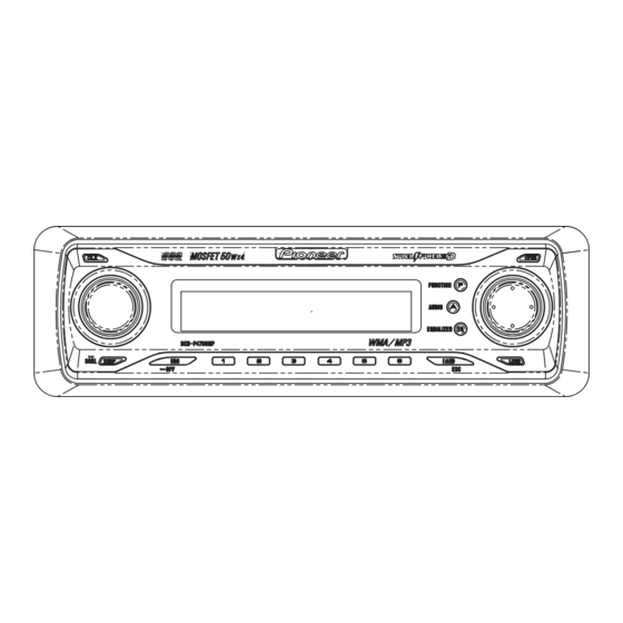
Page 10: Exterior
2.2 EXTERIOR DEH-P4750MP/XM/GS... - Page 11 (1) EXTERIOR SECTION PARTS LIST Mark No. Description Part No. Mark No. Description Part No. Button(OPEN) See Contrast table(2) Screw BMZ30P040FZK Screw BSZ26P060FTC Button(1-6) XAC7070 Screw BSZ30P060FTC XAC7071 Button(FUNCTION, AUDIO, EQ) Screw BSZ30P200FTC Spring XBH7001 Cable CDE7189 Cover XNS7087 XXA7310 Sub Button Assy(UP, DOWN, LEFT, RIGHT) Case CNB2793...
- Page 12 (2) CONTRAST TABLE DEH-P4750MP/XM/GS, DEH-P4790MP/XM/ID and DEH-P4770MP/XM/CS are constructed the same except for the following: Mark Description DEH-P4750MP/XM/GS DEH-P4790MP/XM/ID DEH-P4770MP/XM/CS Tuner Amp Unit CWM9777 CWM9777 CWM9895 Pin Jack(CN351) CKB1059 CKB1059 CKB1054 Holder CND1237 CND1237 CND1238 Detach Grille Assy CXC3891 CXC4374 CXC3893 LCD(LCD1) CAW1852...
- Page 13 DEH-P4750MP/XM/GS...
-
Page 14: Cd Mechanism Module
2.3 CD MECHANISM MODULE 1GEM1024 2GEM1045 3GEM1035 DEH-P4750MP/XM/GS... - Page 15 CD MECHANISM MODULE SECTION PARTS LIST Mark No. Description Part No. Mark No. Description Part No. Gear CNV8379 CD Core Unit(S10.1) CWX3096 Connector(CN101) CKS4182 Gear CNV8380 Connector(CN901) CKS4017 Gear CNV8381 Screw BMZ20P035FTC Gear CNV8382 Screw BSZ20P040FTC Gear CNV8383 Gear CNV8384 Screw(M2x4) CBA1362 Screw(M2x3)
-
Page 16: Block Diagram And Schematic Diagram
3. BLOCK DIAGRAM AND SCHEMATIC DIAGRAM 3.1 BLOCK DIAGRAM TUNER AMP UNIT 10 9 8 18 19 20 21 FM/AM TUNER UNIT IC 5 IC 3 EEPROM 3.3V 5.0V ANTENNA CN401 AM ANT FMRF IC 2 2.5V IC 1 FM ANT 3.3V IC 431 NJM4558MD... - Page 17 CN351 RESET R Lch REAR OUTPUT RST2 IC 651 Q352 BD4834G (DEH-P4770MP/XM/CS) F Lch FRONT OUTPUT Q351 TUNPDO TUNPDO SP601 TUNPDI TUNPDI TUNPCK TUNPCK VDD 5V REG Q901 TUNPCE1 TUNPCE2 Q902 SYSTEM CONTROLLER IC 601(1/2) PE5465A DALMON CN981 IC 431 BACKUP SENSE B.UP NJM4558MD...
-
Page 18: Overall Connection Diagram(Guide Page)
3.2 OVERALL CONNECTION DIAGRAM(GUIDE PAGE) Note: When ordering service parts, be sure to refer to " EXPLODED VIEWS AND PARTS LIST" or "ELECTRICAL PARTS LIST". Large size SCH diagram Guide page Detailed page CN901 FM(30%) : -31dB AM(30%) : -31dB IP-BUS : 2.2dB CD-DA, MP3 : 0.2dB mute... - Page 19 TUNER AMP UNIT FRONT R CH FRONT L CH REAR R CH REAR L CH > FM(30%) : -6.66dB AM(30%) : -6.66dB IP-BUS : 9.54dB CD-DA, MP3 : 9.54dB FM(30%) : -5.9dB AM(30%) : -5.9dB IP-BUS : 10.3dB CD-DA, MP3 : 10.3dB POWER AMP BEEP 600µH...
- Page 20 DEH-P4750MP/XM/GS...
- Page 21 DEH-P4750MP/XM/GS...
- Page 22 DEH-P4750MP/XM/GS...
- Page 23 DEH-P4750MP/XM/GS...
-
Page 24: Keyboard Unit
3.3 KEYBOARD UNIT LCD DRIVER/ KEY CONTROLLER DEH-P4750MP/XM/GS... - Page 25 KEYBOARD UNIT DISPLAY FUNCTION CLOCK LOUDNESS VOLUME : The power supply is shown with the marked box. DEH-P4750MP/XM/GS...
-
Page 26: Cd Mechanism Module(Guide Page)
3.4 CD MECHANISM MODULE(GUIDE PAGE) PICKUP UNIT(P10)(SERVICE) M1 CXC4440 SPINDLE MOTOR M2 CXB8933 LOADING /CARRIAGE CD DRIVER MOTOR DEH-P4750MP/XM/GS... - Page 27 SWITCHES: CD CORE UNIT(S10.1) S901:HOME SWITCH..ON-OFF S903:DSCSNS SWITCH..ON-OFF S904:12EJ SWITCH.....ON-OFF S905:8EJ SWITCH....ON-OFF The underlined indicates the switch position. SIGNAL LINE FOCUS SERVO LINE TRACKING SERVO LINE CARRIAGE SERVO LINE SPINDLE SERVO LINE CD CORE UNIT(S10.1) 3.3V REGULATOR SRAMLEVEL2 MICRO COMPUTER 3V REGULATOR CN721 SRAMLEVEL1...
- Page 28 DEH-P4750MP/XM/GS...
- Page 29 DEH-P4750MP/XM/GS...
- Page 30 DEH-P4750MP/XM/GS...
- Page 31 DEH-P4750MP/XM/GS...
- Page 32 - Waveforms Note : 1. The encircled numbers denote measuring points in the circuit diagram. 2. Reference voltage REFO1(1.65V) 1 DSCSNS 1 DSCSNS 1 DSCSNS 5V/div 500ms/div 5V/div 500ms/div 5V/div 500ms/div 2 8SNS 5 CLCONT 2 8SNS 5V/div 5V/div 5V/div 3 12SNS 4 LOEJ 3 12SNS...
- Page 33 0 FIN @ TE % RFAGC 500mV/div 200ms/div 500mV/div 2ms/div 1V/div 500µs/div # FE % RFAGC @ TE 500mV/div 500mV/div 500mV/div 9 TIN 500mV/div Focus Search waveform Track Open waveform 1 Track Jump waveform Ref.: Ref.: Ref.: REFO REFO REFO Mode: Mode: Mode:...
- Page 34 7 SIN % RFAGC 1V/div 500ms/div 1V/div 500µs/div 8 CIN 9 TIN 500mV/div 1V/div 9 TIN @ TE 500mV/div 1V/div 0 FIN 1V/div CD-ROM >> CD-DA mode change(Band key) Black dot(800µm) during play Ref.: Ref.: REFO REFO Mode: Mode: Normal Normal DEH-P4750MP/XM/GS...
- Page 35 DEH-P4750MP/XM/GS...
-
Page 36: Pcb Connection Diagram
4. PCB CONNECTION DIAGRAM 4.1 TUNER AMP UNIT NOTE FOR PCB DIAGRAMS TUNER AMP UNIT 1.The parts mounted on this PCB include all necessary parts for several destination. For further information for respective destinations, be sure to check with the schematic dia- CORD ASSY gram. - Page 37 SIDE A (DEH-P4770MP/XM/CS) FRONT REAR OUTPUT OUTPUT ORD ASSY ANTENNA CN1950 FRONT DEH-P4750MP/XM/GS...
- Page 38 TUNER AMP UNIT DEH-P4750MP/XM/GS...
- Page 39 SIDE B DEH-P4750MP/XM/GS...
-
Page 40: Keyboard Unit
4.2 KEYBOARD UNIT KEYBOARD UNIT SIDE A DEH-P4750MP/XM/GS... - Page 41 KEYBOARD UNIT SIDE B CN1951 DEH-P4750MP/XM/GS...
-
Page 42: Cd Core Unit(S10.1)
4.3 CD CORE UNIT(S10.1) CD CORE UNIT(S10.1) SIDE A LOADING /CARRIAGE MOTOR SPINDLE MOTOR CN721 HOME REFO1 DEH-P4750MP/XM/GS... - Page 43 CD CORE UNIT(S10.1) SIDE B 12EJ DSCSNS DEH-P4750MP/XM/GS...
-
Page 44: Panel Unit
4.4 PANEL UNIT SIDE B PANEL UNIT SIDE A PANEL UNIT CN831 EJECT DEH-P4750MP/XM/GS... -
Page 45: Electrical Parts List
5. ELECTRICAL PARTS LIST NOTE: Parts whose parts numbers are omitted are subject to being not supplied. • The part numbers shown below indicate chip components. • Chip Resistor RS1/_S___J,RS1/__S___J Chip Capacitor (except for CQS..) CKS.., CCS.., CSZS..The > mark found on some component parts indicatesthe importance of the safety factor of the part. •... - Page 46 Circuit Symbol and No. Part No. Circuit Symbol and No. Part No. R 301 (B,115,122) RS1/16S153J R 651 (A,57,68) RS1/16S183J R 302 (A,126,129) RS1/16S103J R 652 (A,56,70) RS1/16S102J R 303 (A,126,131) RS1/16S103J R 701 (A,58,41) RS1/16S221J R 304 (A,124,131) RS1/16S331J R 702 (A,58,31) RS1/16S221J...
- Page 47 Circuit Symbol and No. Part No. Circuit Symbol and No. Part No. C 205 (A,70,82) CEJQ2R2M50 C 751 (B,18,60) CKSRYB224K10 C 206 (A,70,88) CEJQ2R2M50 C 752 (B,12,50) CKSRYB102K50 C 207 (A,70,76) CEJQ2R2M50 C 753 (A,12,48) CEJQ101M16 C 208 (A,69,93) CEJQ2R2M50 C 761 (B,26,38) CKSRYB473K50...
- Page 48 Circuit Symbol and No. Part No. Circuit Symbol and No. Part No. Unit Name:Panel Unit S 10 (A,132,11) Switch CSG1173 S 11 (A,7,34) Switch CSG1173 S 12 (A,113,3) Switch CSG1174 MISCELLANEOUS S 13 (A,65,3) Switch CSG1174 D 1970 (A,26,5) LED CL220PGC S 14 (A,141,21) Switch...
- Page 49 Circuit Symbol and No. Part No. Circuit Symbol and No. Part No. R 307 (A,36,85) RS1/16SS183J C 217 (A,28,12) CKSSYB104K10 R 308 (A,32,83) RS1/16SS183J C 218 (A,25,7) CKSSYB473K10 R 309 (A,38,89) RS1/16SS183J R 310 (A,35,88) RS1/16SS183J C 219 (A,34,7) CKSSYB104K10 R 601 (B,43,59) RS1/16S101J...
-
Page 50: Adjustment
6. ADJUSTMENT 6.1 CD ADJUSTMENT 1) Cautions on adjustments 2) Test mode • In this product the single voltage (3.3V) is used for the This mode is used to adjust the CD mechanism module. regulator. The reference voltage is the REFO1 (1.65V) •... - Page 51 - Flow Chart [4]+[6]+Reset or [KEY] [4]+[6]+BU+ACC Contents Test Mode In Display [CD]or[SOURCE] Source On [BAND] RF AMP SPINDLE Power On Power On (T.Offset is not adjusted) Gain switching Speed switching (T.Offset is adjusted) [BAND] [→] [←] Tracking Servo Focus Close Focus Mode Automatic adjustment CRG+...
-
Page 52: Checking The Grating After Changing The Pickup Unit
6.2 CHECKING THE GRATING AFTER CHANGING THE PICKUP UNIT • Note : The grating angle of the PU unit cannot be adjusted after the PU unit is changed. The PU unit in the CD mechanism module is adjusted on the production line to match the CD mechanism module and is thus the best adjusted PU unit for the CD mechanism module. - Page 53 Ech → Xch 20mV/div, AC Grating waveform Fch → Ych 20mV/div, AC 0° 30° 45° 60° 75° 90° DEH-P4750MP/XM/GS...
-
Page 54: Error Mode
6.3 ERROR MODE - Error Messages Error is displayed with number for Error cause when CD is inoperative or stops with Error during operation. The purpose is to reduce nonsense calls from users as well as to assist all related analysis and repair for defects at service station. -
Page 55: System Microcomputer Test Program
6.4 SYSTEM MICROCOMPUTER TEST PROGRAM - PCL Output In the normal operation mode (with the detachable panel installed, the ACC switched ON, the standby mode cancelled), shift the TESTIN (Pin 5) terminal to H. The clock signal is output from the PCL terminal (Pin 62). The frequency of the clock signal is 786.432kHz that is one 16th of the fundamental frequency. -
Page 56: General Information
7. GENERAL INFORMATION 7.1 DIAGNOSIS 7.1.1 DISASSEMBLY Removing the Case (not shown) 1. Remove the Case. CD Mechanism Module Removing the CD Mechanism Module (Fig.1) Remove the four screws. Disconnect the connector and then remove the CD Mechanism Module. Removing the Grille Assy (Fig.1) Remove the two screws and then remove the Grille Assy. - Page 57 - How to hold the Mechanism Unit 1. Hold the top and bottom frame. 2. Do not squeeze top frame's front portion too tight, because it is fragile. Do not squeeze. - Removing the Upper and Lower Frames 1. With a disc clamped, remove the four springs (A), Upper Frame the two springs (B), the two springs (C), and the four screws.
- Page 58 - Removing the Pickup Unit 1. Apply shorting solder to the Pickup flexible cable. Disconnect the cable. 2. Set the mechanism to the clamp mode. 3. Remove the lead wires from the inner holder. 4. Remove the washer, styling holder, change arm, and pickup lock arm.
-
Page 59: Connector Function Description
7.1.2 CONNECTOR FUNCTION DESCRIPTION POWER SUPPLY, SPEAKER OUTPUT Pin No. Pin No. B.REM B.UP IP-BUS Pin No. Pin No. BUS L+ INPUT BUS+ ASENB BUS R+ INPUT BUS R- INPUT BUS L- INPUT BUS- DEH-P4750MP/XM/GS... -
Page 60: Parts
7.2 PARTS 7.2.1 IC - Pin Functions (PE5465A) Pin No. Pin Name Function and Operation swvdd Grille : Chip enable output Not used Test program mode input TESTIN Not used LCDPW Telephone mute input TELIN ejectin Eject sense input Flap illumination output FLPILM dalmon For consumption low-current output... - Page 61 Pin No. Pin Name Function and Operation Model select input MODELIN Flap close sense input CSENS Not used 78-81 A/D converter power supply terminal AVDD A/D converter reference voltage terminal AVREF AVSS IP-BUS : Data input IP-BUS : Data output Not used 88,89 dsens...
- Page 62 - Pin Functions(PD6340A) Pin No. Pin Name Function and Operation SEG4-0 LCD segment output COM3-0 LCD common output VLCD LCD drive power supply 11-14 KST3-0 Key strobe output 15,16 KDT0,1 Key data input (analogue input) Remote control reception input DPDT Display data input Not used KYDT...
- Page 63 - Pin Functions(UPD63763GJ) Pin No. Pin Name Function and Operation D.VDD Power supply for digital circuits D1.GND GND for 1.6V digital circuits reset Input of reset AB12-8 Address bus 12-8 from the microcomputer 9-16 AD7-0 Address/data bus 7-0 to the microcomputer Chip selection ASTB Address strobe...
- Page 64 Pin No. Pin Name Function and Operation D.VDD Power supply for digital circuits Output of focus drive PWM + Output of focus drive PWM - Output of tracking drive PWM + Output of tracking drive PWM - Output of thread drive PWM + Output of thread drive PWM - Output of spindle drive PWM + Output of spindle drive PWM -...
- Page 65 - Pin Functions(PE5454A) Pin No. Pin Name Format Function and Operation AVREF A power supply Positive power supply(5V) AVSS A power supply GND RFOK Output of state of RFOK Not used EVDD E power supply Positive power supply 6, 7 Not used IC/FLMD0 IC : VSS direct connection/FLMOD0 : Pull-down...
- Page 66 Pin No. Pin Name Format Function and Operation xread CD LSI read control signal output XASTB CD LSI address strobe output BVSS B power supply GND BVDD B power supply Positive power supply 71-83 AD0-12 Address/data Bus 0-12 84-86 Not used FMODE For flash rewriting Connected to VSS via the resistor FLRQ...
- Page 67 - FM/AM Tuner Unit 10 9 8 18 19 20 21 IC 5 IC 3 EEPROM 3.3V 5.0V AM ANT FMRF IC 2 2.5V IC 1 FM ANT 3.3V FMRF MIXER, IF AMP DET, FM MPX RF adj ANT adj CF52 CF51 IC 4...
-
Page 68: Display
7.2.2 DISPLAY - LCD(CAW1852)(DEH-P4750MP/XM/GS, DEH-P4790MP/XM/ID) - LCD(CAW1851)(DEH-P4770MP/XM/CS) DEH-P4750MP/XM/GS... -
Page 69: Operational Flow Chart
7.3 OPERATIONAL FLOW CHART Power ON VDD=5V Pin 19, 41 bsens Pin 93 bsens=L asens Pin 92 asens=L dsens Pin 90 dsens=L ASENSBO←H Pin 71 CSENS < < - CSENS 2V, 3V CSENS Pin 77 Last source returns. 2V < CSENS < 3V CD loading functions are available. -
Page 70: Cleaning
7.4 CLEANING Before shipping out the product, be sure to clean the following portions by using the prescribed cleaning tools: Portions to be cleaned Cleaning tools CD pickup lenses Cleaning liquid : GEM1004 Cleaning paper : GED-008 DEH-P4750MP/XM/GS... -
Page 71: Operations
8. OPERATIONS DEH-P4750MP/XM/GS... - Page 72 DEH-P4750MP/XM/GS...
- Page 73 DEH-P4750MP/XM/GS...
- Page 74 DEH-P4750MP/XM/GS...
- Page 75 DEH-P4750MP/XM/GS...
- Page 76 DEH-P4750MP/XM/GS...
- Page 77 DEH-P4750MP/XM/GS...
- Page 78 Fixing the front panel If you do not operate the removing and attaching the front panel function, use the supplied fixing screws and holders to fix the front panel to this unit. 1. Attach the holders to both sides of the front panel. Holder CXX1644 Holder...
- Page 79 - Connection Diagram(DEH-P4750MP/XM/GS, DEH-P4790MP/XM/ID) DEH-P4750MP/XM/GS...
- Page 80 - Connection Diagram(DEH-P4770MP/XM/CS) DEH-P4750MP/XM/GS...
- Page 81 DEH-P4750MP/XM/GS...
- Page 82 - Jigs List Name Jig No. Remarks Test Disc TCD-782 Checking the grating L.P.F. Checking the grating g (Two pieces) DEH-P4750MP/XM/GS...
Need help?
Do you have a question about the DEH-P5780MP and is the answer not in the manual?
Questions and answers