Table of Contents
Advertisement
Quick Links
Advertisement
Table of Contents

Subscribe to Our Youtube Channel
Related Manuals for Sylvania LC320SS8


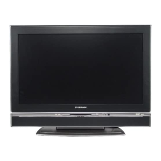
Summary of Contents for Sylvania LC320SS8
- Page 1 SERVICE MANUAL 32″ COLOR LCD TELEVISION LC320SS8...
-
Page 2: Table Of Contents
IMPORTANT SAFETY NOTICE Proper service and repair is important to the safe, reliable operation of all Funai Equipment. The service procedures recommended by Funai and described in this service manual are effective methods of performing service operations. Some of these service special tools should be used when and as recommended. -
Page 3: Specifications
SPECIFICATIONS < TUNER / NTSC > ANT. Input ---------------------- 75 ohm Unbal., F type Description Condition Unit Nominal Limit 1. AFT Pull In Range ±2.3 ±2.1 TV.ch.4 dBµ 2. Syncronizing Sens. CA.ch.31 dBµ CA.ch.87 dBµ < TUNER / ATSC > Description Condition Unit... - Page 4 < AUDIO > All items are measured across 8 Ω load at speaker output terminal with L.P.F. / Video1 Input. Description Condition Unit Nominal Limit 1. Audio Output Power 10% THD: Lch/Rch 10.0/10.0 9.0/9.0 2. Audio Distortion 500mW: Lch/Rch 0.5/0.5 2.0/2.0 -6dB: Lch 100 to 11 k...
-
Page 5: Important Safety Precautions
IMPORTANT SAFETY PRECAUTIONS Prior to shipment from the factory, our products are strictly inspected for recognized product safety and electrical codes of the countries in which they are to be sold. However, in order to maintain such compliance, it is equally important to implement the following precautions when a set is being serviced. - Page 6 3. Design Alteration Warning - Do not alter or add 7. Product Safety Notice - Some electrical and to the mechanical or electrical design of this TV mechanical parts have special safety-related receiver. Design alterations and additions, characteristics which are often not evident from including, but not limited to circuit modifications visual inspection, nor can the protection they give and the addition of items such as auxiliary audio...
- Page 7 Precautions during Servicing A. Parts identified by the # symbol are critical for safety. Replace only with part number specified. B. In addition to safety, other parts and assemblies are specified for conformance with regulations applying to spurious radiation. These must also be replaced only with specified replacements.
- Page 8 Safety Check after Servicing Examine the area surrounding the repaired location for damage or deterioration. Observe that screws, parts and wires have been returned to original positions. Afterwards, perform the following tests and confirm the specified values in order to verify compliance with safety standards. 1.
-
Page 9: Standard Notes For Servicing
STANDARD NOTES FOR SERVICING Circuit Board Indications How to Remove / Install Flat Pack-IC 1. The output pin of the 3 pin Regulator ICs is 1. Removal indicated as shown. With Hot-Air Flat Pack-IC Desoldering Machine: Top View Bottom View 1. - Page 10 3. The flat pack-IC on the CBA is affixed with glue, so With Soldering Iron: be careful not to break or damage the foil of each 1. Using desoldering braid, remove the solder from pin or the solder lands under the IC when all pins of the flat pack-IC.
- Page 11 2. Installation With Iron Wire: 1. Using desoldering braid, remove the solder from 1. Using desoldering braid, remove the solder from all pins of the flat pack-IC. When you use solder the foil of each pin of the flat pack-IC on the CBA flux which is applied to all pins of the flat pack-IC, so you can install a replacement flat pack-IC more you can remove it easily.
- Page 12 Instructions for Handling Semi- conductors Electrostatic breakdown of the semi-conductors may occur due to a potential difference caused by electrostatic charge during unpacking or repair work. 1. Ground for Human Body Be sure to wear a grounding band (1 MΩ) that is properly grounded to remove any static electricity that may be charged on the body.
-
Page 13: Cabinet Disassembly Instructions
CABINET DISASSEMBLY INSTRUCTIONS 1. Disassembly Flowchart Removal Step/ Remove/*Unhook/ This flowchart indicates the disassembly steps for the Loc. Part Fig. Unlock/Release/ cabinet parts, and the CBA in order to gain access to Note Unplug/Unclamp/ item(s) to be serviced. When reassembling, follow the Desolder steps in reverse order. - Page 14 [4] Rear Cabinet (S-4) (S-5) (S-4) (S-4) (S-1) (S-4) (S-5) (S-1) (S-1) [3] Stand Cover (S-1) (S-4) [2] Stand Hinge [1] Stand Base Plate (S-3) (S-2) (S-2) (S-3) Fig. D1 A71F0DC...
- Page 15 [9] Digital Main CBA Unit [7] Jack Holder(D) Earth Plate (S-10) (S-9) (S-8) [8] Shield Box Shield Plate (N-1) (S-6) (S-11) (S-6) (S-7) [6] Power Supply CBA (S-6) (S-7) (S-6) [5] Chassis Bracket Fig. D2 A71F0DC...
- Page 16 [14] Panel Holder (S-15) (S-16) (S-15) [10] Jack Holder (A) [11] Jack CBA (S-12) (S-15) (S-13) Desolder (S-16) [13] Junction CBA (S-15) (S-14) [12] Inverter CBA (S-14) Fig. D3 A71F0DC...
- Page 17 [20] Front Cabinet [16] LCD Module Assembly [19] Speaker (S-21) [18] IR Sensor (S-18) (S-20) Shield Plate (S-17) [19] Speaker (S-17) (S-17) [15] T-CON CBA (S-21) (S-19) (S-18) [17] Function CBA Fig. D4 A71F0DC...
- Page 18 TV Cable Wiring Diagram Jack CBA CN7501 To LCD Module Assembly Function CBA CN9002 CN9001 CN102 CN9005 CN9003 To LCD T-CON CBA Module Assembly Digital Main Junction Inverter CBA CBA Unit CN552 CN3018 CN3023 CN3002 CN1050 CN3001 CL552B CN1100 CN1150 CL552A CN1200 CN3010 CN3014...
-
Page 19: Electrical Adjustment Instructions
ELECTRICAL ADJUSTMENT INSTRUCTIONS General Note: “CBA” is abbreviation for How to set up the service mode: “Circuit Board Assembly.” Service mode: Note: Electrical adjustments are required after 1. Use the service remote control unit. replacing circuit components and certain mechanical parts. It is important to perform 2. - Page 20 1. Purity Check Mode 2. VCOM Adjustment This mode cycles through full-screen displays of red, *This adjustment is required when reparing T-CON green, blue, and white to check for non-active pixels. CBA. 1. Enter the Service mode. Test Point Adj. Point 2.
- Page 21 The following adjustment normally are not attempted in 5. [CUTOFF] the field. Only when replacing the LCD Panel then adjust Press [3] button to select “COB” for Blue Cutoff as a preparation. adjustment. Press [1] button to select “COR” for Red Cutoff adjustment.
-
Page 22: How To Initialize The Lcd Television
HOW TO INITIALIZE THE LCD TELEVISION How to initialize the LCD television: 1. Turn the power on. 2. To enter the service mode, press the service button on the service remote control unit. (Refer to page 5-1.) - To cancel the service mode, press [POWER] button on the remote control unit. -
Page 23: Block Diagrams
BLOCK DIAGRAMS System Control Block Diagram A71F0BLS... - Page 24 Video Block Diagram A71F0BLV...
- Page 25 Audio-1 Block Diagram A71F0BLA1...
- Page 26 Audio-2 Block Diagram A71F0BLA2...
- Page 27 Digital Signal Process Block Diagram A71F0BLD...
- Page 28 Inverter Block Diagram A71F0BLINV...
- Page 29 Power Supply Block Diagram A71F0BLP...
-
Page 30: Schematic Diagrams / Cba's And Test Points
SCHEMATIC DIAGRAMS / CBA’S AND TEST POINTS Standard Notes WARNING Many electrical and mechanical parts in this chassis have special characteristics. These characteristics often pass unnoticed and the protection afforded by them cannot necessarily be obtained by using replacement components rated for higher voltage, wattage, etc. - Page 31 LIST OF CAUTION, NOTES, AND SYMBOLS USED IN THE SCHEMATIC DIAGRAMS ON THE FOLLOWING PAGES: 1. CAUTION: CAUTION: FOR CONTINUED PROTECTION AGAINST RISK OF FIRE, REPLACE ONLY WITH SAME TYPE_A,_V FUSE. ATTENTION: UTILISER UN FUSIBLE DE RECHANGE DE MÊME TYPE DE_A,_V. 2.
- Page 32 Power Supply 1/2 Schematic Diagram NOTE: The voltage for parts in hot circuit is measured using hot GND as a common terminal. VOLTAGE CHART CN301 Pin No. Voltage 12.2 12.2 15.6 34.6 A71F0SCP1...
- Page 33 Power Supply 2/2 Schematic Diagram NOTE: The voltage for parts in hot circuit is measured using hot GND as a common terminal. VOLTAGE CHART CN302 Pin No. Voltage A71F0SCP2...
- Page 34 Inverter & Junction Schematic Diagram VOLTAGE CHART CAUTION ! CN552 Fixed voltage (or Auto voltage selectable) power supply circuit is used in this unit. NOTE: Pin No. Voltage CAUTION ! : For continued protection against risk of fire, If Main Fuse (F501) is blown , check to see that all components in the power supply The voltage for parts in hot circuit is measured using replace only with same type 4 A, 125V fuse.
- Page 35 Jack Schematic Diagram VOLTAGE CHART CN7501 Pin No. Voltage A71F0SCJ...
- Page 36 Function Schematic Diagram VOLTAGE CHART CN102 Pin No. Voltage A71F0SCF...
- Page 37 IR Sensor Schematic Diagram A71F0SCIR...
- Page 38 Digital Main 1/9 Schematic Diagram A71F0SCD1...
- Page 39 Digital Main 2/9 Schematic Diagram 1 NOTE: The order of pins shown in this diagram is different from that of actual IC3015. IC3015 is divided into four and shown as IC3015 (1/4) ~ IC3015 (4/4) in this Digital Main Schematic Diagram Section. 8-10 A71F0SCD2...
- Page 40 Digital Main 3/9 Schematic Diagram 1 NOTE: The order of pins shown in this diagram is different from that of actual IC3015. IC3015 is divided into four and shown as IC3015 (1/4) ~ IC3015 (4/4) in this Digital Main Schematic Diagram Section. 8-11 A71F0SCD3...
- Page 41 Digital Main 4/9 Schematic Diagram 1 NOTE: The order of pins shown in this diagram is different from that of actual IC3015. IC3015 is divided into four and shown as IC3015 (1/4) ~ IC3015 (4/4) in this Digital Main Schematic Diagram Section. A71F0SCD4 8-12...
- Page 42 Digital Main 5/9 Schematic Diagram 1 NOTE: The order of pins shown in this diagram is different from that of actual IC3015. IC3015 is divided into four and shown as IC3015 (1/4) ~ IC3015 (4/4) in this Digital Main Schematic Diagram Section. A71F0SCD5 8-13...
- Page 43 Digital Main 6/9 Schematic Diagram A71F0SCD6 8-14...
- Page 44 Digital Main 7/9 Schematic Diagram A71F0SCD7 8-15...
- Page 45 Digital Main 8/9 Schematic Diagram 8-16 A71F0SCD8...
- Page 46 Digital Main 9/9 Schematic Diagram A71F0SCD9 8-17...
- Page 47 Power Supply CBA Top View Because a hot chassis ground is present in the power NOTE: supply circuit, an isolation transformer must be used. The voltage for parts in hot circuit is measured using Also, in order to have the ability to increase the input hot GND as a common terminal.
- Page 48 Power Supply CBA Bottom View Because a hot chassis ground is present in the power NOTE: supply circuit, an isolation transformer must be used. The voltage for parts in hot circuit is measured using Also, in order to have the ability to increase the input hot GND as a common terminal.
- Page 49 Inverter CBA Top View NOTE: The voltage for parts in hot circuit is measured using hot GND as a common terminal. CAUTION ! Fixed voltage (or Auto voltage selectable) power supply circuit is used in this unit. Because a hot chassis ground is present in the power CAUTION ! : For continued protection against risk of fire, If Main Fuse (F501) is blown , check to see that all components in the power supply...
- Page 50 Inverter CBA Bottom View NOTE: The voltage for parts in hot circuit is measured using hot GND as a common terminal. CAUTION ! Fixed voltage (or Auto voltage selectable) power supply circuit is used in this unit. Because a hot chassis ground is present in the power CAUTION ! : For continued protection against risk of fire, If Main Fuse (F501) is blown , check to see that all components in the power supply...
- Page 51 Jack CBA Top View BA71F0F01021-4 8-22...
- Page 52 Jack CBA Bottom View PIN 6 OF PIN 8 OF PIN 9 OF PIN 14 OF CN7501 CN7501 CN7501 CN7501 PIN 5 OF PIN 3 OF PIN1 OF CN7501 CN7501 CN7501 8-23 BA71F0F01021-4...
- Page 53 Function CBA Top View Function CBA Bottom View BA71F0F01021-2 8-24...
- Page 54 IR Sensor CBA Top View Junction CBA Top & Bottom View BA71F0F01041 IR Sensor CBA Bottom View BA71F0F01021-3 8-25...
-
Page 55: Waveforms
WAVEFORMS WF1 ~ WF7 = Waveforms to be observed at Waveform check points. (Shown in Schematic Diagram.) Input: NTSC Color Bar Signal (with 1kHz Audio Signal) Pin 1 of CN7501 Pin 5 of CN7501 CVBS 0.2V 20µs VIDEO-Pb 0.2V 20µs Pin 9 of CN7501 Pin 6 of CN7501 20µs... -
Page 56: Wiring Diagram
WIRING DIAGRAM 10-1 A71F0WI... -
Page 57: Exploded Views
EXPLODED VIEWS Cabinet Jack CBA LCD Module Assembly CL7501 SP802 T-CON CBA CL3023 CLN802 CLN101 B28 B6 IR Sensor CBA Function CBA SP801 CLN801 CLN102 Digital Main CBA Unit Junction Power Supply CBA Inverter CBA See Electrical Parts List AC501 for parts with this mark. - Page 58 Packing Packing Tape Some Ref. Numbers are not in sequence. Packing Tape Packing Tape Tape Packing Tape Packing Tape Packing Tape 11-2 A71F0PEX...
-
Page 59: Mechanical Parts List
MECHANICAL PARTS LIST PRODUCT SAFETY NOTE: Products marked with a Ref. No. Description Part No. # have special characteristics important to safety. ASSEMBLED SCREW ( D9 M3X6 ) A71F0UH 1EM424392 Before replacing any of these components, read SCREW S-TIGHT M3X8 BIND HEAD+ GBHS3080 carefully the product safety notice in this service HEX SCREW #4-40 7MM... -
Page 60: Electrical Parts List
ELECTRICAL PARTS LIST PRODUCT SAFETY NOTE: Products marked with a Ref. No. Description Part No. # have special characteristics important to safety. C639 ELECTROLYTIC CAP . 1000µF/50V M CE1JMZPDL102 Before replacing any of these components, read C640 ELECTROLYTIC CAP . 22µF/16V M CE1CMASDL220 carefully the product safety notice in this service C642... - Page 61 Ref. No. Description Part No. Ref. No. Description Part No. C864 CHIP CERAMIC CAP .(1608) B K 0.1µF/50V CHD1JK30B104 D663 SWITCHING DIODE 1SS133(T-77) QDTZ001SS133 C865 CHIP CERAMIC CAP .(1608) B K 0.1µF/50V CHD1JK30B104 D664 SWITCHING DIODE 1SS133(T-77) QDTZ001SS133 C866 CHIP CERAMIC CAP .(1608) B K 0.1µF/50V CHD1JK30B104 D665 SWITCHING DIODE 1SS133(T-77)
- Page 62 Ref. No. Description Part No. Ref. No. Description Part No. CARBON RES. 1/4W J 390k Ω CARBON RES. 1/4W J 100k Ω R607 RCX4JATZ0394 R688 RCX4JATZ0104 CARBON RES. 1/4W J 150 Ω CARBON RES. 1/4W J 10k Ω R608 RCX4JATZ0151 R689 RCX4JATZ0103 CARBON RES.
- Page 63 Ref. No. Description Part No. Ref. No. Description Part No. CAPACITORS CAPACITORS C108 CHIP CERAMIC CAP .(1608) F Z 0.1µF/50V CHD1JZ30F104 C7001 ELECTROLYTIC CAP . 47µF/16V M H7 CE1CMAVSL470 C109 CHIP CERAMIC CAP .(1608) F Z 0.1µF/50V CHD1JZ30F104 C7002 CHIP CERAMIC CAP .(2125) F Z 10µF/10V CHE1AZ30F106 C110 CHIP CERAMIC CAP .(1608) F Z 0.1µF/50V...
- Page 64 Ref. No. Description Part No. Ref. No. Description Part No. RESISTORS JK7705 JACK SW DIN PCB L DIN-435C JYEL040YUQ02 CHIP RES. 1/10W J 10k Ω JK7706 JACK SW RCA PCB L 05 RCA-340NI-01 JYRL030YUQ14 R7001 RRXAJR5Z0103 CHIP RES. 1/10W J 10k Ω JK7711 JACK RCA PCB S 03 RCA-347HT-03 JXRJ030YUQ01...
- Page 65 Ref. No. Description Part No. Ref. No. Description Part No. C1046 CHIP CERAMIC CAP .(1608) B K 1µF/25V CHD1EK30B105 CONNECTORS C1061 CAP CERAMIC HV 15pF/3.15KV/SL/J CCD3FJASL150 CN501 CONNECTOR B2P3-VH(LF)(SN) J3VH020JG001 C1062 CHIP CERAMIC CAP . B K 1500pF/50V CHD1JK30B152 CN1050 CONNECTOR/JACK 1747386-1 JB17J02AP002 C1063...
- Page 66 Ref. No. Description Part No. Ref. No. Description Part No. D1163 SWITCHING DIODE 1SS133(T-77) QDTZ001SS133 Q1100 FET POWER MOS SMD NP22N055SLE-E1-AZ QF2ZNP22N055 D1164 SWITCHING DIODE 1SS133(T-77) QDTZ001SS133 Q1101 FET POWER MOS SMD NP22N055SLE-E1-AZ QF2ZNP22N055 D1165 SWITCHING DIODE 1SS133(T-77) QDTZ001SS133 Q1102 FET POWER MOS SMD NP22N055SLE-E1-AZ QF2ZNP22N055 D1166 SWITCHING DIODE 1SS133(T-77)
- Page 67 Ref. No. Description Part No. Ref. No. Description Part No. CARBON RES. 1/4W J 51k Ω CHIP RES. 1/10W F 750 Ω R1014 RCX4JATZ0513 R1216 RRXAFR5H7500 CHIP RES.(1608) 1/10W F 5.1k Ω CHIP RES. 1/10W J 5.1k Ω R1015 RRXAFR5H0512 R1217 RRXAJR5Z0512 CHIP RES.
- Page 68 Ref. No. Description Part No. BC501 BEADS INDUCTOR FBR07HA121SB-00 LLBF00STU030 BC502 BEADS INDUCTOR FBR07HA121SB-00 LLBF00STU030 BC552 BEADS INDUCTOR FBR07HA121SB-00 LLBF00STU030 BC553 BEADS INDUCTOR FBR07HA121SB-00 LLBF00STU030 BC1000 PCB JUMPER D0.6-P5.0 JW5.0T BC1001 BEADS INDUCTOR FBR07HA121SB-00 LLBF00STU030 BC1050 PCB JUMPER D0.6-P12.5 JW12.5T BC1051 PCB JUMPER D0.6-P12.5 JW12.5T...
- Page 69 Misuse of any trademarks or any other content in this manual is strictly prohibited. Funai shall aggressively enforce its intellectual property rights to the fullest extent of the law. LC320SS8 A71F0UH 2007-04-19...
Need help?
Do you have a question about the LC320SS8 and is the answer not in the manual?
Questions and answers