Advertisement
Quick Links
Full Color LED Controller Driver with PWM Control
GENERAL DESCRIPTION
The NJU6062 is a full color LED controller driver. It can
control and drive a 3 in 1 packaged (Red, Green and
Blue) LED.
The NJU6062 contains PWM luminance (Pulse Width
Modulation) control circuit , LED driving circuit, MPU
interface.
The PWM signal control the duty cycle of each RGB
LED delicately, therefore can recognize a lot of colors.
Enable terminal (ON/OFF) is possible to synchronize
with a sound source..
It requires only four external components such as three
resistors for LED current adjustment, which enables the
NJU6062 to save PCB space.
Multi Device control is enabled and it is possible to
control the multiple NJU6062 by a I
The NJU6062 is suitable for cellular phone, car audio
and so on.
FEATURES
Controlling a 3-in-1 packaged RGB LED
4-channel output
Built-in PWM luminance control
2
Built-in I
C interface circuit
Multi Device control
Built-in CR oscillation circuit
Operating voltage
Package
CMOS Technology
2
C address.
I
=30mA x 4
LED
(256steps x 4)
1.8V to 5.5V
FFP12(2.0*2.0*0.85mm), SSOP14
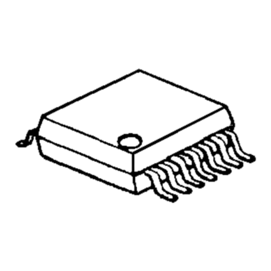
PACKAGE OUTLINE
NJU6062PB1
(FFP12)
NJU6062
NJU6062V
(SSOP14)
- 1 -
Advertisement

Related Manuals for JRC NJU6062

Summary of Contents for JRC NJU6062
- Page 1 Full Color LED Controller Driver with PWM Control GENERAL DESCRIPTION PACKAGE OUTLINE The NJU6062 is a full color LED controller driver. It can control and drive a 3 in 1 packaged (Red, Green and Blue) LED. The NJU6062 contains PWM luminance (Pulse Width Modulation) control circuit , LED driving circuit, MPU interface.
-
Page 2: Pin Descriptions
Output Reset terminal - Active “L”. Input "L" status: Reset state RSTb "H" status: Operating state Multi Device control terminal (connect RSTb of next NJU6062 for Output DATAOUT Multi Device use.) External clock input terminal Input It is used by external clock. -
Page 3: Block Diagram
(1) Description for Each Blocks (1-1) PWM Luminance Control The NJU6062 incorporates four 256 steps PWM Luminance Control circuits. At the user’s option, PWM data can be set. PWM data set by selecting start point(S) and end point(E) of each terminal. - Page 4 NJU6062 (1-2) Oscillator The oscillation circuit with the internal register and capacitor generates the clock signal for PWM. The oscillation circuit can be turned on/off by the instruction to minimize the current consumption. The oscillation frequency (fosc) can be selected in 16 conditions by the instruction.
- Page 5 NJU6062 Instructions The data transfer between CPU and the NJU6062 is via a I C interface. Table.1 shows the instruction codes of the NJU6062. Table 1. Instruction Code * : Don’t Care Code Lower Instruction Description address AL : Address increment...
- Page 6 NJU6062 (2-1) Explanation of Instruction Code Lower address: 00h ~ 09h. It is incremented within the loop 05h ~ 09h. Therefore, until the stop condition is reached, it is possible to write instructions that from the LED1 endpoint to the...
- Page 7 NJU6062 (2-2) Instruction Code (a) Function Set This instruction set the Address increment, Oscillation set PWM output select Function. Lower address Lower address increment set Set the increment of the address of the write data. It is possible to write the PWM data without address setting.
- Page 8 NJU6062 External clock input mode set The NJU6062 can be operated with external clock input without using internal oscillation circuit. In the case of using external clock, set D =”H”, and enter it from the OSC terminal. 0 : Internal Oscillator use(Default)
- Page 9 NJU6062 Update / Static on This instruction is active PWM data to LED terminal output / LED terminal is made "H" regardless of PWM data. Lower address ~ UD : Update Set the update of PWM data of each LED terminal.
- Page 10 SDA terminal. 3. R/W condition NJU6062 is only for slave LSI, and the data D0 in the first byte(at eighth bit timing) should be ”0”. 4. Upper address Second bite defines the Upper address, it outputs the acknowledge just after the ninth bit timing through the SDA terminal.
- Page 11 10, I C interface reset (3) Multi Device control It is possible to control multiple NJU6062 by a I C address. Connect the DATAOUT and RSTb terminal, and Multi Device control is enabled by assigning a unique address to each device in default configuration.
- Page 12 NJU6062 (5-1) Multi Device control Initialization frow (Multi Device address set) Ex.)NJU6062 x 3 devices REGISTER REGISTER SLAVE ADDRESS UPPER LOWER INPUT DATA +R/W ADDRESS ADDRESS Set the upper address of device1 to 01h. RSTb=”L” Therefore, device2 and 3 are not responding.
- Page 13 NJU6062 After reset upper address Initial value : 00h • Device 1 Device 2 Device 3 DATAOUT DATAOUT DATAOUT RSTb SCL SDA RSTb SCL SDA RSTb SCL SDA “L” “H” “L” “L” RSTb After address set Initialization • Device 1...
- Page 14 NJU6062 ABSOLUTE MAXIMUMN RATINGS Ta=25°C PARAMETERS SYMBOL CONDITIONS RATINGS UNIT VDD Power Supply VDD terminal -0.3 to +7.0 Driver Off Break Down Voltage LED1, LED2, LED3,LED4 terminals offmax Driver On Break Down Voltage LED1, LED2, LED3,LED4 terminals onmax RSTb, SCL, SDA, OSC, Input Voltage -0.3 to V...
- Page 15 NJU6062 DC ELECTRICAL CHARACTERISTICS(V =1.8V / 3.0V / 5.5V, Ta= 25˚C) PARAMETERS SYMBOL CONDITIONS Unit Input Input”H”Level SCL, SDA1 0.7V Voltage1 Input”H”Level RSTb, EN 0.8V Voltage2 Input”L”Level SCL, SDA 0.3V Voltage1 Input”L”Level RSTb, EN 0.2V Voltage2 Input”H”Level RSTb, SCL V µA...
- Page 16 NJU6062 AC ELECTRICAL CHARACTERISTICS(V =1.8V / 3.0V / 5.5V, Ta= 25˚C) PARAMETERS SYMBOL CONDITIONS Unit C Bus Timing (V =3.0V / 5.5V) SCL Clock Frequency Hold Time(Repeat) SCL, SDA HD;STA “START”Condition SCL clock ”L”Pulse width SCL clock ”H”Pulse width HIGH Repeat ”START”...
- Page 17 NJU6062 LED Terminal Enable timing =1.8V LED1~4, LED Terminal Enable Time =3.0V =5.5V CL=10pF, =1.8V RL=1KΩ LED Terminal Disable Time =3.0V =5.5V =1.8V DATAOUT, Output Delay Time CL=10pF =3.0V =5.5V Reset Timing Reset ”L” Pulse width RSTb Reset Time RSTb Multi Device access timing =1.8V...
- Page 18 NJU6062 (1) I C Bus timing SU;DAT HD;STA SU;SAT SU;STO HD;STA HD;DAT HIGH S : Start condition Sr : Repeat Start condition P : Stop condition (2) LED terminal enable timing LED1 to 4 (3) Reset timing RSTb (4) Multi Device access timing Set to Upper address •...
- Page 19 NJU6062 (5) External clock Note) All timing V voltage level. - 19 -...
-
Page 20: Application Circuit
NJU6062 APPLICATION CIRCUIT Example 1 LED4 LED3 LED2 LED1 NJU6062 RSTb Resistor Selection LED Current Control Resistor LED Voltage LED Forward Voltage (@I Output “L” Level Voltage (@I LED Forward Current Example) I = 30mA, V = 5.0V, V = 2.0V(@I = 30mA), V =0.5V... - Page 21 NJU6062 Example 2 (Cascade connect) LED4 LED3 NJU6062 LED2 RSTb LED1 DATAOUT LED4 LED3 NJU6062 LED2 RSTb LED1 DATAOUT LED4 LED3 NJU6062 LED2 RSTb LED1 DATAOUT [Note] For use in the Multi Device control connection, use the same power supply for V...
- Page 22 NJU6062 Example 3 (PWM output select ) LED4 LED3 LED2 LED1 NJU6062 RSTb DATAOUT (LED input Dr.) PWN input SHDNb [CAUTION] The specifications on this databook are only given for information , without any guarantee as regards either mistakes or omissions. The...
Need help?
Do you have a question about the NJU6062 and is the answer not in the manual?
Questions and answers