Panasonic SB-WA340 Service Manual
Active subwoofer system
Hide thumbs
Also See for SB-WA340:
- Operating instructions manual (48 pages) ,
- Operating instructions manual (44 pages) ,
- Operating instructions manual (44 pages)

Related Manuals for Panasonic SB-WA340


Summary of Contents for Panasonic SB-WA340
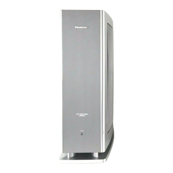
- Page 1 ORDER NO. MD0310441C2 Active Subwoofer System SB-WA340EBS1 Colour (S1)...Silver Type...
-
Page 2: Specifications
SPECIFICATIONS Specification Active subwoofer Type 1 way, 1 speaker system, bass- ref. Woofer 17 cm cone type Impedance Output sound pressure level 80 dB/W (1.0 m) Frequency range 40 Hz-220 Hz (-16 dB) 45 Hz-180 Hz (-10 dB) Dimensions (W x H x D) 160 x 450 x 424 mm Mass Approx. -
Page 3: Leakage Current Cold Check
1. When servicing, observe the original lead dress. If a short circuit is found, replace all parts which have been overheated or damaged by the short circuit. 2. After servicing, see to it that all the protective devices such as insulation barriers, insulation papers shields are properly installed. -
Page 4: Handling The Lead-Free Solder
each point. 5. Reverse the AC plug in the AC outlet and repeat each of the above measurements. 6. The potential at any point should not exceed 0.75 volts RMS. A leakage current tester (Simpson Model 229 or equivalent) may be used to make the hot checks, leakage current must not exceed 1/2 milliamp. -
Page 5: Connection Of The Speaker Cables
the amplifier are used. If this occurs, follow the procedure outlines below: 1. Turn off the power. 2. Determine the cause of the problem and correct it. 3. Turn on the power once again after one minute. Note : When the protection circuitry functions, the unit will not operate unless the power is first turned off and then on again. - Page 6 Some chassis components may have sharp edges. Be careful when disassembling and servicing. 1. This section describes procedures for checking the operation of the major printed circuit boards and replacing the main components. 2. For reassembly after operation checks or replacement, reverse the respective procedures.
- Page 7 Step 2: Remove all screws. Step 3: Remove the Stand Base. Step 4: Remove all screws from the speaker bottom. Step 5: Pull the Power/Amp Unit as shown.
- Page 8 Step 6: Release the connector CN506 and pull out the Power/Amp Unit. Step 7: Push the Net Frame from two holes inside the unit. Step 8: Remove the Net Frame. Step 9: Remove all the screws.
- Page 9 Step 10: Remove the Speaker. Step 11 & 12: Remove all the screws. Step 13: Release the connector CN507. Step 14: Remove the 2 screws.
- Page 10 Step 15 & 16: Remove all the screws. Step 17: Place the Power PCB as shown for checking. Checking for AC Inlet PCB. 6.2. Main Component Replacement Procedures...
-
Page 11: Connection Of The Speaker Wiring
6.2.1. Replacement of the Power IC Step 1 & 2: Remove all the screws. Step 3: Desolder the Power IC terminal and replace the component. 7. Connection of the Speaker Wiring 8. Block Diagram... -
Page 12: Schematic Diagram
9. Schematic Diagram (All schematic diagrams may be modified at any time with the development of the new technology) Note: - The voltage value and waveforms are the reference voltage of this unit measured by DC electronic voltmeter (high impedance) and oscilloscope on the basis of chassis. - Page 13 When replacing any of these components, be sure to use only manufacturer’s specified parts shown in the parts list. - The parenthesized indications in the Remarks columns specify the areas or colour. (Refer to the cover page for area or colour) Parts without these indications can be used for all areas.
- Page 14 13.1.2. Cabinet Parts List...
- Page 15 Ref. No. Part No. Part Name & Description Remarks CABINET AND CHASSIS RFKHBWA302-S SPK CABINET ASS’Y RMG0520-KJ CATCH SRTF4B10F SCREW RGK1601-S STAND ORNAMENT RMQ0705 EVA PACKING RKA0147-K FOOT RYB0298A NET FRAME ASS’Y XTB4+12AFZ SCREW (WOOFER) RGNX0175M-S SPEC LABEL REM0072-3 RGR0332A-KA REAR PANEL RHD30092 SCREW (MAIN PCB)
-
Page 16: Line Filter
Ref. No. Part No. Part Name & Description Remarks Q516 KRC102MTA TRANSISTOR Q517 KTC2026 TRANSISTOR Q519 KTC3199GRTA TRANSISTOR Q520 KRA102MTA TRANSISTOR DIODES D500 B0AACK000004 DIODE D501 B0JAPG000019 DIODE D502 B0JAPG000019 DIODE D503 MA2C700A0F DIODE D504 B0AACK000004 DIODE D505 B0AACK000004 DIODE D506 B0AACK000004 DIODE... - Page 18 Ref. No. Part No. Part Name & Description Remarks T501 G4C7AGG00001 POWER TRANSFORMER T502 G4C2AAJ00005 BACK-UP TRANSFORMER COMPONENT COMBINATION Z501 ERZV10V511CS ZENER SPEAKER EAST17PL21B6 SPEAKER RELAY RLY501 RSY0040M-0 PRIMARY RELAY FUSES K5D202BK0005 250V 2A FUSE FUSE HOLDERS FC501 EYF52BC FUSE HOLDER FC502 EYF52BC FUSE HOLDER...
- Page 20 Ref. No. Part No. Part Name & Description Remarks RESISTORS R401 ERDS2TJ224T 220K 1/4W R402 ERDS2TJ102T 1K 1/4W R403 ERDS2TJ104T 100K 1/4W R501 ERDS2TJ472T 4.7K 1/4W R502 ERDS2TJ472T 4.7K 1/4W R503 ERDS2TJ153T 15K 1/4W R504 ERDS2TJ153T 15K 1/4W R505 ERDS2TJ153T 15K 1/4W R506 ERDS2TJ153T...
- Page 21 Ref. No. Part No. Part Name & Description Remarks R550 ERDS2TJ103T 10K 1/4W R551 ERDS2TJ472T 4.7K 1/4W R552 ERDS2TJ562T 5.6K 1/4W R553 ERDS2TJ563T 56K 1/4W R554 ERDS2TJ824T 820K 1/4W R555 ERDS2TJ104T 100K 1/4W R556 ERDS2TJ103T 10K 1/4W R557 ERDS2TJ563T 56K 1/4W R558 ERDS1FVJ180T 18 1/2W...
- Page 22 Ref. No. Part No. Part Name & Description Remarks C507 ECBT1H180JC5 18P 50V C508 ECBT1H180JC5 18P 50V C509 ECBT1H220JC5 22P 50V C510 ECBT1H220JC5 22P 50V C511 ECBT1H220JC5 22P 50V C512 ECBT1H220JC5 22P 50V C513 F1D1H473A012 0.047 50V C514 ECA0JM101B 100 6.3V C515 ECKR2H103ZF5 0.01 500V...
-
Page 23: Packing Materials
Ref. No. Part No. Part Name & Description Remarks C563 ECQV1H823JL3 0.082 50V C564 ECBT1C122KR5 1200P 16V C565 F1D1H1040002 0.1 50V C566 F1D1H1040002 0.1 50V C567 ECA1HM100B 10 50V C568 ECBT1C103NS5 0.01 16V C569 F1D1H473A012 0.047 50V 13.3. Packing Materials & Accessories Parts List Ref. - Page 24 FLE0310/D/A/S/E/N...
- Page 25 CN501 7..1 CP502 JK502 LED P.C.B. CN507 SPEAKER JK501 WOOFER H505A/W505 SOLDER SIDE SOLDER SIDE POWER P.C.B. SOLDER SIDE T501(POWER TRANSFORMER) TRANSFORMER P.C.B. T502(POWER TRANSFORMER) AC INLET AC IN JK500 P.C.B. 230~240V 50HZ CN502 SOLDER SIDE 7.
- Page 26 IC501 RSN311W64B-P POWER HIC POWER CONTROL CIRCUIT POWER CONTROL/PROTECTION CIRCUIT 12(11) (25) (19) D501 D502 Q506 INTERFACE SWITCH TO MAIN BLOCK Q505 (JK700) OF SA-HT1000EB/EG-S SWITCHING SL(R)/SURRL(R) FILTER FILTER JK501(JK502) SURROUND SPEAKER CCH/CENTRE FILTER FILTER JK502 CENTRE SPEAKER FILTER SUBWOOFER FL(R)/FRONTL(R) FILTER FILTER...
- Page 27 C0AABB000055 KRA102MTA RSN311W64B-P KTA12710YTA KTC3199GRTA KRC102MTA B0AACK000004 KTC2026 MA2C700A0F B0HARM000017 B0BA9R600002 Cathode Cathode Anode Anode B0EAKM000085 B0BA6R600008 SLI325URCT31 B0JAPG000019 B0BA5R100013 Cathode Anode Cathode Cathode Anode Anode...
- Page 28 POWER P.C.B. (REPX0375C) CAUTION RISK OF ELECTRIC SHOCK AC VOLTAGE LINE. PLEASE DO NOT TOUCH THIS P.C.B J570 CN501 J581 J528 R543 CP502 R544 7 6 5 4 3 2 1 R540 Q513 R539 Q507 C537 R542 J504 R572 R554 R541 J533 Q506...
- Page 29 Q507 C537 R554 J505 C541 J513 Q508 Q510 Q501 J544 Q520 R570 J402 D518 J403 J567 J586 J568 J404 J587 J569 J405 J588 J560 J406 J417 R527 J584 R502 R517 R504 Q503 R508 R598 C511 R507 R503 R528 R567 D533 R568 C517 C543...
- Page 30 AC INLET P.C.B. (REPX0375C) CAUTION RISK OF ELECTRIC SHOCK AC VOLTAGE LINE. PLEASE DO NOT TOUCH THIS P.C.B FC502 FC501 F1 250V T2AL T502 (POWER TRANSFORMER) L500 JK500 Q516 AC IN J500 RLY501 C555 J501 230V-240V R589 50HZ C557 R578 C558 J502 J503...
- Page 31 SCHEMATIC DIAGRAM-1 : MAIN SIGNAL LINE : -B SIGNAL LINE POWER CIRCUIT : +B SIGNAL LINE IC501 C551 IC501 0.01 RSN311W64B-P POWER HIC E501 K4CZ01000027 R501 R513 4.7K R502 C507 18P 4.7K R514 C508 18P R524 120K R506 D501-D502 B0JAPG000019 R516 R526 R505...
- Page 32 SCHEMATIC DIAGRAM-2 : MAIN SIGNAL LINE : -B SIGNAL LINE POWER CIRCUIT : +B SIGNAL LINE R597 R594 C564 1200P Q514 R592 R403 R599 Q513 100K C565 R593 R571 C568 R591 R572 3.3K 0.01 6.8K 470K C562 IC502 5600P C0AABB000055 C524 C525 DUAL LOW-NOISE OP AMP...
-
Page 33: Transformer Circuit
SCHEMATIC DIAGRAM-3 : -B SIGNAL LINE : +B SIGNAL LINE C555 R589 35V4.7 Q516 R578 KRC102MTA SYNC SWITCH CN502 R580 PCONT Q517 POWER CIRCUIT KTC2026 (CP502) ON SYNC R587 VOLTAGE REGULATOR D530 D528 SCHEMATIC 2.7K SYS6V DIAGRAM-2 C559 HELP 0.01 C556 R588 0.01...
Need help?
Do you have a question about the SB-WA340 and is the answer not in the manual?
Questions and answers