Advertisement
B5B-7248-00
RA044<Rev.001>
9 S ERVICE MANUAL
2016
COPYRIGHT © 2016 JVC KENWOOD Corporation
1
PRECAUTION. . . . . . . . . . . . . . . . . . . . . . . . . . . . . . . . . . . . . . . . . . . . . . . . . . . . . . . . . . . . . . . . . . . . . . . . . 1-5
2
SPECIFIC SERVICE INSTRUCTIONS . . . . . . . . . . . . . . . . . . . . . . . . . . . . . . . . . . . . . . . . . . . . . . . . . . . . . . 1-5
3
DISASSEMBLY . . . . . . . . . . . . . . . . . . . . . . . . . . . . . . . . . . . . . . . . . . . . . . . . . . . . . . . . . . . . . . . . . . . . . . 1-24
4
ADJUSTMENT . . . . . . . . . . . . . . . . . . . . . . . . . . . . . . . . . . . . . . . . . . . . . . . . . . . . . . . . . . . . . . . . . . . . . . . 1-28
5
TROUBLESHOOTING . . . . . . . . . . . . . . . . . . . . . . . . . . . . . . . . . . . . . . . . . . . . . . . . . . . . . . . . . . . . . . . . . 1-44
This product complies with the RoHS directive for the European market.
B5B-7248-00
SERVICE MANUAL
144/430MHz DUAL BANDER
COPYRIGHT © 2016 JVC KENWOOD Corporation
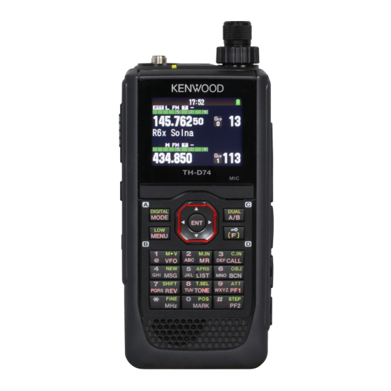
TH-D74E
TABLE OF CONTENTS
This product uses Lead Free solder.
No.RA044<Rev.001>
2016/9
Advertisement

Related Manuals for Kenwood TH-D74E


Summary of Contents for Kenwood TH-D74E
-
Page 1: Table Of Contents
B5B-7248-00 TH-D74E COPYRIGHT © 2016 JVC KENWOOD Corporation TABLE OF CONTENTS PRECAUTION............... . . 1-5 SPECIFIC SERVICE INSTRUCTIONS . - Page 2 Neither is any liability assumed for damages resulting from the use of the information contained herein. JVC KENWOOD Corporation reserves the right to make changes to any products herein at any time for improvement purposes. Bluetooth Copyrights The Bluetooth word mark and logos are registered trademarks owned by Bluetooth SIG, Inc.
- Page 3 RECEIVER Band A Band B Circuitry F3E, F2D, F1D, F7W Double Super Heterodyne A1A, A3E, J3E Triple Super Heterodyne IF Frequency 1st IF 57.15 MHz 58.05 MHz 2nd IF 450 kHz 450 kHz 3rd IF (A1A, A3E, J3E) 10.8 kHz Sensitivity (TYP.) Amateur Band 12dB SINAD,...
- Page 4 TRANSMITTER RF Power Output EXT.PS 13.8 V / Battery:7.4 V 0.5 W 0.05 W Modulation Reactance Modulation GMSK Reactance Modulation Modulation Deviation ±5.0 kHz ±2.5 kHz Spurious Emissions HI / MID -60 dBc or less -50 dBc or less -40 dBc or less Microphone Impedance 2 k ohm TTFF (Cold start)
-
Page 5: Precaution
Circuit Description 2.1.1 Outline The TH-D74E is an FM dual-band transceiver designed for amateur radio applications in the 144/430 MHz bands. 2.1.2 Frequency Configuration This transceiver has two discrete VCO/PLL and IF circuit configurations for the A-band and B-band to achieve simultaneous dual-band signal reception and full-duplex operation. - Page 6 2.1.3 Receiver System 2.1.3.1 VHF receiver circuit A band VHF receiver circuit The reception signal from the antenna passes through the filter circuit and enters the RF amplifier (Q179). The signal amplified by the RF amplifier (Q179) enters the distribution circuit for signal distribution with the B-band. The distributed signal is amplified by the second RF amplifier (Q178), passes through the band-pass filter, and enters the mixer (Q281).
- Page 7 B band UHF receiver circuit The reception signal from the antenna passes through the filter circuit and enters the RF amplifier (Q172). The signal amplified by the RF amplifier (Q172) enters the distribution circuit for signal distribution with the A-band. The distributed signal is amplified by the second RF amplifier (Q192), passes through the band-pass filter, and enters the mixer (IC283).
- Page 8 BAR Antenna circuit The bar antenna can be selected for HF reception. The reception signal from the bar antenna passes through the tuning circuit and enters the RF amplifier (Q190). Then the signal is received on the same path in the HF receiving circuit. BAND B 3 IF 10.8k BAR ANT...
- Page 9 2.1.4.3 Thermal protection circuit The sub MPU (IC661) monitors the detected voltage (FTH) of the thermistor (TH1) arranged for the prevention of the thermal breakdown of the final amplifier (Q2) in use. An APC voltage (OAGCA/APC) change will occur when the temperature exceeds the preset temperature, at which time the TX power will be controlled to prevent excessive heat generation.
- Page 10 2.1.5.4 Unlock detection circuit The LD pins (pin 39 of the IC284 and pin 7 of the IC364) of the PLL ICs will output L-level signals when the PLLs are unlocked. The main MPU (IC702) is in control of the switching timing of transmission and reception by monitoring the output. CONT PCB CODEC IC IC707...
- Page 11 2.1.6.2 Lithium-ion Battery charging control circuit The IC585 will charge the lithium battery by receiving the charge control instruction from the main MPU. The IC585 will detect the battery voltage and the battery charging current, and operate as shown below. If the battery voltage is less than 6.0 V, the IC585 and Q580 will supply a constant voltage of 6.0 V to the +B power supply, and control the gate voltage of the Q581 and perform pre-charging at a charging current of 128 mA.
- Page 12 IC882 6.8V_AVR (From TXRX PCB) AFBS IC731 6.8V_AVR 6.8V (From TXRX PCB) For LEDs LAMPS 31BU 3.1V_AVR IC717 IC723 1.2V_AVR (From TXRX PCB) 3.3V_AVR 12BU IC714 33AD CN703 BUTTON BATT 1.8V_AVR IC708 /33ADS 3.3V_AVR IC712 Q704 MODAMP MODBS 1.8V_DCDC IC718 Q884 MICB IC724...
- Page 13 FM tuner circuit The FM broadcasting band (76MHz~108MHz) signal can be received using an SMA antenna. The reception signal passes through the band-pass filter and enters the RF amplifier (Q675) for the amplification of the signal, and the signal is applied to the FM tuner IC (IC674). The signal is demodulated in the FM tuner IC to generate an audio signal and de-emphasized.
- Page 14 2.1.8.2 Memory Circuit The memory circuit consists of the main processor (IC702), mobile DDR (IC701), and flash memory (IC705). The flash memory has a capacity of 256 Mbits, including a transceiver control program and recording data for the MPU. The mobile DDR is has a capacity of 512 Mbits.
- Page 15 MAIN MPU GPS / BT IC IC702 IC935 FL932 BT ANT (METAL LINE) /BT_SHUTDOWN /GPS_SHUTDOWN LEVEL CONVERTER IC937 33BT 18BT BT_AUD_DO 18BT_AUD_IN BT_AUD_DI 18BT_AUD_OUT AUDIO BCLK 18BT_AUD_CLK WCLK 18BT_AUD_FSYNC LEVEL CONVERTER IC936 33BT 18BT TXD2 18BT_HCI_RX RXD2 18BT_HCI_TX HCI I/F RTS2 18BT_HCI_CTS CTS2...
- Page 16 COMPONENTS DESCRIPTION Ref. No. Use / Function Operation/Condition/Compatibility 2.2.1 TX-RX UNIT (XC1-138E-01) IC701 LPDDR Program for operation Ref. No. Use / Function Operation/Condition/Compatibility IC702 Main MPU CPU with DSP RF AMP TX AMP IC703 Reset 3.5V detect IC704 /BINT 5.0V detect IC281 IF(A-band) A-band...
- Page 17 Ref. No. Use / Function Operation/Condition/Compatibility Ref. No. Use / Function Operation/Condition/Compatibility Q383 RF AMP Buffer DC SW VHF TX Q384 RF AMP Fin A-band DC SW Q385 RIPPLE FILTER VCO A-band Q171 RF AMP UHF RX A-band Q386 Oscillator VCO A-band Q172 RF AMP...
- Page 18 Ref. No. Use / Function Operation/Condition/Compatibility Ref. No. Use / Function Operation/Condition/Compatibility D29,30 TX AMP on/off D379 Speed up Ripple filter RF SW UHF TX D380 Modulator A-band VCO Shift D32,35 RF SW VHF TX D381 Modulator A-band VCO D33,36 RF SW UHF TX D382...
- Page 19 Pin No. Name Function Pin No. Name Function BD11 I/O LCD driver bus data output BPFA O Band A BPF adjustment signal BD10 I/O LCD driver bus data output I 47C power supply BD09 I/O LCD driver bus data output I Band A audio signal BD08 I/O LCD driver bus data output...
- Page 20 Pin No. Name Function Pin No. Name Function ENC2 I Encoder data 2 CN501(to VCO A) - GND VCO_A I Band A VCO signal ENC1 I Encoder data 1 Fin_A O Band A PLL RF input signal - GND 2.3.2 TX-RX UNIT (XC1-138)(2/7) TX-RX - GND Pin No.
- Page 21 2.3.4 TX-RX UNIT (XC1-138)(4/7) VCO-B Pin No. Name Function Pin No. Name Function I2CCKR O I2C CLK signal for radio IC CN400(to TX-RX) - GND VCO2 I Band B switch signal for I2CDTR I/O I2C DATA signal for radio IC power supply(VCO2) - GND CV_B...
- Page 22 Pin No. Name Function CN183(to BARANT) I SW signal - GND I MW signal 2.3.6 TX-RX UNIT (XC1-138)(6/7) BARANT Pin No. Name Function CN184(to MW/SW) O MW signal - GND O SW signal 2.3.7 TX-RX UNIT (XC1-138)(7/7) KEY Pin No. Name Function CN1(to CONTROL)
- Page 23 2.3.8 Micro USB Socket J700 Pin No. Pin Name Function Rating and Condition V BUS V BUS sense input Input voltage 4.4-5.25V I/O USB D- Full-Speed(12Mbps) VIH>2.0V,VIL<0.8V Included Pull up resistors I/O USB D+ Full-Speed(12Mbps) VIH>2.0V,VIL<0.8V 2.3.9 micro SD Slot J701 Pin No.
-
Page 24: Disassembly
SECTION 3 DISASSEMBLY How to Remove the Case Assembly (1) Remove the SP/MIC cap <1>. <2> (2) Pull out the two knobs <2>. <2> (3) Remove the two screws <3> on the front case. (4) Remove the nut <4> of the antenna receptacle. (5) Remove the nut <5>... - Page 25 Precautions for Disassembly 3.3.3 Remove the top cover from the shield cover (1) Use tweezers to slightly lift the edge of the top cover. <1> 3.3.1 How to Remove Key Tops (2) As you do step 2 above, vary the position you hold the top (1) The key tops are pasted to the surface of the front case cover as you lift it, and remove the top cover <2>.
- Page 26 Precautions for Reassembly 3.4.3 Mounting of Top Panel Nuts and Front Case Screws (1) Assemble the front case into the chassis and attach the two 3.4.1 Mounting of Bluetooth Antenna (BAR SPRING) nuts to the top panel. (1) Mount the Bluetooth antenna onto the front-side groove of (2) Attach the two screws to the front case.
- Page 27 3.4.5 Assembly Information (Sheet/Cushion) When “Main Parts” is changed (ordered), “Assembled Sheet / Cushion” should also be changed (ordered) together. The Sticker and Sheet etc are non-reusable parts. It requires the new one to get the radio’s performance after repairs. For example, when “Mounting bracket (J2B-0201-00)”...
-
Page 28: Adjustment
Battery Jig (W3F-0208-00) (s). Update the firmware according to the procedure displayed in updating program. Download the latest updating program from the following URL: http://www.kenwood.com/i/products/info/amateur/ software_download.html * The URL may change without notice. Required Test Equipment + Terminal(Red) + Terminal(Red) - Page 29 Connection cable Adjustment Mode Connection cable consists of 2 pieces of flat cable assembly Outline (X42-3510-10), to extend its cable length double for connection (1) Set the transceiver to adjustment mode and change each between two PCBs. setting data item. For repair and adjustment, use this connection cable to connect (2) This mode is used when the PCBs are replaced at a a Control PCB and a TX-RX PCB by inserting the connection...
- Page 30 LCD display in the adjustment mode Major items and service setup Minor items (">" will appear when selected) Adjustment frequency Value stored in the transceiver Present value RSSI value (displayed only during BPF adjustment) * "TX Current" will appear during transmission power adjustment.
- Page 31 Adjustment items and Display Adjustment items Display Adjustment Major item Minor item Frequency adjustment 6th line displayed item number A. Power supply voltage (7.4 V) 0 COMMON Battery 439.900 MHz B. Transmission frequency Frequency B/S Off 439.900 MHz Frequency B/S On- 439.900 MHz C.
- Page 32 Adjustment items Display Adjustment Major item Minor item Frequency adjustment 6th line displayed item number F. MAX Deviation MAX Deviation VHF Frequency Center 145.100 MHz Frequency Low 144.100 MHz Frequency High 145.900 MHz MAX Deviation UHF Frequency Center 435.100 MHz Frequency Low 430.100 MHz Frequency High...
- Page 33 Adjustment Points TX-RX UNIT (2/7) Component side CV_B CV_A CV_A: VCO lock voltage (A-band) CV_B: VCO lock voltage (B-band) * Check the VCO lock voltage with the VCO shield case attached. Common Section Item Condition Measurement Adjustment Specifications /Remarks Test- Unit Terminal Unit Parts Method...
- Page 34 Item Condition Measurement Adjustment Specifications /Remarks Test- Unit Terminal Unit Parts Method equipment 2.Battery Voltage Goes to adjustment mode. Battery terminal [] or Note: The correct Adjust See "4.4 Adjustment Mode". [Write] transmission power 1) Battery terminal: 7.4V will not be output from the transceiver in user mode unless the battery voltage is...
- Page 35 Item Condition Measurement Adjustment Specifications /Remarks Test- Unit Terminal Unit Parts Method equipment 2. Power 13) Power:HI Power meter Encoder [] or 4.8W ±0.1W Frequency:435.100MHz Ammeter []/[] [Write] 2.18A or less Transmission 14) Power:HI Power meter Encoder [] or 4.8W ±0.1W Frequency:430.100MHz Ammeter []/[]...
- Page 36 Item Condition Measurement Adjustment Specifications /Remarks Test- Unit Terminal Unit Parts Method equipment 3. Balance TCXO 3)Frequency:145.900MHz Linear detector Encoder [] or 2.4kHz ±50Hz Linear detector Power meter []/[] [Write] (FM±) Oscilloscope LPF : 3kHz HPF : OFF Transmission 4)Frequency:435.100MHz Linear detector Encoder [] or...
- Page 37 Item Condition Measurement Adjustment Specifications /Remarks Test- Unit Terminal Unit Parts Method equipment 4. Balance VCO 6)Frequency:439.900MHz Linear detector Encoder [] or 2.4kHz ±50Hz Linear detector Power meter []/[] [Write] (FM±) Oscilloscope LPF : 15kHz HPF : OFF Transmission 5. MAX Deviation Battery terminal:7.4V/3.0A Linear detector Encoder...
- Page 38 Item Condition Measurement Adjustment Specifications /Remarks Test- Unit Terminal Unit Parts Method equipment 2.Power 2) Power: Hi Power meter Check 4.8W ±0.3W Frequency: 145.900MHz Ammeter 2.2A or less Transmission 3)Power: Mid Power meter Check 2.0W ±0.4W Frequency: 144.100MHz Ammeter 1.6A or less Transmission 4)Power: Mid Power meter...
- Page 39 Receiver Section: Adjustment Mode Setting Items Item Condition Measurement Adjustment Specifications /Remarks Test- Unit Terminal Unit Parts Method equipment 1.RX BPF 1)Frequency: 136.05MHz [Auto] Automatic Max RSSI value A-Band SSG: -110dBm(0.707μV) Oscilloscope adjustment Mode:FM(3kHz) Audio analyzer AF VR:0.63V/8 ohm 2)Frequency: 145.95MHz [Auto] Automatic Max RSSI value...
- Page 40 Item Condition Measurement Adjustment Specifications /Remarks Test- Unit Terminal Unit Parts Method equipment B-Band 17)Frequency: 469.95MHz [Auto] Automatic Max RSSI value SSG:-110dBm(0.707μV) Oscilloscope adjustment Mode:FM(3kHz) Audio analyzer AF VR:0.63V/8 ohm 2.IF Filter 1)Frequency: 145.953MHz [Auto] Automatic Calibration SSG:-53dBm(501μV) adjustment Mode:FM OFF 1)Frequency: 145.947MHz [Auto] Automatic...
- Page 41 Item Condition Measurement Adjustment Specifications /Remarks Test- Unit Terminal Unit Parts Method equipment HF-Band 6)Frequency: 51.100MHz [] or Write SQL Level1 [Write] SSG:-121dBm(0.2μV) SSG:-116dBm(0.35μV) S-FULL SSG: -101dBm(2μV) Mode: FM(3kHz) 4.10 Receiver Section: User Mode Confirmation Items Item Condition Measurement Adjustment Specifications /Remarks Test-...
- Page 42 Item Condition Measurement Adjustment Specifications /Remarks Test- Unit Terminal Unit Parts Method equipment B-Band 9) Frequency: 430.050MHz Check 12dB SINAD or more Mode: FM(3kHz) Audio analyzer SSG: -121dBm(0.19μV) Oscilloscope AF output: 0.63V/8 ohm ATT:OFF 10) Frequency: 430.050MHz Check 12dB SINAD or less Mode: FM(3kHz) Audio analyzer SSG: -115.5dBm (0.375μV)
- Page 43 Item Condition Measurement Adjustment Specifications /Remarks Test- Unit Terminal Unit Parts Method equipment 4.S-meter 1)Frequency: 145.950MHz Check One segment in A-Band Mode:FM(3kHz) S-meter lights. SSG: -120dBm(0.22μV)±5dB 2)SSG: -105dBm(1.26μV)±5dB Check All segments in S-meter light. 3)Frequency: 439.950MHz Check One segment in Mode:FM(3kHz) S-meter lights.
-
Page 44: Troubleshooting
SECTION 5 TROUBLESHOOTING Fault Diagnosis of the BGA (Ball Grid Array) IC Overview A flowchart for determining whether or not the transceiver can be powered on (the LCD does not function even if the power switch is turned on) due to broken BGA parts. BGA parts MAIN MPU(IC702), mobile DDR(IC701), Flash Memory(IC705) Checking Battery voltage... - Page 45 When a normal value is confirmed. If the /FRST is always 0V, the MAIN MPU is Checking the control signal output from the MAIN When an abnormal broken. Points to be checked value is confirmed. Normal voltage Remove D700 to check the voltage of Flash /FRST Memory side R762.
- Page 46 Failure diagnosis of the Bluetooth section Overview: When the Bluetooth function does not operate, use this flowchart to determine the problem. Major parts for a Bluetooth circuit • Bluetooth antenna • TCXO 19.2MHz (X930) • LC filter (FL932) • 32.768kHz clock (X931) •...
- Page 47 When a normal condition is confirmed. Replace defective parts of the reference generation When an abnormal When an abnormal Check reference CLK: X930 of the BT/GPS. circuit of BT/GPS as necessary. condition is confirmed. condition is confirmed. The BT/GPS (IC935) is defective. (Check with the BT turned ON).
- Page 48 Failure diagnosis of the GPS section Overview: When the GPS function does not operate, use this flowchart to determine the problem. Major parts for a GPS circuit • GPS Connector(CN931) • 33BT Regulator (IC932) • SAW Filter(FL931) • 18BT Regulator (IC931) •...
- Page 49 When a normal condition is confirmed. When an abnormal Check that the control signal Replace the RA937. The MPU/DSP (IC702) is condition is confirmed. (/GPS_SHUTDOWN) of the defective if the condition does not return to normal. GPS is at 1.8 V. (Check with the GPS Replace the control.
- Page 50 MEMO...
- Page 51 SCHEMATIC DIAGRAM TX-RX UNIT (XC1-138E-01) 1/7: CONTROL ENC Vol KEY(XC1-138 7/7) MONI POWER Micro 3.9V TL700 S722 S723 S721 S70-0514-05 S70-0514-05 S70-0514-05 * R155 TL701 Q712 E-01 VBUS TL702 3.3V TL722 E700 J700 F10-3236-05 EMD12 TH700 NCP18WB473J0S BUSY ON AIR SHIELD CASE TL721 GND2...
- Page 52 TX-RX UNIT (XC1-138E-01) 2/7: TX-RX R152 E-01 100k F577 L581 Q580 FZA10BQ-3R15 8.3V 8.4V L580 TL601 2.2u HS8K1 L579 Q579 LR79Z0HQ2R2M 3.15A L584 DC_IN 1 J576 L583 L582 R615 4.7u 0.01 2.2u DC IN C628 0.1u UT6K3 L588 40C DCDC D587 SURGE OR CIRCUIT...
- Page 53 BLOCK DIAGRAM Q886 EM6M2 GPS MODULE DACS CN706 CN661 E40-6421-15 E40-6422-15 MODAMP Q704 EM6M2 Bluetooth 2400-2483.5MHz 1575.42MHz MODS OMAP MICB VDCIN Q884 EM6M2 DDR_A[0]~DDR_A[13] IC702 MICBS 1.6A DDR_BA[0],DDR_BA[1] 512Mbit F579 J 5 7 6 DDR_CAS,DDR_CKE,DDR_CLKN E 0 3 - 0 1 7 0 - 0 5 FZA10AC-1R6 3.15A mDDR...
- Page 54 INTERCONNECTION DIAGRAM ENC Vol R3K-0001 2pin Cable XC1-138 7/7 E3D-0013 Speaker T07-0266 VCO-A VCO-B 16pin FFC 6pin FPC XC1-138 3/7 XC1-138 4/7 E3F-0139 J82-0114 50pin FPC X42-351 CN706 CN661 E40-6422-15 E40-6421-15 DET1 2 2 DET1 J700 E58-0566-05 16pin DET2 4 16pin 4 DET2 BtoB Connector...
- Page 55 TX-RX UNIT (XC1-138E-01) 3/7: VCO-A 3.2V RIPPLE Q385 FILTER DSC9A01/T/ SPEED UP R471 L407 OSCILLATOR FREQUENCY CONTROL Q386 C509 L413 D381 C542 MCH3914-H/8/ CV_A C520 C517 4.7u 1SV325FT Q381 C543 C527 R467 L411 2SC4726(P,Q) 270n Q383 0.01u 0.5p Q387 2SC4726(P,Q) RF AMP SSM3K15AMFV RF AMP...
- Page 56 TX-RX UNIT (XC1-138E-01) 4/7: VCO-B R424 VCO2 3.6V Q371 RE1C001ZP 33BF R425 VCO1 Q372 RE1C001ZP D366 MODULATOR R415 C448 0.5p OSCILLATOR RF AMP D369,D372 Q368 FREQUENCY MCH3914-H/8/ CONTROL C437 C423 L387 D369 C451 L378 C429 R503 220n Q389 1SV325FT 0.5p 470p RF SW 2SC5108FT/Y/...
- Page 57 TX-RX UNIT (XC1-138E-01) 5/7: MW/SW TX-RX(XC1-138 2/7) CN182 L216 470n 4.6V B-BAND 76-108MHz C155 C254 R166 RF SW 0.1u C139 L221 C280 D201 Q195 2SC5661/P/ 0.1u 0.1u 1SS390 RF AMP R145 Q197 D204 LTC043ZEBFS8 1SS390 R235 R238 C269 C267 4.7k 4.7k Q186,189 D197...
- Page 58 TX-RX UNIT (XC1-138E-01) 6/7: BARANT TX-RX UNIT (XC1-138E-01) 7/7: KEY CN184 S700 S70-0519-05 TL191 MW/SW(XC1-138 5/7) 21 Keys BARANT CN183 TL193 6.8V KEY Back Light KEY_O4 TL192 S701 S705 S709 S713 S717 S70-0519-05 S70-0519-05 S70-0519-05 S70-0519-05 S70-0519-05 KEY_O3 S702 S706 S710 S714 S718...
- Page 59 PRINTED CIRCUIT BOARD TX-RX UNIT (XC1-138E-01) 1/7: CONTROL --- Component side view (J7C-0229-00) --- R755 IC705 CN702 C792 IC721 C839 C834 C841 C840 IC930 R848 R930 C735 C738 C732 IC725 IC705 IC930 D675 RA671 C930 R782 C931 RA712 RA711 IC671 L710 C676 RA937...
- Page 60 TX-RX UNIT (XC1-138E-01) 1/7: CONTROL --- Foil side view (J7C-0229-00) --- RTCK S723 IC726 TL733 TL740 D720 C821 R860 R851 R815 R852 RA704 RA710 RA718 R737 R850 RA705 R814 RA715 IC672 C846 TL734 IC732 C869 C698 IC724 IC728 IC935 Q711 C838 IC673 R918...
- Page 61 TX-RX UNIT (XC1-138E-01) 2/7: TX-RX --- Component side view (J7C-0229-00) --- R150 C469 J-00 C584 R630 C471 C621 C622 IC578 C466 D578 R151 K-01 Q375 R250 C609 C338 IC284 R152 R627 R640 E-01 C190 C334 C330 C203 C339 IC583 D588 C329 L202 R592...
- Page 62 TX-RX UNIT (XC1-138E-01) 2/7: TX-RX --- Foil side view (J7C-0229-00) --- C160 C130 C125 C129 C135 C118 C154 C159 C399 C123 C122 C117 C136 Q362 C148 C153 R381 R382 C152 C102 L368 C150 C467 Q364 C481 C407 D362 C624 R426 R388 L366 C128...
- Page 63 A-1C ADDRESS TABLE OF BOARD PARTS Side Y axis Each address may have an address error by one X axis interval. REF.NO. LOCATION REF.NO. LOCATION REF.NO. LOCATION REF.NO. LOCATION REF.NO. LOCATION REF.NO. LOCATION REF.NO. LOCATION REF.NO. LOCATION REF.NO. LOCATION REF.NO. LOCATION REF.NO. LOCATION REF.NO. LOCATION REF.NO. LOCATION REF.NO. LOCATION REF.NO. LOCATION REF.NO. LOCATION REF.NO. LOCATION REF.NO. LOCATION Q363 B- 2B D177...
- Page 64 TX-RX UNIT (XC1-138E-01) 3/7: VCO-A --- Component side view (J7C-0229-00) --- --- Foil side view (J7C-0229-00) --- C530 R466 R468 L404 XC1-138 R453 C534 R463 R456 J7C-0229 C519 L401 Q381 C539 R462 C524 C516 ADDRESS TABLE OF BOARD PARTS R452 Each address may have an address error by one interval.
- Page 65 TX-RX UNIT (XC1-138E-01) 4/7: VCO-B --- Component side view (J7C-0229-00) --- --- Foil side view (J7C-0229-00) --- C462 R424 C456 R419 D372 D373 CN400 R420 L390 XC1-138 C451 C452 C445 C446 R415 R416 J7C-0229 D366 D367 C448 C449 R502 C440 C441 C442 C443...
- Page 66 TX-RX UNIT (XC1-138E-01) 5/7: MW/SW --- Component side view (J7C-0229-00) --- --- Foil side view (J7C-0229-00) --- CN183 D196 D200 C259 Q196 D202 R145 R144 R231 C155 D194 J7C-0229-00 R170 Q197 L221 C139 R234 C261 D195 R158 L198 XC1-138 R239 Q195 D201 C267...
- Page 67 TX-RX UNIT (XC1-138E-01) 6/7: BARANT --- Component side view (J7C-0229-00) --- --- Foil side view (J7C-0229-00) --- CN184 TL192 TL193 TL191 TX-RX UNIT (XC1-138E-01) 7/7: KEY --- Component side view (J7C-0229-00) --- --- Foil side view (J7C-0229-00) --- S717 D811 S719 S700 S720...
- Page 68 LEVEL DIAGRAM Receiver Section A-BAND IF (450kHz) RF (51.2MHz, 145.95MHz, 223.55MHz, 439.95MHz) A-BAND IF (57.15MHz) AF (1kHz) TXRX CONT -60.0dBm -75.0dBm -67.5dBm -49.0dBm -50.5dBm -51.0dBm -59.0dBm -46.5dBm 0.20Vrms XF281 IC281 0.63Vrms Filter 439.95MHz IF IC Q172 Q171 Q281 Q282 14mVrms 0.80Vrms A-BAND UHF RX Circuit A-BAND LO1...
- Page 69 Transmitter Section AF(1kHz) 109.6mVrms: VHF 622.0mVrms: VHF 165.0mVrms: VHF 36.1mVrms: UHF 204.0mVrms: UHF 133.0mVrms: UHF 7.6mVrms 13.7mVrms IC707 IC720 IC881 IC671 C923 C848 C893 (J880) CODEC E VR CONT 279.0mVrms: VHF 90.0mVrms: UHF AF(1kHz) RF(Center Frequency) -7.4dBm: VHF -11.0dBm: VHF +4.5dBm: VHF -0.8dBm: VHF -7.6dBm: UHF...
- Page 70 MEMO...
- Page 71 PARTS LIST [TH-D74E] * SAFETY PRECAUTION Parts identified by the symbol are critical for safety. Replace only with specified part numbers. * BEWARE OF BOGUS PARTS Parts that do not meet specifications may cause trouble in regard to safety and performance.
- Page 72 Exploded view of general assembly and parts list Block No.M1MM TX-RX UNIT (7/7) (KEY) TX-RX UNIT (1/7) (CONTROL) TX-RX UNIT (2/7) (TX-RX) TX-RX UNIT (3/7) (VCO-A) TX-RX UNIY (4/7) (VCO-B) TX-RX UNIT (5/7) (MW/SW) TX-RX UNIT (6/7) (BARANT) 3-2(No.RA044<Rev.001>)
- Page 73 General assembly Block No. [M][1][M][M] Symbol No. Part No. Part Name Description Local A1A-0077-10 CHASSIS A6C-0042-00 PANEL B0K-0035-00 SP/MIC B1A-0052-00 FRONT GLASS B1B-0067-00 ILL.GUIDE TX/BUSY B38-0960-05 LCD ASSY E0E-0027-00 C.RECEPTACLE-SM E2K-0031-00 TERMINAL BATTERY(x3) E3D-0013-00 P.LEAD WIRE KEY-PCB -> SP E3F-0139-20 FLAT CABLE KEY-PCB ->...
- Page 74 Electrical parts list TX-RX UNIT Symbol Part No. Part Name Description Local XC1-138E-01 *Note : This part cannot be replaced. There- IC728 TC7SZ08FE IC730 ------------ BGA *Note fore, this part is not supplied as a service part. IC731 BD00GA5WEFJ IC732 TC7S66FUF Block No.
- Page 75 Symbol Symbol Part No. Part Name Description Local Part No. Part Name Description Local Q382 2SC4915-F TRANSISTOR D180 RN262CS DIODE Q383 2SC4726(P,Q) TRANSISTOR D181 RN262CS DIODE Q384 2SC4726(P,Q) TRANSISTOR D182 1SV325FT VARI CAP DIODE Q385 DSC9A01/T/ TRANSISTOR D184 1SV325FT VARI CAP DIODE Q386...
- Page 76 Symbol Symbol Part No. Part Name Description Local Part No. Part Name Description Local CC73GCH1H040B C CAPACITOR 4pF 50V B C128 CC73GCH1H561J C CAPACITOR 560pF 50V J CC73GCH1H040B C CAPACITOR 4pF 50V B C129 CC73HCH1H471J C CAPACITOR 470pF 50V J CC73HCH1H180G C CAPACITOR 18pF 50V G...
- Page 77 Symbol Symbol Part No. Part Name Description Local Part No. Part Name Description Local C219 CC73HCH1H560J C CAPACITOR 56pF 50V J C303 CC73HCH1H101J C CAPACITOR 100pF 50V J C220 CC73HCH1H102J C CAPACITOR 1000pF 50V J C304 CC73JCH1H101J C CAPACITOR 100pF 50V J C221 C93-1969-05...
- Page 78 Symbol Symbol Part No. Part Name Description Local Part No. Part Name Description Local C389 CK73HBB1H102K C CAPACITOR 1000pF 50V K C478 CC73HCH1H100B C CAPACITOR 10pF 50V B C390 CC73HCH1H080B C CAPACITOR 8pF 50V B C479 CC73HCH1H040B C CAPACITOR 4pF 50V B C391 CC73HCH1H030B...
- Page 79 Symbol Symbol Part No. Part Name Description Local Part No. Part Name Description Local C558 CK73HBB1E223K C CAPACITOR 0.022uF 25V K C638 CK73GB1E105K C CAPACITOR 1uF 25V K C559 CC73HCH1H101J C CAPACITOR 100pF 50V J C639 CK73EXR1E226K C CAPACITOR 22uF 25V K C560 CK73HB1A474K...
- Page 80 Symbol Symbol Part No. Part Name Description Local Part No. Part Name Description Local C727 CC73HCH1H101J C CAPACITOR 100pF 50V J C806 CK73HBB1H102K C CAPACITOR 1000pF 50V K C728 CC73JCH1H101J C CAPACITOR 100pF 50V J C807 CK73HB1A105K C CAPACITOR 1uF 10V K C729 C93-1959-05...
- Page 81 Symbol Symbol Part No. Part Name Description Local Part No. Part Name Description Local C902 CK73GXR1A106M C CAPACITOR 10uF 10V M RN73H0AJ103D MF RESISTOR 10kΩ 0.063W D C903 CK73FXR1A226M C CAPACITOR 22uF 10V M RK73HB1J473J MG RESISTOR 47kΩ 1/16W J C904 CC73JCH1H101J C CAPACITOR...
- Page 82 Symbol Symbol Part No. Part Name Description Local Part No. Part Name Description Local R193 RK73HB1J104J MG RESISTOR 100kΩ 1/16W J R280 RK73HB1J273J MG RESISTOR 27kΩ 1/16W J R194 RK73HB1J104J MG RESISTOR 100kΩ 1/16W J R281 RK73HB1J220J MG RESISTOR 22Ω...
- Page 83 Symbol Symbol Part No. Part Name Description Local Part No. Part Name Description Local R375 RK73HB1J222J MG RESISTOR 2.2kΩ 1/16W J R467 RK73HB1J470J MG RESISTOR 47Ω 1/16W J R376 RK73HB1J222J MG RESISTOR 2.2kΩ 1/16W J R468 RK73HB1J102J MG RESISTOR 1kΩ...
- Page 84 Symbol Symbol Part No. Part Name Description Local Part No. Part Name Description Local R632 RK73HB1J104J MG RESISTOR 100kΩ 1/16W J R761 RK73GB2A102J MG RESISTOR 1kΩ 1/10W J R633 RK73HB1J104J MG RESISTOR 100kΩ 1/16W J R762 RK73JB1H472J MG RESISTOR 4.7kΩ...
- Page 85 Symbol Symbol Part No. Part Name Description Local Part No. Part Name Description Local R882 RK73GB2A101J MG RESISTOR 100Ω 1/10W J RA711 RK74HB1J101J NET RESISTOR 100Ω 1/16W J R883 RK73HB1J472J MG RESISTOR 4.7kΩ 1/16W J RA712 RK74HB1J101J NET RESISTOR 100Ω...
- Page 86 Symbol Symbol Part No. Part Name Description Local Part No. Part Name Description Local L181 LR79Z0GJ4N3G CHIP INDUCTOR L409 L41-3378-14 CHIP INDUCTOR L182 LR79Z0GJ10NG CHIP INDUCTOR L410 L41-1878-14 CHIP INDUCTOR L183 LR79Z0GJ47NG CHIP INDUCTOR L411 L41-2785-53 CHIP INDUCTOR L184 LR79Z0GJ27NG CHIP INDUCTOR...
- Page 87 Symbol Part No. Part Name Description Local CN931 E0E-0012-00 PIN SOCKET E700 F10-3236-05 SHIELDING CASE E930 F10-3228-15 SHIELDING CASE F0B-0097-00 RADIATION PLATE F576 FZA10BQ-4R0 FUSE (CC) F577 FZA10BQ-3R15 FUSE (CC) F578 FZA10AC-1R6 FUSE (CC) 1.6A F579 FZA10AC-1R6 FUSE (CC) 1.6A FL700 L79-1984-05...
- Page 88 Packing materials and accessories parts list Block No.M2MM 15 (2/2) 15 (1/2) Packing and accessories Block No. [M][2][M][M] Symbol No. Part No. Part Name Description Local ------------ BATTERY ACC 1800mAh ------------ WARRANTY CARD B5A-0866-00 INST.MANUAL ENG/SPA/FRE B5A-0867-00 INST.MANUAL GER/DUT/ITA ------------ PACKING FIXTURE ------------...
- Page 89 MEMO...
- Page 90 JVC KENWOOD Corporation Communications Systems Division (No.RA044<Rev.001>) Printed in Japan...
Need help?
Do you have a question about the TH-D74E and is the answer not in the manual?
Questions and answers