Table of Contents
Advertisement
Quick Links
CAUTION:
Before servicing this chassis, it is important that the service technician read the "Safety
Precautions" and "Product Safety Notices" in this service manual.
ATTENTION:
Avant d'effectuer l'entretien du châssis, le technicien doit lire les «Précautions de sécurité»
et les «Notices de sécurité du produit» présentés dans le présent manuel.
VORSICHT:
Vor Öffnen des Gehäuses hat der Service-Ingenieur die „Sicherheitshinweise" und „Hinweise
zur Produktsicherheit" in diesem Wartungshandbuch zu lesen.
SPECIFICATIONS AND PARTS ARE SUBJECT TO CHANGE FOR IMPROVEMENT
SERVICE MANUAL
MANUEL D'ENTRETIEN
WARTUNGSHANDBUCH
Contents
Colour Television
December 2007
No. 0245
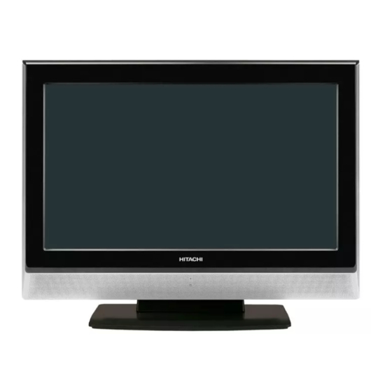
L26A01
L32A01
L32A01A
L32A01B
Data contained within this Service
manual is subject to alteration for
improvement.
Les données fournies dans le présent
manuel d'entretien peuvent faire l'objet
de modifications en vue de perfectionner
le produit.
Die in diesem Wartungshandbuch
enthaltenen Spezifikationen können sich
zwecks Verbesserungen ändern.
12. Block Diagrams
13. Troubleshooting Guide
Advertisement
Table of Contents


Need help?
Do you have a question about the L26A01 and is the answer not in the manual?
Questions and answers