
Related Manuals for Seiko Epson VG-4513CA

Summary of Contents for Seiko Epson VG-4513CA
- Page 1 INFORMATION Model : VG-4513CA DATE : 12th. Sep. 2013 SEIKO EPSON CORPORATION 8548 Nakaminowa, Minowa-machi, Kamiina-gun, Nagano-ken 399-4696 Japan OUT-13-0473 rev.2...
- Page 2 OUT-13-0473 rev.2 INTRODUCTION 1. The contents is subject to change without notice. Please exchange the specification sheets regarding the product’s warranty. 2. This sheet is not intended to guarantee or provide an approval of implementation of industrial patents. 3. We have prepared this sheet as carefully as possible. If you find it incomplete or unsatisfactory in any respect, We would welcome your comments.
-
Page 3: Specifications
1) This specifications apply to Crystal oscillator VG-4513CA for Alcatel-Lucent. 2) This product is compliant with RoHS Directive. 3) This Product supplied (and any technical information furnished, if any) by SEIKO EPSON CORPORATION. Corporation shall not be used for the development and manufacture of weapon of mass destruction or for other military purposes. - Page 4 OUT-13-0473 rev.2 [ 1 ] Absolute maximum ratings Parameter Symbol Value Unit Note Supply voltage -0.5 to +5.0 Input voltage -0.5 to V +0.5 Vc Terminal °C Storage temperature range * T_stg -55 to +125 Stored as bare product after unpacking. * Concerning the frequency change, please refer [8] Environmental and mechanical characteristics.
- Page 5 OUT-13-0473 rev.2 Output Frequency characteristics Value Parameter Symbol Unit Note Min. Typ. Max. ±100 122.880MHz-GGCT Pull range ±150 ×10 122.880MHz-GHCT Vc=1.65V±1.65V ±100 491.520MHz-GFCT ±50 122.880MHz-GGCT Absolute pull range *1 ±100 ×10 122.880MHz-GHCT Vc=1.65V±1.65V ±30 491.520MHz-GFCT Input resistance kΩ Vc terminal ( DC level ) Frequency tuning linearity Modulation band...
- Page 6 OUT-13-0473 rev.2...
- Page 7 OUT-13-0473 rev.2 [ 4 ] Terminal description FREQUENCY LOT No. Name Type Terminal description INPUT Vc terminal OE terminal / Active High GND terminal(*1) OUTPUT OUT1 Clock output terminal (Positive) OUTPUT OUT2 Clock output terminal(Inversion output of #4) (Negative) Vcc terminal * The metal part of the surface (metal cap) is connected to GND.
-
Page 8: [ 5 ] Electrical Characteristics
OUT-13-0473 rev.2 [ 5 ] Electrical characteristics Test condition is Vcc=3.3V, Vc=1.65V, at +25°C, unless otherwise noted. Value Note Parameter Symbol Unit Min. Start up time 0 sec at 90 % Vcc Current consumption Rise time (*1) 20 %Vcc 80 %Vcc Fall time (*1) 80 %Vcc 20 %Vcc... - Page 9 OUT-13-0473 rev.2 [ 6 ] Test circuit 1) To observe waveform and current 2) Condition (1) Oscilloscope • Bandwidth should be 5 times higher than DUT’s output frequency. • Probe ground should be placed closely from test point and lead length should be as short as possible. µ...
- Page 10 OUT-13-0473 rev.2 [ 7 ] Timing chart 1) Output wave form and measurement level OUT2 80 % of amplitude 20 % of amplitude OUT1 Vcc-2 V SYM = tw / t 2) Output Signal timing tosc Probe start 90%Vcc Probe timing 3) Vc control timing Please rise up the Vc voltage after the Vcc voltage rises up.
- Page 11 OUT-13-0473 rev.2 4) OE function and timing Oscillation circuit Output OE input level Oscillation “H” or OPEN Enable : Specified frequency is output Oscillation “L” Disable : OUT1->LOW, OUT2->HIGH Enable Disable OUT 2 OUT 1 *1 The time taken from OE=V to OUT=Disable.
- Page 12 OUT-13-0473 rev.2 [ 9 ] Dimensions and marking layout 1) Dimensions 7.0±0.2 1.6±0.2 C0.5 Terminal treatment : Au plating Unit : mm 5.08...
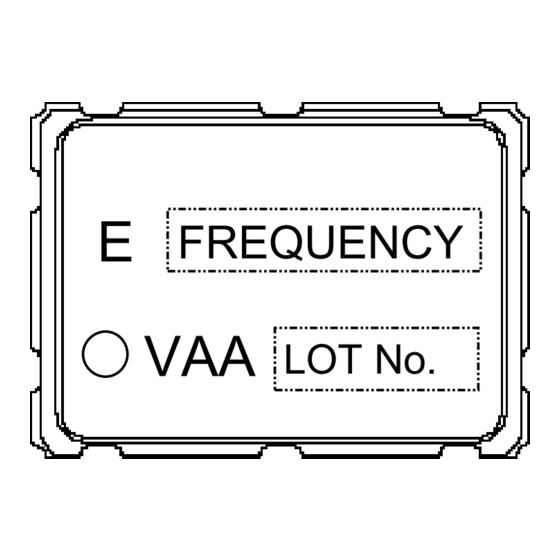
- Page 13 OUT-13-0473 rev.2 2) Marking layout E 122.880 Nominal frequency [MHz] Symbol mark VAA3ZMC Production Lot Number #1pin mark VCXO Product symbol PKG SIZE : 7.0x5.0mm * The above marking layout shows only marking contents and their approximate position, not actual font, size and exact position.
- Page 14 3) Vcc and GND pattern shall be as large as possible so that high frequency impedance shall be small. 4) SEIKO EPSON CORPORATION cannot recommend to put filtering element into power line so as to reduce noise. Oscillator might be unstable oscillation because high frequency impedance of power line become higher.
- Page 15 OUT-13-0473 rev.2 16) Recommendation reflow times are less than 2 times. When there was a soldering error, please do alteration with a soldering iron. In this case, the iron ahead is equal to or less than +350 °C and asks within 5 s. In case that this device is reflow soldered on the back side of your circuit board, please carefully verify the device is properly secured to prevent coming detached from card.
Need help?
Do you have a question about the VG-4513CA and is the answer not in the manual?
Questions and answers