Table of Contents
Advertisement
Quick Links
UM2525
User manual
Evaluation boards with STM32H747XI and STM32H757XI MCUs
Introduction
The
STM32H747I-EVAL
and
STM32H757I-EVAL
Evaluation boards (STM32H7x7I-EVAL) are high-end development platforms
for the
STM32H747XI
and
STM32H757XI
microcontrollers, respectively. They are based on the high-performance
®
®
‑M4 and Cortex
®
‑M7 cores. The STM32H7x7I-EVAL Evaluation boards provide access to all the STM32
Arm
Cortex
peripherals for user applications, and include an embedded STLINK-V3E debugger/programmer.
The full range of the STM32H7x7I-EVAL hardware features helps develop applications and evaluate all peripherals: USB OTG
HS and OTG FS, Ethernet, CAN FD, USART, audio DAC and ADC, digital microphone, SRAM, SDRAM, NOR flash memory,
™
®
twin Quad-SPI flash memory, microSD
3.0 card, 4" 480×800 TFT color LCD with MIPI DSI
interface and capacitive touch
panel, and cryptographic hardware accelerator (available only on
STM32H757XI
devices).
The expansion connectors provide an easy way to add specialized features, while ETM trace is supported through external
probes.
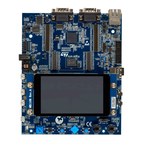
Figure 1.
STM32H7x7I-EVAL board (top view)
Picture is not contractual.
UM2525 - Rev 6 - April 2023
www.st.com
For further information contact your local STMicroelectronics sales office.
Advertisement
Table of Contents

Subscribe to Our Youtube Channel
Related Manuals for STI STM32H747I-EVAL


Summary of Contents for STI STM32H747I-EVAL
-
Page 1: Figure 1. Stm32H7X7I-Eval Board (Top View)
UM2525 User manual Evaluation boards with STM32H747XI and STM32H757XI MCUs Introduction STM32H747I-EVAL STM32H757I-EVAL Evaluation boards (STM32H7x7I-EVAL) are high-end development platforms for the STM32H747XI STM32H757XI microcontrollers, respectively. They are based on the high-performance ® ® ‑M4 and Cortex ® ‑M7 cores. The STM32H7x7I-EVAL Evaluation boards provide access to all the STM32 Cortex peripherals for user applications, and include an embedded STLINK-V3E debugger/programmer. -
Page 2: Features
UM2525 Features Features ‑M4 and Cortex ‑M7 microcontrollers with 2 Mbytes ® ® ® • STM32H747XIH6 and STM32H757XIH6 Arm Cortex of flash memory and 1 Mbyte of RAM in a TFBGA240+25 package ® • 4” 480×800 TFT color LCD with MIPI DSI interface and capacitive touch panel •... -
Page 3: Ordering Information
Table 1. Additional information is available from the datasheet and reference manual of the target STM32. Table 1. List of available products Order code Board reference Target STM32 Differentiating feature STM32H747I-EVAL STM32H747XIH6 • MB1166 • MB1246 STM32H757I-EVAL STM32H757XIH6 Cryptography •... -
Page 4: Development Environment
UM2525 Development environment Development environment System requirements ® ® ® • Multi‑OS support: Windows 10, Linux 64-bit, or macOS ® • USB Type-A or USB Type-C to Micro-B cable Note: ® macOS is a trademark of Apple Inc., registered in the U.S. and other countries and regions. ®... -
Page 5: Conventions
UM2525 Conventions Conventions Table 3 provides the conventions used for the ON and OFF settings in the present document. Table 3. ON/OFF convention Convention Definition Jumper JPx ON Jumper fitted Jumper JPx OFF Jumper not fitted Jumper JPx [1-2] Jumper fitted between Pin 1 and Pin 2 Solder bridge SBx ON SBx connections closed by 0 Ω... -
Page 6: Delivery Recommendations
UM2525 Delivery recommendations Delivery recommendations Some verifications are needed before using the Evaluation board for the first time, to make sure that no damage occurred during shipment and that no components are unplugged or lost. When the board is extracted from its plastic bag, check that no component remains in the bag. The main ™... -
Page 7: Stm32H7X7I-Eval Hardware Layout And Configuration
UM2525 STM32H7x7I-EVAL hardware layout and configuration STM32H7x7I-EVAL hardware layout and configuration The STM32H7x7I-EVAL Evaluation boards are designed around the STM32H7x7XIH6 (240+25-pin TFBGA package) microcontroller. Figure 2 shows the hardware block diagram for STM32H7x7XIH6 and illustrates the connection between the microcontroller and the peripherals (SDRAM, SRAM, NOR flash memory, twin Quad-SPI flash memory, color LCD, USB OTG connectors, USART, Ethernet, audio, CAN FD (FDCAN), ™... -
Page 8: Stm32H7X7I-Eval Evaluation Board Layout
UM2525 STM32H7x7I-EVAL Evaluation board layout STM32H7x7I-EVAL Evaluation board layout Figure 3. STM32H7x7I-EVAL Evaluation board (top side) Ethernet RJ45 I²C extension CAN FD connector connector USART1 (CN3) (CN2) (CN1) (CN4) Extension header Extension header (CN7) (CN7) STM32H7x7XI (U7) ETM TRACE (CN8) STDC14 Memory header (CN24) -
Page 9: Stm32H7X7I-Eval Evaluation Board Mechanical Drawing
UM2525 STM32H7x7I-EVAL Evaluation board mechanical drawing STM32H7x7I-EVAL Evaluation board mechanical drawing Figure 4 Table 4 show the mechanical dimensions for the MB1246 board with the 5.7” LCD daughterboard. Figure 4. STM32H7x7I-EVAL Evaluation board mechanical drawing Table 4. Mechanical dimensions Symbol Size(mm) Symbol Size(mm) -
Page 10: Embedded Stlink-V3E
UM2525 Embedded STLINK-V3E Embedded STLINK-V3E The STLINK-V3E programming and debugging tool is integrated on the STM32H7x7I-EVAL Evaluation board. The key STLINK-V3E features are the following: • Standalone probe with modular extensions • Self-powered through a USB connector (Micro-B) • USB 2.0 high-speed compatible interface •... -
Page 11: Table 5. Power Related Jumpers
UM2525 Power supply • 5 V DC power with 500 mA limitation from CN16, the USB OTG1_FS Micro-AB connector (USB 5 V power source on the silkscreen of JP10 (FS1)). • 5 V DC power from CN6 and CN7, the extension connectors for the daughterboard (the power source of the daughterboard on the silkscreen of JP10 (D5V)). - Page 12 UM2525 Power supply Jumper Description STlk To supply the STM32H7x7I-EVAL board through the daughterboard connectors (CN6 and CN7), set JP10 as shown below: STlk JP10 To supply the STM32H7x7I-EVAL board through the USB OTG1_FS (CN16), set JP10 as shown below: STlk To supply the STM32H7x7I-EVAL board through the USB OTG2_FS (CN18), set JP10 as shown below: STlk...
-
Page 13: Smps/Ldo Power Supply
UM2525 Clock source The LED LD9 lights up when the STM32H7x7I-EVAL Evaluation board is powered by the 5 V correctly. Note: To avoid the impact of USB PHY, Ethernet PHY and get precise results about current consumption on JP9, take into account the following cautions: Remove JP5 to avoid Ethernet PHY influence. -
Page 14: Reset Sources
UM2525 Reset sources Table 6. 25 MHz crystal X1 related solder bridges Solder Description bridge PH0 is connected to a 25 MHz crystal when SB39 is OFF (default setting). SB39 PH0 is connected to extension connector CN6 when SB39 is ON. In such case R15 must be removed to avoid disturbance due to the 25 MHz quartz. -
Page 15: Audio
UM2525 Audio Switch configuration Boot address option bytes Boot space ST programmed value: System bootloader at 0x0000 0000. Table 9. Boot related jumpers Jumper Description The Bootloader_BOOT0 is managed by pin 6 of connector CN2 (RS-232 DSR signal) when JP3 is ON. This configuration is used for bootloader application only. -
Page 16: Usb Otg1_Hs And Fs
UM2525 USB OTG1_HS and FS USB OTG1_HS and FS The STM32H7x7I-EVAL Evaluation board supports USB OTG1: • High-speed communication through a USB Micro-AB connector (CN14), USB high-speed PHY (U13) for high-speed function • Full-speed communication through another USB Micro-AB connector (CN16) The Evaluation board can be powered by these USB connectors (CN14 or CN16) at 5 V DC with 500 mA current limitation. -
Page 17: Microsd ™ Card
UM2525 microSD™ card Jumper Description USART1_TX is connected to the USART_RX of the STLINK-V3E controller when JP7 is set as shown below: USART1_RX is connected to RS-232 when JP8 is set as shown below (default setting): USART1_RX is connected to the USART_TX of the STLINK-V3E controller when JP8 is set as shown below: 6.12 ™... -
Page 18: Memories
UM2525 Memories A 50 M reference clock can be generated by PHY with 25 MHz crystal or with 25 M MCO from STM32H7x7XI. These two resources can be selected by setting jumper JP5 as shown in the table below. Table 14. Ethernet related jumpers Jumper Description... -
Page 19: Display And Input Devices
UM2525 Display and input devices 6.19 Display and input devices Four general-purpose-color LEDs (LD 1, 2, 3, and 4) are available as display devices. The 4-direction joystick (B4) with selection, wake-up (B2), and tamper/key button (B3) are available as input devices. -
Page 20: Mfx (Multifunction Expander)
UM2525 MFX (multifunction eXpander) 6.20 MFX (multifunction eXpander) MFX circuit on STM32H7x7I-EVAL Evaluation board acts as IO-expander. The communication interface between MFX and STM32H7x7XI is an I2C1 bus. The signals connected to MFX are listed in Table 17. MFX signals. Table 17. -
Page 21: Stm32H7X7I-Eval Connectors
UM2525 STM32H7x7I-EVAL connectors STM32H7x7I-EVAL connectors Ethernet RJ45 connector CN1 Figure 5. Ethernet RJ45 connector CN1 (front view) Table 18. RJ45 connector CN1 Pin number Description Pin number Description TxData+ TxData- RxData+ Shield Shield RxData- Shield Shield RS-232 connector CN2 Figure 6. RS-232 connector CN2 (front view) Table 19. -
Page 22: Can D-Type, 9-Pin Male Connector Cn3
UM2525 CAN D-type, 9-pin male connector CN3 CAN D-type, 9-pin male connector CN3 Figure 7. CAN D-type, 9-pin connector CN3 (front view) Table 20. CAN D-type 9-pin male connector CN3 Pin number Description Pin number Description 1, 4, 8, 9 CANH CANL 3, 5, 6... -
Page 23: Analog Input-Output Connector Cn5
UM2525 Analog input-output connector CN5 Analog input-output connector CN5 Figure 9. Analog input-output connector CN5 (top view) Table 22. Analog input-output connector CN5 Pin number Description Pin number Description analog input-output (PA0_C) Daughterboard extension connector CN6 and CN7 Two 60-pin male headers CN6 and CN7 can be used to connect a daughterboard or a standard wrapping board to the STM32H7x7I-EVAL Evaluation board. - Page 24 UM2525 Daughterboard extension connector CN6 and CN7 Pin Description Alternate function How to disconnect with function block on STM32H7x7I-EVAL board PB14 USART1_TX/USB_FS1_DM Open SB46, SB47 PB15 USART1_RX/USB_FS1_DP Open SB49, SB51 PB11 ULPI_D4 Remove R108 TRGIN Remove SB24 QSPI_BK1_NCS Open SB6, Remove R19 RMII_MDC/ PDM1_D1 Open SB38, Not to dial SW2 to the right QSPI_BK1_IO2...
-
Page 25: Table 24. Daughterboard Extension Connector Cn7
UM2525 Daughterboard extension connector CN6 and CN7 Table 24. Daughterboard extension connector CN7 How to disconnect with function block on STM32H7x7I-EVAL Pin Description Alternate function board PF10 GPIO_DSI_RST Remove R286, Disconnect CN15 PC15 OSC32_OUT Remove R17, Close SB4 PI14 PI13 PC13 KEY_TAMP_1/WKUP2 Remove R193... -
Page 26: Etm Trace Debugging Connector Cn8
UM2525 ETM trace debugging connector CN8 How to disconnect with function block on STM32H7x7I-EVAL Pin Description Alternate function board LED3 Remove R200 PJ13 PG12 RMII_TXD1 PJ14 PJ12 TRGOUT Remove SB25 GPIO_CAN_STBY Remove R4 PC10 SDIO_1_D2 Add R139 10Kohm PA14 JTCK-SWCLK Remove R59 PC11 SDIO_1_D3... -
Page 27: Jtag/Swd Connector Cn9
UM2525 JTAG/SWD connector CN9 Pin number Description Pin number Description TDI/PA15 RESET# TraceCLK/PE2 TraceD0/PE3 or SWO/PB3 TraceD1/PE4 or nTRST/PB4 TraceD2/PE5 TraceD3/PE6 JTAG/SWD connector CN9 Figure 11. JTAG/SWD debugging connector CN9 (top view) Table 26. JTAG/SWD debugging connector CN9 Pin number Description Pin number Description... -
Page 28: Power Connector Cn10
UM2525 Power connector CN10 Power connector CN10 The STM32H7x7I-EVAL Evaluation board can be powered from a DC 5 V power supply through the external power supply socket (CN10) shown in the figure below. The central pin of CN10 must be positive. Figure 12. -
Page 29: Table 28. Memory Connector Cn12
UM2525 Memory connector CN11 and CN12 Description Alternative function How to disconnect with function block on STM32H7x7I-EVAL board PD14 SDNWE PF14 PF11 SDNRAS PE11 PF15 PE14 PH10 A14/BA0 PH12 PD10 PD15 SDCLK Table 28. Memory connector CN12 How to disconnect with function block on Pin Description Alternative function STM32H7x7I-EVAL board... - Page 30 UM2525 Memory connector CN11 and CN12 How to disconnect with function block on Pin Description Alternative function STM32H7x7I-EVAL board PH13 SDCKE1 A21/SAI1_SCK_A/TRACED2 Open SB41, SB42 NWAIT A23/PDM1_CK1/ SAI1_MCLK_A /TRACECLK Open SB11, SB15, SB57 PH15 PH14 +3.3V UM2525 - Rev 6 page 30/49...
-
Page 31: Microsd™ Connector Cn13
UM2525 microSD™ connector CN13 7.11 ™ microSD connector CN13 ™ Figure 13. microSD connector (top view) ™ Table 29. microSD connector CN13 Pin number Description Pin number Description SD_DATA2 Vss/GND SD_DATA3 SD_DATA0 SD_CMD SD_DATA1 +2.9V_SD MicroSDcard_detect SD_CLK (MFX GPIO15) 7.12 USB OTG1_HS Micro-AB connector CN14 Figure 14. -
Page 32: Tft Lcd Connector Cn15
UM2525 TFT LCD connector CN15 Table 30. USB OTG1_HS Micro-AB connector CN14 Pin number Description Pin number Description 7.13 TFT LCD connector CN15 ® A TFT-color LCD with MIPI DSI interface board is mounted on CN15. Refer to Section 6.19 Display and input devices for details. -
Page 33: Audio Jack (Speaker) Cn19
UM2525 Audio jack (speaker) CN19 Table 32. USB OTG2_FS Micro-AB connector CN18 Pin number Description Pin number Description (PA9) ID (PA10) D- (PA11) D+ (PA12) 7.17 Audio jack (speaker) CN19 A 3.5 mm stereo audio jack CN19 for speaker-out is available on the STM32H7x7I-EVAL Evaluation board to support an external speaker. -
Page 34: Stdc14 Debugging Connector Cn24
UM2525 STDC14 debugging connector CN24 7.21 STDC14 debugging connector CN24 Figure 18. STDC14 debugging connector CN24 (top view) Table 34. STDC14 debugging connector CN24 Pin number Description Pin number Description +3.3V SWDIO-TMS/PA13 SWCLK-TCK/PA14 SWO-TDO/PB3 TDI/PA15 GNDDetect RESET# VCP_USART_RX/PB14 VCP_USART_TX/PB15 7.22 MEMS microphone coupon connectors CN25 and CN26 Figure 19. -
Page 35: Stm32H7X7I-Eval I/O Assignment
UM2525 STM32H7x7I-EVAL I/O assignment STM32H7x7I-EVAL I/O assignment Table 36. STM32H7x7I-EVAL I/O assignment Pin number Pin name Default function Alternate function PA0-WKUP KEY_WKUP0 RMII_REF_CLK RMII_MDIO ULPI_D0 EXT_RESET ULPI_CK GPIO_LCD_BACKLIGHT_CTRL RMII_CRS_DV MCO1 USB_FS2_VBUS PA10 USB_FS2_ID PA11 USB_FS2_DM FDCAN_1_RXFD PA12 USB_FS2_DP FDCAN_1_TXFD PA13 JTMS-SWDIO PA14 JTCK-SWCLK... - Page 36 UM2525 STM32H7x7I-EVAL I/O assignment Pin number Pin name Default function Alternate function SDIO_1_D0DIR SDIO_1_D123DIR SDIO_1_D0 SDIO_1_D1 PC10 SDIO_1_D2 PC11 SDIO_1_D3 PC12 SDIO_1_CK PC13-ANTI_TAMP KEY_TAMP_1/WKUP2 PC14-OSC32_IN OSC32_IN PC15-OSC32_OUT OSC32_OUT FMC_D2 FMC_D3 SDIO_1_CMD GPIO_CAN_STANDBY FMC_NOE FMC_NWE FMC_NWAIT FMC_NE1 FMC_D13 FMC_D14 PD10 FMC_D15 PD11 FMC_A16 PD12...
- Page 37 UM2525 STM32H7x7I-EVAL I/O assignment Pin number Pin name Default function Alternate function PE15 FMC_D12 FMC_A0 FMC_A1 FMC_A2 FMC_A3 FMC_A4 FMC_A5 QSPI_BK1_IO3 QSPI_BK1_IO2 QSPI_BK1_IO0 QSPI_BK1_IO1 PF10 GPIO_DSI_RST PF11 SDR_SDNRAS PF12 FMC_A6 PF13 FMC_A7 PF14 FMC_A8 PF15 FMC_A9 FMC_A10 FMC_A11 FMC_A12 FMC_A13 FMC_A14 / SDR_BA0 FMC_A15 / SDR_BA1 QSPI_BK1_NCS...
- Page 38 UM2525 STM32H7x7I-EVAL I/O assignment Pin number Pin name Default function Alternate function FMC_D16 FMC_D17 PH10 FMC_D18 PH11 FMC_D19 PH12 FMC_D20 PH13 FMC_D21 PH14 FMC_D22 PH15 FMC_D23 FMC_D24 FMC_D25 FMC_D26 FMC_D27 FMC_NBL2 FMC_NBL3 FMC_D28 FMC_D29 PI8- ANTI TAMP2 GPIO_EXPANDER_INT FMC_D30 PI10 FMC_D31 PI11 ULPI_DIR...
- Page 39 UM2525 STM32H7x7I-EVAL I/O assignment Pin number Pin name Default function Alternate function LED1 LED2 LED3 LED4 PA0_C Potentiometer PA1_C PC2_C PC3_C UM2525 - Rev 6 page 39/49...
-
Page 40: Stm32H747I-Eval And Stm32H757I-Eval Product Information
UM2525 STM32H747I-EVAL and STM32H757I-EVAL product information STM32H747I-EVAL and STM32H757I-EVAL product information Product marking The stickers located on the top or bottom side of all PCBs provide product information: • First sticker: product order code and product identification, generally placed on the main board featuring the target device. -
Page 41: Stm32H7X7I-Eval Product History
UM2525 STM32H7x7I-EVAL product history STM32H7x7I-EVAL product history Table 37. Product history Order Product Product details Product change description Product limitations code identification MCU: • STM32H757XIH6 silicon revision "V" MCU errata sheet: • STM32H745/747xI/G and STM32H755/757xI device limitations (ES0445) 32H757I-EVAL/ Initial revision No limitation Boards: •... -
Page 42: Board Revision History
UM2525 Board revision history Board revision history Table 38. Board revision history Board reference Board variant and revision Board change description Board limitations MB1166 (LCD board) Default-A08 Initial revision No limitation H747-E02 Initial revision No limitation H757-E02 • Memory IS42S32800G-6BLI MB1246 (main board) replaced by IS42S32800J-6BLI H757-E03... -
Page 43: Federal Communications Commission (Fcc) And Ised Canada Compliance
UM2525 Federal Communications Commission (FCC) and ISED Canada Compliance Statements Federal Communications Commission (FCC) and ISED Canada Compliance Statements 10.1 FCC Compliance Statement Part 15.19 This device complies with Part 15 of the FCC Rules. Operation is subject to the following two conditions: (1) this device may not cause harmful interference, and (2) this device must accept any interference received, including interference that may cause undesired operation. -
Page 44: Revision History
Removed schematics. Removed obsolete order code in Section 2 Ordering information. Replaced Board revision history and limitations with Section 9 STM32H747I-EVAL and STM32H757I-EVAL product information. 25-Apr-2023 Updated Section 10 Federal Communications Commission (FCC) and ISED Canada Compliance Statements. -
Page 45: Table Of Contents
UM2525 Contents Contents Features................2 Ordering information . - Page 46 STM32H7x7I-EVAL I/O assignment ..........35 STM32H747I-EVAL and STM32H757I-EVAL product information....40 Product marking .
-
Page 47: List Of Tables
UM2525 List of tables List of tables Table 1. List of available products............. . . 3 Table 2. -
Page 48: List Of Figures
UM2525 List of figures List of figures Figure 1. STM32H7x7I-EVAL board (top view) ........... . . 1 Figure 2. - Page 49 UM2525 IMPORTANT NOTICE – READ CAREFULLY STMicroelectronics NV and its subsidiaries (“ST”) reserve the right to make changes, corrections, enhancements, modifications, and improvements to ST products and/or to this document at any time without notice. Purchasers should obtain the latest relevant information on ST products before placing orders. ST products are sold pursuant to ST’s terms and conditions of sale in place at the time of order acknowledgment.
Need help?
Do you have a question about the STM32H747I-EVAL and is the answer not in the manual?
Questions and answers