Table of Contents
Advertisement
Quick Links
Copyright © 2003 Daniels Electronics Ltd. All rights reserved. No part of this publication may be reproduced, stored
in a retrieval system or transmitted in any form or by any means, electronic, mechanical, photocopying, recording or
otherwise, without the prior written consent of Daniels Electronics Ltd.
DE™ is a registered trademark of Daniels Electronic Ltd. registered in the U.S. Patent and Trademark Office.
Revision Date: Aug 2003
Revision:
1-1-0
Document No.: IM10-VR3H040-AB
MT-3 RADIO SYSTEMS
VHF ENHANCED
EXTRA WIDEBAND
RECEIVER
INSTRUCTION MANUAL
VR-3H
Covers model: VR-3H035-SWA, VR-3H045-SWA
Converted for 50 kHz Channel spacing
DANIELS
ELECTRONICS LTD.
29 - 50 MHz
TM
Daniels Electronics Ltd.
Victoria, BC
PRINTED IN CANADA
Advertisement
Table of Contents

Summary of Contents for Daniels Electronics VR-3H
- Page 1 Converted for 50 kHz Channel spacing Copyright © 2003 Daniels Electronics Ltd. All rights reserved. No part of this publication may be reproduced, stored in a retrieval system or transmitted in any form or by any means, electronic, mechanical, photocopying, recording or otherwise, without the prior written consent of Daniels Electronics Ltd.
- Page 2 DOCUMENT CONTROL: This document has been produced, verified and controlled in accordance with Daniels Electronics’ Quality Management System requirements. Please report any errors or problems to Daniels Electronics’ Customer Service Department. NOTE: The user's authority to operate this equipment could be revoked through any changes or modifications not expressly approved by Daniels Electronics Ltd.
-
Page 3: Table Of Contents
TABLE OF CONTENTS Page GENERAL......................... 1-1 1.1 Introduction......................1-1 1.2 VR-3H040 Extra Wideband Receiver Family Models ........1-1 1.3 Manual Organization ..................1-2 1.4 Performance Specifications ................1-3 1.4.1 General......................1-3 1.4.2 Enhanced Front End Performance Specifications ......... 1-5 1.4.3 Enhanced Synthesizer Performance Specifications........1-5 1.4.4 Physical Specifications .................. - Page 4 3.2.4 RF Amplifier....................3-9 3.2.5 Image Rejection Filter ................... 3-9 3.2.6 Local Oscillator Filter..................3-9 3.2.7 Double Balanced Mixer ................. 3-9 3.3 Enhanced Synthesizer ..................3-10 3.3.1 Internal Power and Control (Digital Board) ..........3-10 3.3.2 Common Analog Board Circuitry..............3-10 3.3.3 29 - 71.4 MHz Analog Board Circuitry............
- Page 5 ILLUSTRATIONS AND SCHEMATIC DRAWINGS ..........6-1 6.1 21.4 MHz IF/Audio Board Component Layout (Bottom) – Extra Wideband ... 6-1 6.2 21.4 MHz IF/Audio Board Component Layout (Top) – Extra Wideband..6-2 6.3 21.4 MHz IF/Audio Board Schematic Diagram – Extra Wideband ....6-3 6.4 21.1 MHz FM IF Buffer Component Layout ............
- Page 6 This Page Intentionally Left Blank DANIELS ELECTRONICS LTD. IM10-VR3H040-AB VHF Enhanced Extra Wideband Receiver Instruction Manual...
-
Page 7: General
GENERAL Introduction The VR-3H040 Enhanced Extra Wideband Receiver family provides high performance synthesized FM reception in 50 kHz channels in one of two frequency bands: 29 to 38 MHz or 38 to 50 MHz. A modular design allows each of the receiver's three internal modules; 21.4 MHz FM IF/Audio Main Board, FE3H Enhanced Front End, and OS-3H Synthesizer to be individually assembled and tested. -
Page 8: Manual Organization
Enhanced Synthesizer Module. The synthesizer module provides the low noise first local oscillator signal to the FE3H Front End module. VR-3H 29 - 50 MHz Channel Designation Tables: This manual provides tabular frequency / channel number assignment. -
Page 9: Performance Specifications
Performance Specifications 1.4.1 General Type: MT-3 Series Synthesized Receiver. Family: VR-3H040 Converted for 50 kHz Channel spacing Compatibility: MT-3 Series Radio Systems Frequency Range: 29 to 38 MHz or 38 to 50 MHz. System Impedance: 50 Ω (Type N connector). Frequency Generation: Synthesizer Module (Internal). - Page 10 Audio Output: 600 Ω balanced or unbalanced line output; De-emphasis output, +3 dBm maximum level; Flat response output, +3 dBm maximum level; Audio Distortion: Less than 3.0% (typical < 2%) THD at +25°C; less than 3.5% THD, -30°C to +60°C. De-emphasized Audio Response: +1, -2 dB;...
-
Page 11: Enhanced Front End Performance Specifications
1.4.2 Enhanced Front End Performance Specifications Frequency Range: 29.0 MHz - 38.5 MHz (FE3H035) 37.5 MHz - 50.0 MHz (FE3H045) IF Frequency: 21.4 MHz 3 dB Bandwidth: > 5 MHz (Preselector Filter) Conversion Gain: 12.5 dB Third Order Intercept Point: >... -
Page 12: Physical Specifications
1.4.4 Physical Specifications Physical Dimensions: Width: Height: Depth: 7.1 cm (2.8 in) 12.8 cm (5.05 in) 19 cm (7.5 in) Module Weight: 1.0 kg (2.2 lbs) Corrosion Prevention: Anodized aluminum construction. Stainless steel hardware. Selectively conformal coated glass epoxy 2 and 4 layer printed circuit boards. -
Page 13: System Overview
SYSTEM OVERVIEW Receiver Operation A VR-3H040 Receiver family is constructed using three primary modules; the FE3H Front-End module, the MT-3 Receiver FM IF/Audio Main Board and the OSR-3H061 local oscillator synthesizer (refer to section 3.3, VR-3H040 Family Enhanced Receiver Block Diagram). Two Front-End modules, FE3H035 and FE3H045 provide frequency coverage from 29 - 38 MHz and 38 - 50 MHz respectively. -
Page 14: Frequency Selection
Frequency Selection Receiver channel selection is achieved by setting a decimal number on four BCD frequency select switches, FSW1 through FSW4. These rotary switches are located on the FM IF/Audio Main Board and are made accessible by removing the outer receiver cover. The switch settings are scanned by the synthesizer module when the receiver is first powered up, and the desired local oscillator frequency is generated. -
Page 15: Receiver Assembly And Adjustment
Receiver Assembly and Adjustment All modules and the front panel are mounted on the Receiver Main Board which then forms a single assembly. The FE3H Front End is attached with two front panel screws and one screw through the rear F connector. Removal is required to access the Synthesizer for tuning. An enclosure is formed by an extruded aluminum shell that slides over the Receiver Main Board as illustrated in section 2.8). -
Page 16: Frequency Change
2.3.2 Frequency Change The receiver is initially aligned at the factory for the frequency stamped on the 'Factory Set Operating Frequency' label (see section 3.1). This label should list the frequency at which the last complete receiver alignment was performed. For a small frequency change, a simple channel change (see section 2.2) may be all that is required. -
Page 17: Minor Frequency Change
2.3.3 Minor Frequency Change Changes less than ± 0.5 MHz (29 - 38 MHz) or ± 1 MHz (38 - 50 MHz) from a previously tuned working receive frequency will generally not require any adjustment. Change the channel frequency select switches (Section 2.2) and inject a standard signal at the new channel frequency. -
Page 18: Mhz If/Audio Main Board
The FE3H040 Enhanced Front End is a highly integrated, frequency selective, down converter used in Daniels Electronics standard MT-3 Low Band VHF FM receiver product line. The FE3H040 Front End connects to the 21.4 MHz IF / Audio Main Board and the enhanced Synthesizer to form a complete receiver. -
Page 19: Enhanced Synthesizer
Enhanced Synthesizer The OS-3A/H Synthesizer is a compact, fully shielded and environmentally rugged frequency synthesis module that is the nucleus of every MT-3 synthesized Receiver and Transmitter radio module. The OS-3A/H generates a high stability, low distortion radio frequency signal in one of several frequency bands, including 29 - 50 MHz. -
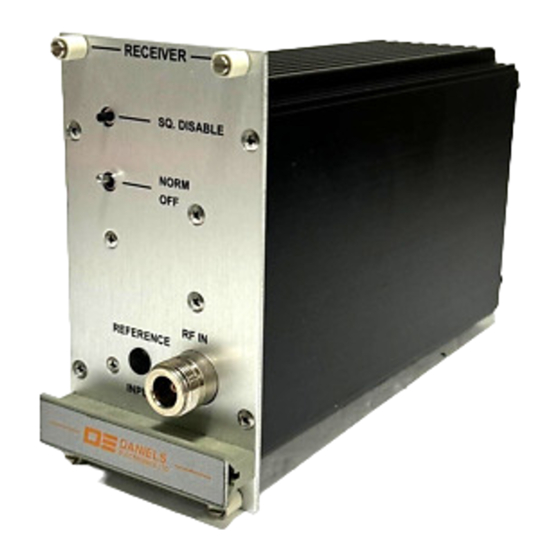
Page 20: Receiver Front Panel Illustration
Receiver Front Panel Illustration RECE VER FACTORY SET FREQUENCY (MHz) 45.120 OPERATING FREQUENCY SQUELCH DISABLE SQ . DI SABLE ON / OFF SWITCH RF N REFERENCE TYPE N RF SMA REFERENCE INPUT JACK INPUT JACK INPUT ORANGE TEXT MADE IN CANADA VR-3H045-SW MADE IN CANADA RECEIVER... -
Page 21: Receiver Case - Exploded View
MT-3 Receiver Case - Exploded View RECEIVER FRONT PANEL ASSEMBLY RECEIVER 14 HP CASE Instructions 1. Remove the four screws (D) on the side of the Receiver Case. 2. Remove the four Front Panel screws (A). RF AMPLIFIER ASSEMBLY 3. Remove the Receiver Case. 4. -
Page 22: Vr-3H040 Family Enhanced Receiver Block Diagram
TP1 TP3 TP2 RECEIVER MAIN POWER VR-3H040 Family Enhanced Receiver Block Diagram (FRONT PANEL) +9.5 VDC +9.5 VDC SUPPLY +6.0 VDC POWER SUPPLY 4.70 +9.5 VDC SUPPLY U1, U12, U13 +4.75 VDC -6.0 VDC 3.70 +6.0 VDC OUTPUT 2.70 ENHANCED RF AMPLIFIER FRONT END FRONT PANEL RF INPUT (TYPE N CONNECTOR) 21.4 MHz... -
Page 23: Theory Of Operation
THEORY OF OPERATION Detailed circuit analysis and signal flow description for each of the three electronic modules; Main Board, Enhanced Front End, and Synthesizer are provided in the subsections below. Refer to Section 2, System Overview, of this manual for a description of the overall receiver operation, and the receiver block diagram. -
Page 24: First If Amplifier
3.1.4 First IF Amplifier MOSFET Q1 provides linear 21.4 MHz IF amplification, while crystal filters XF1 through XF4 provide the optimum bandpass characteristics for good selectivity and low distortion. Potentiometer R13 is used to bias Q1 to an operating point drain current of 7.5 mA. The 21.4 MHz IF amplifier provides an overall gain of approximately 14 dB, including crystal filter losses. -
Page 25: Audio Processing
Graph of the RSSI Output Voltage versus RF Signal Level. 4.70 3.70 2.70 1.70 0.70 -120.0 -100.0 -80.0 -60.0 -40.0 RF SIGNAL LEVEL (dBm) MT3RXM4 Note: Standard input signal used (1kHz tone, 3 kHz deviation). 3.1.7 Audio Processing Recovered audio from pin 9 of U2 supplies both audio and squelch circuitry. Operational amplifier U18A is AC coupled to the recovered audio line providing low pass filtering with a cutoff frequency of approximately 8 kHz, together with amplification of the recovered audio signal. -
Page 26: Post Discriminator Filtering
Operational amplifier U19A is AC coupled to the recovered audio line providing the standard 6 dB per octave de-emphasis response from 300 Hz to 3 kHz. The de-emphasis audio output can be routed, via jumpers JU13, JU14 and JU15, through a voice band filter and/or connected directly through the audio squelch gate U7. -
Page 27: Squelch Circuitry
Operational amplifiers U5 and U6 form a 6 pole voice band high pass filter that is used to remove modulation components below 300 Hz. Enabled by the installation of jumpers JU8 and JU9, the voice band high pass filter provides an output that can be routed through either the flat or de-emphasis audio paths via jumpers JU12 or JU15. -
Page 28: Cor Outputs
This provides a controlled amount of squelch hysteresis that prevents oscillating action of the squelch comparator circuitry. The amount of squelch hysteresis is normally factory set for 6 dB centered about the squelch threshold point. The squelch threshold setting is normally established as being the point of receiver 12 dB SINAD. -
Page 29: Channel Selection
The other three COR outputs are all affected by the receiver's mute line, consequently, they only become active when the Receiver is unsquelched. • MOSFET Q5 provides an open drain output capable of sinking up to 2 amps when active (unsquelched receiver) through main connector pins B12 / Z12. Jumpers JU26 and JU27 allow internal pull-up to either +6.0 Vdc or +9.5 Vdc respectively. -
Page 30: Enhanced Front End
Enhanced Front End 3.2.1 General The Enhanced Front End amplifies and down converts the RF signal to the IF frequency of 21.4 MHz. The FE3H035 and FE3H045 Front Ends use high side injection. The Enhanced Front End consists of the following: •... -
Page 31: Local Oscillator Filter
3.2.4 RF Amplifier The output from the preselector filter is coupled through DC blocking capacitor C8 to the base of RF amplifier Q2. The RF amplifier stage is supplied by the regulated +9.5 Vdc line and typically draws 60 mA of collector current. It provides a high third order intercept point and low noise figure. -
Page 32: Internal Power And Control (Digital Board)
Enhanced Synthesizer 3.3.1 Internal Power and Control (Digital Board) Refer to "OS(R/T)-3(A/H) Digital Board Schematic Diagram" in section 6.13 of this manual. The synthesizer operates from a +9.5 Vdc power source applied to connector pin P1-2. Total current draw is approximately 160 mA for FM synthesizers and 65 mA for AM synthesizers. POWER DOWN control line P2-4 controls the +5.0 Vdc microcontroller regulator U2 through power MOSFET switch U1. - Page 33 The internal 9.6 MHz TCXO provides better than ±1 ppm frequency stability from -30°C to +60°C (-40°C to +60°C optional). Fine frequency adjustment is made through frequency control potentiometer RV1, which is accessible through the synthesizer top cover. The 9.6 MHz reference source is divided down to establish a channel selection step size of 5.0/6.25, 12.5, or 25.0 kHz depending on the particular synthesizer model type.
-
Page 34: 71.4 Mhz Analog Board Circuitry
3.3.3 29 - 71.4 MHz Analog Board Circuitry Refer to the "OS(R/T)-3H 29 - 71.4 MHz Analog Board Schematic Diagram" in section 6. Field effect transistor Q5 forms part of the negative resistance VHF amplifier oscillator that is tuned on-frequency by the combination of resonator L5 and the total capacitive reactance presented across L5 through capacitors C62, C63, C64, C23 (Select), variable capacitor C24 and varactor diodes D1 and D2. -
Page 35: Synthesizer Digital Circuitry (Digital Board)
3.3.4 Synthesizer Digital Circuitry (Digital Board) Microcontroller U4 generates control signals utilized within the synthesizer module. communicates with synthesizer IC U10, monitors the synthesizer lock detect, manages PTT input and output and determines the operating frequency by reading channel number information from either the four rotary Binary Coded Decimal (BCD) switches mounted on the main Transmitter and Receiver PCB, or by reading four externally driven CHANNEL SELECT lines. -
Page 36: Synthesizer Base And Frequency Increment Table
In transmitters, the synthesizer operating frequency is the transmitter operating frequency; however, for receivers, an IF Offset correction factor must be added to or subtracted from the synthesizer operating frequency in order to determine the actual receive frequency. For VHF and UHF Receivers, the IF Offset correction factor is 21.4 MHz, while for 800 and 900 MHz Receivers it is 45 MHz. -
Page 37: Receiver Alignment
RECEIVER ALIGNMENT General Receiver alignment is simplified by using an M-3 subrack, SM-3 system monitor, and RF extender card/cable to provide receiver power and signal interconnection. Alternatively, +9.5 Vdc may be applied directly to a receiver module through positive connection to pins B6 / Z6, and negative connection to pins B30 / Z30 / B32 / Z32. -
Page 38: Printed Circuit Board Numbering Convention
PCB number 43-912010 indicates circuit board version 1.0; • PCB number 50002-02 indicates circuit board version 2.0. All PCB's manufactured by Daniels Electronics are identified by one of the above conventions. Recommended Test Equipment Alignment of the receiver requires the following test equipment or its equivalent. -
Page 39: Synthesizer Os-3, Os-3H)
Synthesizer OS-3, OS-3H) For LOW BAND units (OSR-3H061 synthesizer): • Change the select jumpers, JU2, 3, 4 (See Table below). LOW BAND JUMPER TABLE – Use only with Analog Board PCB 50038-03 (Version 03). – Table to be used only as a guideline in choosing correct setting. Freq. - Page 40 Continue to decrease the jumper position one "bit" at a time until the synthesizer regains lock with TP4 adjusted (C24) for +2.3 Vdc. If the tuning voltage remains lower than +2.3 Vdc, increase the jumper setting by 1 "bit" position and re-adjust C24 in an attempt to achieve +2.3 Vdc at TP4.
-
Page 41: Front End Tuning
Front End Tuning • Attach the front-end assembly to the main board and solder the red wire to the 9.5V line (J6-2). • Use a spectrum analyzer with Tracking Generator. Connect the generator O/P of the spectrum analyzer to the RF I/P of the front end. Connect the IF O/P of the front end to the analyzer I/P. -
Page 42: Main Board Tuning
Main Board Tuning 4.7.1 IF Amplifier Bias Current Adjustment Monitor test point TP5 and adjust MOSFET bias potentiometer R13 until a DC level of +8.75 Vdc is achieved. This corresponds to an IF amplifier drain current of 7.5 mA, and prepares the IF amplifier for following alignment steps. -
Page 43: Distortion And Sensitivity
4.7.4 Distortion and Sensitivity • Adjust L2, C17, C27, and L5 to get lowest distortion. Experiment with L2 and C17 to get the best trade-off resulting in lowest distortion. Ensure distortion is < 3.0%. Expect ~ 1.5% or less for most units. •... -
Page 44: Squelch Window
4.7.6 Squelch Window • Generally, the squelch hysterisis is set to a window of 6dB centered around the 12dB SINAD sensitivity. • Set the RF Gen level to 3dB above the sensitivity. Turn pot R88 CW until the Rx’s audio O/P turns off. Slowly turn R88 CCW until the signal just comes on and stays on. •... -
Page 45: Receiver Configuration And Test Points
RECEIVER CONFIGURATION AND TEST POINTS 21.4 MHz IF / Audio Main Board Factory Settings 5.1.1 The 21.4 MHz IF/Audio Main Board Configuration: • Audio de-emphasis response enabled (JU14). • Flat audio response enabled (JU11). • 600 Ω balanced de-emphasis high level drive (JU17, JU18, JU22 and JU35 [Narrow Band Only]). -
Page 46: Test Points
• Jumper JU26: not installed +6.0 Vdc COR pull-up • Jumper JU27: not installed +9.5 Vdc COR pull-up • Jumper JU28: not installed Opto-isolated COR enable • Jumper JU29: not installed Relay COR enable • Jumper JU30: installed Noise based squelch select •... -
Page 47: Power Supplies
5.1.4 Power Supplies A check of all DC power supply levels is recommended before receiver alignment is performed. All supply and reference voltages are fixed with no provision made for adjustment. The following test points and their respective levels apply: Note that total receiver current should be less than approximately 100 mA for a synthesized unit and 45 mA for a crystal controlled unit. -
Page 48: Mhz If / Audio Board Interconnect Pin Definitions
5.1.5 21.4 MHz IF / Audio Board Interconnect Pin Definitions The IF / Audio Main Board employs a 48 pin Eurostandard connector for interfacing to all transmitter power, audio, and control functions. The following are the IF / Audio Main Board back plane connections to the M-3 Motherboard. -
Page 49: Os(R/T)-3(A/H) Synthesizer Factory Configuration
OS(R/T)-3(A/H) Synthesizer Factory Configuration The OS(R/T)-3(A/H) Synthesizer is factory configured as follows: • Internal 9.6 MHz reference selected. • VCO modulation (via audio processor) enabled (OST TX versions only) The corresponding internal synthesizer jumper settings are: Digital Board • Jumper JU2 not installed 9.6 MHz internal frequency reference selected •... -
Page 50: Synthesizer Test Points
5.3.2 Synthesizer Test Points Analog Board Component Layout (Top) Common to all synthesizer family members. +8.0 ±0.3 Vdc. U6 positive regulator output. +5.0 ±0.1 Vdc. U7 positive regulator output. +5.0 ±0.1 Vdc. U8 positive regulator output (always on). PLL error voltage. Normal range is +0.5 to +4.5 Vdc (depending on frequency). - Page 51 ILLUSTRATIONS AND SCHEMATIC DIAGRAMS 21.4 MHz FM IF / Audio Board Component Layout (Top) - Extra Wideband FRONT END CONNECTION C126 +9.5V 100µF 100µF Installed 13.8V 1 ROW x 6 PIN PCB HOLDER (FASTENED TO FRONT PANEL) 1 ROW x12 PIN 1 ROW x 9 PIN 150mH C116...
- Page 52 21.4 MHz FM IF / Audio Board Component Layout (Bottom) - Extra Wideband MBZD 5233 C128 21.4 10nF C140 475R 10k0 Freq. PRESS NUT 2.2µF BAS16 JU39 10k0 45.0 STANDOFF R107 STANDOFF JU33 R103 10k0 BAS16 BC817 BAS16 C125 RFC 30 10k0 narrow 12.5...
- Page 53 21.4 MHz FM IF / Audio Board Schematic Diagram - Extra Wideband Page 1 of 2 TO ALL - 6.0 VDC SUPPLY POINTS TO ALL +6.0 V CCTS TO ALL +9.5 V CCTS TO ALL +4.75 VDC SUPPLY POINTS BYD17 RECEIVER JU36 +9.5V...
- Page 54 21.4 MHz FM IF / Audio Board Schematic Diagram - Extra Wideband Page 2 of 2 JU44 JU43 JU25 187k RFC 12 DISCRIMINATOR O/P +9.5V B-14 7 POLE VOICE BAND HIGH PASS FILTER (Fc = 300 Hz) 33pF +9.5V (BUFFERED) U18B 22k6 C132...
-
Page 55: Mhz Fm If Buffer Component Layout
21.4 M H z F M I F Bu ffer C omp on en t L a you t 680nH 10nF 68pF 49R9 680nH 56pF 332R 82pF 121R 820nH 121R 1.0µH 100nF RX214M5 21.4 M H z F M I F Bu ffer Sch ema tic Dia gra m 9.5V 121R 121R... -
Page 56: Enhanced Front End Block Diagram
Enhanced Front End Block Diagram BANDPASS IMAGE REJECTION DOUBLE FILTER FILTER BALANCED MIXER RF IN IF OUT 21.4 MHz CONVERSION IL = 2 dB 16 dB IL = 1.5 dB 12.5 dB GAIN LOSS = 0 dB 3 dB BW > 5 MHz Fc = 61 MHz LOCAL OSCILLATOR FILTER... -
Page 57: Enhanced Front End Schematic Diagram - Extra Wideband
Enhanced Front End Schematic Diagram - Extra Wideband 10.0µH +9.5 VDC RF AMPLIFIER 4.7µF 100nF 10nF 1K00 332R0 IMAGE REJECTION FILTER LOW PASS FILTER BC807-25 220nH 270nH 220nH 30R1 100nF 10nF 1.0nF 10nF 2.2µH 47pF 100pF 100pF 47pF 3K01 BAND PASS FILTER 10nF 10nF 1K82... - Page 58 This Page Intentionally Left Blank DANIELS ELECTRONICS LTD. IM10-VR3H040-AB VHF Enhanced Extra Wideband Receiver Instruction Manual...
-
Page 59: Enhanced Front End Component Layout - Extra Wideband
6.10 Enhanced Front End Component Layout - Extra Wideband 0R00 100nF 5K11 5K11 47pF 4R75 4.7µF NE46134 10nF 100nF 1K82 150nH 180nH 150nH 49R9 100nF 49R9 220pF 10nF AD831AD 220nH 100nF 100pF 47pF 4.7µF 10nF 121R 121R 100nF 270nH 2.2µH 3K01 10nF 10nF... - Page 60 6.11 Synthesizer Analog Board Component Layout Bottom) - Extra Wideband 1.0µF 10µH 10µH COMPONENT LOCATION TABLE DES LC SD DES LC SD DES LC SD LC SD DES LC SD C41 C5 F2 B B2 T F3 T C42 E4 E2 B A4 T D1 T...
- Page 61 6.12 Synthesizer Analog Board Component Layout (Top) - Extra Wideband TRANSMITTER RECEIVER TX 29 - 40 MHz TX 39 - 50 MHz RX 50.4 - 71.4 MHz DESIG. OST - 3H035 OST - 3H045 OSR - 3H061 Remove seven M2.0 MMBV609L 150 pF 68 pF...
- Page 62 +8VA 6.13 Synthesizer Analog Board Schematic Diagram - Extra Wideband SI9945DY 10R0 BYD17J AGND MODULATION INPUT +8VA TO ALL +8VA SUPPLY POINTS 100uF 100uF +8VA +8VA 10uH OUTPUT C48 LEADS SHORTED AGND AGND + C12 1.0nF FOR TX MODELS 1.0nF 11K8 4.7uF ONLY.
- Page 63 6.14 Synthesizer Digital Board Schematic Diagram - Extra Wideband +5VD PRIORITY COR +5VD +5VD P1-12B TO ALL +5 VDC SUPPLY POINTS +5VD 10.0uH P1-2 SI9933DY 27K4 68HC811E2 CHAN SEL3 (I/P) P1-20 27K4 DGND 27K4 + C3 LP2951 27K4 +5VD BC817 27K4 100nF 47uF...
- Page 64 6.15 Synthesizer Digital Board Component Layout (Bottom) - Extra Wideband 100nF BC817 4.7uF MC33064 27k4 6k81 27k4 P1 1ROW x 12P 1ROW x 9P 22pF 8.0Mhz 10M0 68HC11E2 22pF OPL550 27k4 27k4 27k4 OP140A 10k0 BAS16 BC817 OP140A 1ROW x 6P 10k0 OP140A 47uF...
- Page 65 6.16 Synthesizer Digital Board Component Layout (Top) - Extra Wideband BC817 27k4 27k4 27k4 27K4 27k4 27k4 27k4 27k4 27k4 27k4 27k4 27k4 BC817 27k4 27k4 27k4 27k4 27k4 BC817 27k4 27k4 27k4 27k4 10k0 100nF R 33 332R BC817 BC817 100nF R 17...
- Page 66 This Page Intentionally Left Blank DANIELS ELECTRONICS LTD. 6-16 IM10-VR3H040-AB VHF Enhanced Extra Wideband Receiver Instruction Manual...
-
Page 67: Parts Lists
PARTS LISTS Electrical Parts Lists 7.1.1 21.4 MHz IF/Audio Main Board Ref. Desg. Description Part Numbers VT-3H035-SWA VT-3H045-SWA CAP., 100uF DIP. TANT.,20%,20V 1054-7M107M20 ● ● CAP., SM, 10nF CER., 1206, X7R 1008-4B103K5R ● ● CAP., SM, 100nF CER., 1206,X7R 1008-5B104K5R ●... - Page 68 Ref. Desg. Description Part Numbers VT-3H035-SWA VT-3H045-SWA CAP., SM, 100nF CER., 1206,X7R 1008-5B104K5R ● ● CAP., SM, 100nF CER., 1206,X7R 1008-5B104K5R ● ● CAP., SM, 100pF CER., 0805,C0G 1008-2A101J1G ● ● CAP., SM, 47pF CER., 0805, C0G 1008-1A470J1G ● ● CAP., SM, 10nF CER., 1206, X7R 1008-4B103K5R ●...
- Page 69 Ref. Desg. Description Part Numbers VT-3H035-SWA VT-3H045-SWA CAP., SM, 100nF CER., 1206,X7R 1008-5B104K5R ● ● CAP., SM, 4.7uF TANT., 10%,16V 1055-5B475K16 ● ● CAP., SM, 4.7uF TANT., 10%,16V 1055-5B475K16 ● ● CAP., SM, 100nF CER., 1206,X7R 1008-5B104K5R ● ● CAP., SM,1.0uF,CER/2225,50,X7R 1008-6H105J5R ●...
- Page 70 Ref. Desg. Description Part Numbers VT-3H035-SWA VT-3H045-SWA C132 CAP., SM, 120pF CER., 1206,C0G 1008-2B121J1G ● ● C133 CAP., SM, 100nF CER., 1206,X7R 1008-5B104K5R ● ● C134 CAP., SM, 100nF CER., 1206,X7R 1008-5B104K5R ● ● C135 CAP., SM, 22pF CER., 0805, C0G 1008-1A220J1G ●...
- Page 71 Ref. Desg. Description Part Numbers VT-3H035-SWA VT-3H045-SWA RES., SM, 38K3 1206, 1%,100ppm 1150-4B3832FP ● ● RES., SM, 10K0 1206, 1%,100ppm 1150-4B1002FP ● ● RES., SM, 49K9 1206, 1%,100ppm 1150-4B4992FP ● ● RES., SM, 49K9 1206, 1%,100ppm 1150-4B4992FP ● ● RES., SM, 1K00 1206, 1%,100ppm 1150-3B1001FP ●...
- Page 72 Ref. Desg. Description Part Numbers VT-3H035-SWA VT-3H045-SWA RES., SM, 137K 1206, 1%,100ppm 1150-5B1373FP ● ● RES., SM, 22K6 1206, 1%,100ppm 1150-4B2262FP ● ● RES., SM, 22K6 1206, 1%,100ppm 1150-4B2262FP ● ● RES., SM, 51K1 1206, 1%,100ppm 1150-4B5112FP ● ● RES., SM, 51K1 1206, 1%,100ppm 1150-4B5112FP ●...
- Page 73 Ref. Desg. Description Part Numbers VT-3H035-SWA VT-3H045-SWA RES., SM, 10K0 1206, 1%,100ppm 1150-4B1002FP ● ● RES., SM, 10K0 1206, 1%,100ppm 1150-4B1002FP ● ● RES., SM, 100K 1206, 1%,100ppm 1150-5B1003FP ● ● RES., SM, 100R 1206, 1%,100ppm 1150-2B1000FP ● ● RES., SM, 22K6 1206, 1%,100ppm 1150-4B2262FP ●...
-
Page 74: If Buffer Board
7.1.2 IF Buffer Board Ref. Desg. Description Part Numbers VT-3H035-SWA VT-3H045-SWA CAP., SM,100nF CER,0805,X7R,50 1008-5A104K5R ● ● CAP., SM, 56pF CER., 0805, C0G 1008-1A560J1G ● ● CAP., SM,10nF CER,0805,X7R,50V 1008-4A103K5R ● ● CAP., SM, 68pF CER., 0805, C0G 1008-1A680J1G ● ●... - Page 75 CAP., SM, 47pF CER., 0805, C0G 1008-1A470J1G ● ● CAP., SM, 220pF CER., 0805,C0G 1008-2A221J1G ● ● CAP., SM, 220pF CER., 0805,C0G 1008-2A221J1G ● ● CAP., SM,100nF CER,0805,X7R,50 1008-5A104K5R ● ● CAP., SM,100nF CER,0805,X7R,50 1008-5A104K5R ● ● CAP., SM,100nF CER,0805,X7R,50 1008-5A104K5R ●...
-
Page 76: Fe Bandpass Filter
7.1.4 FE BandPass Filter Ref. Desg. Description Part Numbers VT-3H035-SWA VT-3H045-SWA CAP., SM, 68pF CER., 0805, C0G 1008-1A680J1G ● CAP., SM, 82pF CER., 0805, C0G 1008-1A820J1G ● CAP., SM, 10pF CER., 0805, C0G 1008-1A100J1G ● CAP., SM, 15pF CER., 0805, C0G 1008-1A150J1G ●... -
Page 77: Enhanced Synthesizer Analog Board
7.1.5 Enhanced Synthesizer Analog Board Ref. Desg. Description Part Numbers VT-3H035-SWA VT-3H045-SWA CAP., SM, 1nF CER,0805,X7R,50V 1008-3A102K5R ● ● CAP., SM, 1nF CER,0805,X7R,50V 1008-3A102K5R ● ● CAP., SM, 1nF CER,0805,X7R,50V 1008-3A102K5R ● ● CAP., SM,10nF CER,0805,X7R,50V 1008-4A103K5R ● ● CAP., SM,100nF CER,0805,X7R,50 1008-5A104K5R ●... - Page 78 CAP., SM, 330pF CER., 0805,C0G 1008-2A331J1G ● ● CAP., 470nF FILM, MMK5,10%,63V 1016-5D474K63 ● ● CAP., SM, 330pF CER., 0805,C0G 1008-2A331J1G ● ● CAP., SM, 330pF CER., 0805,C0G 1008-2A331J1G ● ● CAP., 22nF FILM, MMK5, 10%,63V 1016-4A223K63 ● ● CAP., SM, 4.7uF TANT., 10%,16V 1055-5B475K16 ●...
- Page 79 RES., SM, 10K0 0805, 1%,100ppm 1150-4A1002FP ● ● RES., SM, 100R 0805, 1%,100ppm 1150-2A1000FP ● ● RES., SM, 1K00 0805, 1%,100ppm 1150-3A1001FP ● ● RES., SM, 10K0 0805, 1%,100ppm 1150-4A1002FP ● ● RES., SM, 10K0 0805, 1%,100ppm 1150-4A1002FP ● ● RES., SM, 1K00 0805, 1%,100ppm 1150-3A1001FP ●...
-
Page 80: Enhanced Synthesizer Digital Board
RES., 180R METAL FILM, 5%,0.5W 1101-2A0181JP ● ● RES., 220R METAL FILM, 5%,0.5W 1101-2A0221JP ● ● RES., SM, 49R9 0805, 1%,100ppm 1150-1A49R9FP ● ● RES., SM, 10K0 0805, 1%,100ppm 1150-4A1002FP ● ● RES., SM, 18R2 0805, 1%,100ppm 1150-1A18R2FP ● ● RES., SM, 274R 0805, 1%,100ppm 1150-2A2740FP ●... - Page 81 INTERCONNECT/STD,1ROW x 12P,Au 5015-IS112G21 ● ● INTERCONNECT/STD,1ROW x9PIN,Au 5015-IS109G21 ● ● INTERCONNECT/STD,1ROW x6PIN,Au 5015-IS106G21 ● ● PCB, DIGITAL, OS-3H H/P SYNTH. 4309-26500213 ● ● Q1-Q11 TRANSISTOR, BC817-25,NPN,SOT23 2120-BC817025 ● ● RES., SM, ZERO OHM JUMPER,0805 1150-0A0R0000 ● ● RES., SM, 27K4 0805, 1%,100ppm 1150-4A2742FP ●...
-
Page 82: Mechanical Parts
MOSFET, SI9933ADY,P CHAN.,SO-8 2142-SI9933DY ● ● IC, LP2951,PROG. VOLT REG,SO-8 2305-29510N08 ● ● IC, MC33064,UNDR/VOLT SEN.SO-8 2308-33064N08 ● ● IC, 68HC711E9, MIC/CTR, PLCC52 2380-68711P52 ● ● LED, I/R,GaAs,.81 x .23,PLAST. 2013-1G18230A ● ● LED, I/R,GaAs,.81 x .23,PLAST. 2013-1G18230A ● ● LED, I/R,GaAs,.81 x .23,PLAST. -
Page 83: Enhanced Front End
Description Part Number TUBING, TFE-260C,24AWG T/W,CLR 7610-260C24TW 4 mm WASHER, FLAT,M3,9.0mm OD,NYLON 5814-3M0FL90P WASHER, FLAT,M3,9.0mm OD,NYLON 5814-3M0FL90P 7.2.2 Enhanced Front End Description Part Number BRACKET, CAP. MTG,V/UHF 5P F/E 3702-65001005 CABLE, CONFORM., 28mm/4mm/9mm 7489-C1055600 CABLE,SMB PLUG-OPEN,RG316,15CM 7910-WP007015 CABLE,SMB PLUG-OPEN,RG316,19CM 7910-WP008019 CABLE,SMB STR/PL-N(CSK)JK,21CM 7910-WS7NJ021 CASE, LB VHF, RF AMP/HELICAL... - Page 84 This Page Intentionally Left Blank DANIELS ELECTRONICS LTD. 7-18 IM10-VR3H040-AB VHF Enhanced Extra Wideband Receiver Instruction Manual...
-
Page 85: Channel Designation Tables
CHANNEL DESIGNATION TABLES Channel Designation Table: 29-50 MHz, 5kHz Increments Chan. Freq. Chan. Freq. Chan. Freq. Chan. Freq. Chan. Freq. Chan. Freq. Num. (MHz) Num. (MHz) Num. (MHz) Num. (MHz) Num. (MHz) Num. (MHz) 0000 ..29.00000 0055 ..29.27500 0110.. - Page 86 Channel Designation Table: 29-50 MHz, 5kHz Increments - Continued Chan. Freq. Chan. Freq. Chan. Freq. Chan. Freq. Chan. Freq. Chan. Freq. Num. (MHz) Num. (MHz) Num. (MHz) Num. (MHz) Num. (MHz) Num. (MHz) 0330 ..30.65000 0395 ..30.97500 0460 ..31.30000 0525 ..
- Page 87 Channel Designation Table: 29-50 MHz, 5kHz Increments - Continued Chan. Freq. Chan. Freq. Chan. Freq. Chan. Freq. Chan. Freq. Chan. Freq. Num. (MHz) Num. (MHz) Num. (MHz) Num. (MHz) Num. (MHz) Num. (MHz) 0720 ..32.60000 0785 ..32.92500 0850..33.25000 0915..
- Page 88 Channel Designation Table: 29-50 MHz, 5kHz Increments - Continued Chan. Freq. Chan. Freq. Chan. Freq. Chan. Freq. Chan. Freq. Chan. Freq. Num. (MHz) Num. (MHz) Num. (MHz) Num. (MHz) Num. (MHz) Num. (MHz) 1110 ..34.55000 1175 ..34.87500 1240 ..35.20000 1305 ..
- Page 89 Channel Designation Table: 29-50 MHz, 5kHz Increments - Continued Chan. Freq. Chan. Freq. Chan. Freq. Chan. Freq. Chan. Freq. Chan. Freq. Num. (MHz) Num. (MHz) Num. (MHz) Num. (MHz) Num. (MHz) Num. (MHz) 1500 ..36.50000 1565 ..36.82500 1630..37.15000 1695..
- Page 90 Channel Designation Table: 29-50 MHz, 5kHz Increments - Continued Chan. Freq. Chan. Freq. Chan. Freq. Chan. Freq. Chan. Freq. Chan. Freq. Num. (MHz) Num. (MHz) Num. (MHz) Num. (MHz) Num. (MHz) Num. (MHz) 1890 ..38.45000 1955 ..38.77500 2020 ..39.10000 2085 ..
- Page 91 Channel Designation Table: 29-50 MHz, 5kHz Increments - Continued Chan. Freq. Chan. Freq. Chan. Freq. Chan. Freq. Chan. Freq. Chan. Freq. Num. (MHz) Num. (MHz) Num. (MHz) Num. (MHz) Num. (MHz) Num. (MHz) 2280 ..40.40000 2345 ..40.72500 2410..41.05000 2475..
- Page 92 Channel Designation Table: 29-50 MHz, 5kHz Increments - Continued Chan. Freq. Chan. Freq. Chan. Freq. Chan. Freq. Chan. Freq. Chan. Freq. Num. (MHz) Num. (MHz) Num. (MHz) Num. (MHz) Num. (MHz) Num. (MHz) 2670 ..42.35000 2735 ..42.67500 2800 ..43.00000 2865 ..
- Page 93 Channel Designation Table: 29-50 MHz, 5kHz Increments - Continued Chan. Freq. Chan. Freq. Chan. Freq. Chan. Freq. Chan. Freq. Chan. Freq. Num. (MHz) Num. (MHz) Num. (MHz) Num. (MHz) Num. (MHz) Num. (MHz) 3060 ..44.30000 3125 ..44.62500 3190..44.95000 3255..
- Page 94 Channel Designation Table: 29-50 MHz, 5kHz Increments - Continued Chan. Freq. Chan. Freq. Chan. Freq. Chan. Freq. Chan. Freq. Chan. Freq. Num. (MHz) Num. (MHz) Num. (MHz) Num. (MHz) Num. (MHz) Num. (MHz) 3450 ..46.25000 3515 ..46.57500 3580 ..46.90000 3645 ..
- Page 95 Channel Designation Table: 29-50 MHz, 5kHz Increments - Continued Chan. Freq. Chan. Freq. Chan. Freq. Chan. Freq. Chan. Freq. Chan. Freq. Num. (MHz) Num. (MHz) Num. (MHz) Num. (MHz) Num. (MHz) Num. (MHz) 3840 ..48.20000 3905 ..48.52500 3970..48.85000 4035..
- Page 96 This Page Intentionally Left Blank DANIELS ELECTRONICS LTD. 8-12 IM10-VR3H040-AB VHF Enhanced Extra Wideband Receiver Instruction Manual...
-
Page 97: Channel Designation Table: 29-50 Mhz, 6.25Khz Increments
Channel Designation Table: 29-50 MHz, 6.25kHz Increments Chan. Freq. Chan. Freq. Chan. Freq. Chan. Freq. Chan. Freq. Chan. Freq. Num. (MHz) Num. (MHz) Num. (MHz) Num. (MHz) Num. (MHz) Num. (MHz) 5000 ..29.00000 5060 ..29.37500 5120 ..29.75000 5180 .. - Page 98 Channel Designation Table: 29-50 MHz, 6.25kHz Increments - Continued Chan. Freq. Chan. Freq. Chan. Freq. Chan. Freq. Chan. Freq. Chan. Freq. Num. (MHz) Num. (MHz) Num. (MHz) Num. (MHz) Num. (MHz) Num. (MHz) 5360 ..31.25000 5420 ..31.62500 5480 ..32.00000 5540 ..
- Page 99 Channel Designation Table: 29-50 MHz, 6.25kHz Increments - Continued Chan. Freq. Chan. Freq. Chan. Freq. Chan. Freq. Chan. Freq. Chan. Freq. Num. (MHz) Num. (MHz) Num. (MHz) Num. (MHz) Num. (MHz) Num. (MHz) 5720 ..33.50000 5780 ..33.87500 5840 ..34.25000 5900 ..
- Page 100 Channel Designation Table: 29-50 MHz, 6.25kHz Increments - Continued Chan. Freq. Chan. Freq. Chan. Freq. Chan. Freq. Chan. Freq. Chan. Freq. Num. (MHz) Num. (MHz) Num. (MHz) Num. (MHz) Num. (MHz) Num. (MHz) 6080 ..35.75000 6140 ..36.12500 6200 ..36.50000 6260 ..
- Page 101 Channel Designation Table: 29-50 MHz, 6.25kHz Increments - Continued Chan. Freq. Chan. Freq. Chan. Freq. Chan. Freq. Chan. Freq. Chan. Freq. Num. (MHz) Num. (MHz) Num. (MHz) Num. (MHz) Num. (MHz) Num. (MHz) 6440 ..38.00000 6500 ..38.37500 6560 ..38.75000 6620 ..
- Page 102 Channel Designation Table: 29-50 MHz, 6.25kHz Increments - Continued Chan. Freq. Chan. Freq. Chan. Freq. Chan. Freq. Chan. Freq. Chan. Freq. Num. (MHz) Num. (MHz) Num. (MHz) Num. (MHz) Num. (MHz) Num. (MHz) 6800 ..40.25000 6860 ..40.62500 6920 ..41.00000 6980 ..
- Page 103 Channel Designation Table: 29-50 MHz, 6.25kHz Increments - Continued Chan. Freq. Chan. Freq. Chan. Freq. Chan. Freq. Chan. Freq. Chan. Freq. Num. (MHz) Num. (MHz) Num. (MHz) Num. (MHz) Num. (MHz) Num. (MHz) 7160 ..42.50000 7220 ..42.87500 7280 ..43.25000 7340 ..
- Page 104 Channel Designation Table: 29-50 MHz, 6.25kHz Increments - Continued Chan. Freq. Chan. Freq. Chan. Freq. Chan. Freq. Chan. Freq. Chan. Freq. Num. (MHz) Num. (MHz) Num. (MHz) Num. (MHz) Num. (MHz) Num. (MHz) 7520 ..44.75000 7580 ..45.12500 7640 ..45.50000 7700 ..
- Page 105 Channel Designation Table: 29-50 MHz, 6.25kHz Increments - Continued Chan. Freq. Chan. Freq. Chan. Freq. Chan. Freq. Chan. Freq. Chan. Freq. Num. (MHz) Num. (MHz) Num. (MHz) Num. (MHz) Num. (MHz) Num. (MHz) 7880 ..47.00000 7940 ..47.37500 8000 ..47.75000 8060 ..
- Page 106 Channel Designation Table: 29-50 MHz, 6.25kHz Increments - Continued Chan. Freq. Chan. Freq. Chan. Freq. Chan. Freq. Chan. Freq. Chan. Freq. Num. (MHz) Num. (MHz) Num. (MHz) Num. (MHz) Num. (MHz) Num. (MHz) 8240 ..49.25000 8260 ..49.37500 8280 ..49.50000 8300 ..
-
Page 107: Revision History
REVISION HISTORY Issue Issue Revised: Details Date: Jan 2003 Revision 1 • This manual covers the synthesized Low Band VHF Extra Wideband Receiver (29 to 50 MHz.) Converted for 50kHz channel spacing Current information was extracted from the following documents to create an Instruction Manual specific to the VT-3H040 Receiver, converted for 50 KHz channel spacing: IM10-RX214 IM10-OS3AH... - Page 108 This Page Intentionally Left Blank DANIELS ELECTRONICS LTD. IM10-VR3H040-AB VHF Enhanced Extra Wideband Receiver Instruction Manual...
Need help?
Do you have a question about the VR-3H and is the answer not in the manual?
Questions and answers