
Summary of Contents for Navia ML8088s
- Page 1 Navigation Receiver ML8088s Evaluation Board Operating Manual Version 2.0 St. Petersburg 2013...
-
Page 2: Table Of Contents
General Information ........................3 Technical Specifications ........................5 Location of Indicators and Switching on the Board ................ 6 Signal Switch of ML8088s Module ....................7 Components Arrangement on the Evaluation Board ............... 9 The Evaluation Board Circuit Diagram ..................11 Navia GLONASS + GPS Application ................... -
Page 3: General Information
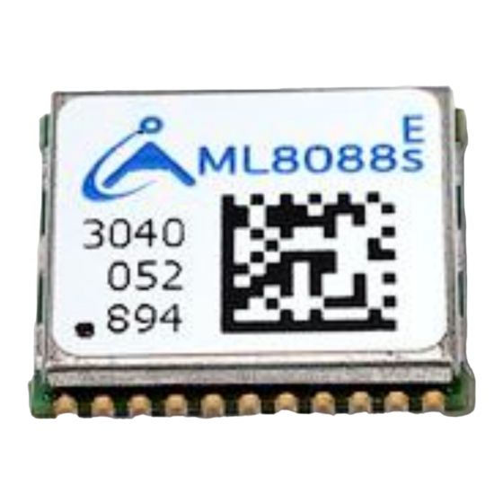
L1 (PT-code), GPS frequency L1 (C/A code) and GALILEO at the frequency E1. The navigation receiver ML8088s is designed on the basis of the latest specialized chipset STA8088FG, a part of the family so-called "systems-on-a-chip" STA8088. The receivers have a high sensitivity, low energy consumption, and a short start time. - Page 4 The Receiver operation is performed with the help of special ST GNSS NMEA commands. This document describes a new sample evaluation board for the receiver ML8088s. The description of the old model evaluation board is available in the document "Evaluation board ML8088s RE v1_0.pdf".
-
Page 5: Technical Specifications
Evaluation Board of ML8088s Receiver Operating Manual 2.0 Technical Specifications Technical specifications of the evaluation board of the ML8088s receiver are shown in table Table 1. Specification Value Navigation receiver ML8088s or ML8088sE Type of antenna Active, passive Antenna connector... -
Page 6: Location Of Indicators And Switching On The Board
Evaluation Board of ML8088s Receiver Operating Manual 2.0 Location of Indicators and Switching on the Board Connector Module power connector for antenna ML8088s GNSS status Module NMEA indicator indicator module signals switch Fig. 3 Location of indicators and switching on the evaluation board Figure 3 illustrates the location of indication and switching elements on the evaluation board of ML8088s receiver. -
Page 7: Signal Switch Of Ml8088S Module
Operating Manual 2.0 Signal Switch of ML8088s Module The switch panel (switch) of the module ML8088s signals is designed to provide users with the opportunity to connect/disconnect any of the major signals of the module ML8088s to electronic nodes of a evaluation board. The signal "disabled" from a evaluation board may be left free (unplugged), or connected to the user's device to accelerate the development of the end product. - Page 8 Evaluation Board of ML8088s Receiver Operating Manual 2.0 Table 3. Signal Jumper position for mode Work Program Program Reset Signal is via UART0 disabled UART0 7-8* remove GNSS status 10-11 11-12 13-14 13-14 14-15 16-17 16-17 17-18 always connected V_BAT VCC_3.3V...
-
Page 9: Components Arrangement On The Evaluation Board
In this case the user can assemble the board partially to the extent necessary for the particular use of ML8088s module. For example, the user can install only the receiver ML8088s module, the capacitors in the module power supply... - Page 10 Evaluation Board of ML8088s Receiver Operating Manual 2.0 470 Ω smd 0603 10k Ω smd 0603 270 Ω smd 0603 100k Ω smd 0603 270 Ω smd 0603 270 Ω smd 0603 1.5k Ω smd 0603 0 Ω smd 0603...
-
Page 11: The Evaluation Board Circuit Diagram
Evaluation Board of ML8088s Receiver Operating Manual 2.0 The Evaluation Board Circuit Diagram The ML8088s receiver evaluation board circuit diagram is presented in Figure 6. Fig. 6. The evaluation board circuit diagram... -
Page 12: Navia Glonass + Gps Application
The receiver embedded software is in standard factory release unless otherwise specified. The application Navia GLONASS + GPS has an embedded system of pop-up prompts and an extensive Support section. The prompts are displayed when the cursor is pointed at an area which can be manipulated by the user. -
Page 13: The Board Activation
(see Fig. 4). Application Configuration The Navia viewer application should be run after the board has been connected to the computer. This is necessary because after the application has been started, it checks all the available serial ports of the user computer. - Page 14 Evaluation Board of ML8088s Receiver Operating Manual 2.0 Fig. 8. The application window appearance at first run. Figure 9A. The message “Data exchange port is not specified". Figure 9B. Data exchange port quick search window. Figure 9C. The message “Data exchange port has been identified”.
- Page 15 Evaluation Board of ML8088s Receiver Operating Manual 2.0 the data exchange port configuration. The application has an automatic identification mode for the NMEA channel serial port number. To activate it click the Run button (see Fig. 10, the application with the specified data exchange port). In case the screen will display the message of input data wrong format (see Fig.
-
Page 16: The Application Operation
Evaluation Board of ML8088s Receiver Operating Manual 2.0 Figure 11B. The data exchange port selection window. Figure 11C. The message “Data exchange port settings have been successfully updated”. The Application Operation After the Run button has been clicked, the application reads and analyses the input data, and displays a number of parameters: ... -
Page 17: Restart
Data Output redirection Fig.13. NAVIA GLONASS + GPS application module data output window tab. This tab provides module set-up by port and output speed selection for positioning system data. For parameter activation additional module restart is required. -
Page 18: 1Pps
Operating Manual 2.0 1PPS Fig.14. NAVIA GLONASS + GPS application module 1PPS signal window tab. This tab provides module operation mode, «1PPS» signal latency and duration time setup. For parameter activation additional setup write command ( «Save» button) and module restart is required. -
Page 19: Messages Set
Evaluation Board of ML8088s Receiver Operating Manual 2.0 Messages SET Fig.16. NAVIA GLONASS + GPS application exchange message set window tab. This tab defines message set, sent by device. Setting activation may require applicatiion restart. The right area of the window indicates messages, sent by application. -
Page 20: Dop Level Setting (Estimated Precision)
Evaluation Board of ML8088s Receiver Operating Manual 2.0 DOP level setting (estimated precision) Fig.18. NAVIA GLONASS + GPS application 1PPS signal level window tab. This tab defines DOP (estimated Dilution of Precision caused by satellite position interference) start and current operation levels threshold. -
Page 21: Differential Mode
Operating Manual 2.0 Differential mode Fig.20. NAVIA GLONASS + GPS application 1PPS signal level window tab. This tab allows selecting the differential correction source. Should be noted, that the SBAS correction parameter may increase the determination of position precision only in the Western region of Russia, in the other regions its use will be at least useless. -
Page 22: Miscellaneous
Evaluation Board of ML8088s Receiver Operating Manual 2.0 Miscellaneous Fig.22. GLONASS + GPS application reciever firmware version window tab. This tab shows module’s navigation library version and the text string for firmware version (parameter 500). -
Page 23: Reciever Pinout
Evaluation Board of ML8088s Receiver Operating Manual 2.0 Reciever Pinout Table 4. Pin № Signal description Type Marked as Common for high frequency Power 20, 22 RF GND Common for digital Power 6, 17 Antenna connection jack Analog IN_RF DC +3,3V... -
Page 24: Practical Use Of The Evaluation Board
The receiver multiplexer of ML8088s chip allows to switch off independently separate or all the signal lines from the board. This allows to test the ML8088s chip in the user’s devices without soldering the chip to the PCB, resulting in the receiver integration jobs onto devices on very early stage. -
Page 25: Typical Connection Circuit
Evaluation Board of ML8088s Receiver Operating Manual 2.0 Typical connection circuit Fig.23. Typical connection circuit for ML8088s chip. = 3,0…3,6V is provided to the 13 contact pad, as shown on the curcuit Power supply V as +3.3V main. All the voltage values are measured relative to bus GND (common). - Page 26 Evaluation Board of ML8088s Receiver Operating Manual 2.0 «Logical 0», in this situation the «pull up» to the main power supply voltage should not be present. Maximum allowed voltage on the module input pins during the main power V switched off should not exceed 0.2 V on all the pins, except of the pin 12 (V_RTC) and 18 (IN /RST).
Need help?
Do you have a question about the ML8088s and is the answer not in the manual?
Questions and answers