
Subscribe to Our Youtube Channel
Summary of Contents for Stanford Research Systems SIM985
- Page 1 Operation and Service Manual Analog Multiplier SIM985 Stanford Research Systems Revision 0.75 March 31, 2023 •...
- Page 2 (1) year from the date of shipment. Service For warranty service or repair, this product must be returned to a Stanford Research Systems autho‑ rized service facility. Contact Stanford Research Systems or an authorized representative before re‑...
-
Page 3: Table Of Contents
Power ......25 3.3 Schematics ......26 SIM985 Analog Multiplier... - Page 4 Contents SIM985 Analog Multiplier...
-
Page 5: General Information
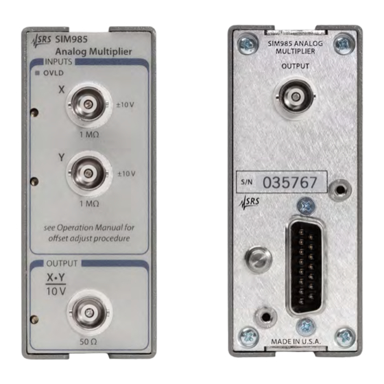
General Information The SIM985 Analog Multiplier, part of Stanford Research Systems’ Small Instrumentation Modules family, is a low noise four‑quadrant analog multiplier for use in signal conditioning applications from DC to 5 MHz. Safety and Preparation for Use .... -
Page 6: Safety And Preparation For Use
Do not exceed ± 15 V relative to Earth at the center terminal of any BNC CAUTION connector. The SIM985 is a single‑wide module designed to be used inside the SIM900 Mainframe. Do not turn on the power until the module is com‑ pletely inserted into the mainframe and locked in place. -
Page 7: Specifications
2, front and rear panels (BNC) Power DB‑15 (male) SIM interface 0 ° C to 40 ° C, non‑condensing Operating temp. Power ± 15 V (150 mA, 350 mA short‑circuit) Weight 1.5 lb 1.5 × 3.6 × 7.0, inches Dimensions SIM985 Analog Multiplier... - Page 8 General Information SIM985 Analog Multiplier...
-
Page 9: Operation
1 Operation Description of the operation of the SIM985. 1.1 Introduction ......1.1.1 Inputs ...... -
Page 10: Introduction
= −5.6 V 10 V 10 V The nominal range for all signals �� , �� , and �� is ±10 V. As the prod‑ uct is scaled by 10 V, the SIM985 does not amplify either input signal. SIM985 Analog Multiplier... -
Page 11: Inputs
Section 2.2. 1.1.3 Bandwidth The bandwidth of the SIM985 is 5 MHz, but can be reduced using jumper J6, as described in Section 2.3. Additionally, the input and output signal circuitry are both limited to maximum slew rate of 120 V/ �� s. -
Page 12: Distortion
Generally, the Y input will have somewhat lower distortion for large AC signals than the X input (see Figure 1.3). Figure 1.3: Typical harmonic distortion of the SIM985. The shaded region in‑ dicates the performance specification. SIM985 Analog Multiplier... -
Page 13: Dc Accuracy
�� = �� − (�� × �� )/10 V. Figure 1.4 shows a Meas contour plot of the typical errors for a SIM985. Figure 1.4: Typical DC errors for the SIM985. SIM985 Analog Multiplier... -
Page 14: Sim Interface
1 Operation 1.4 SIM Interface The primary connection to the SIM985 is the rear‑panel DB–15 SIM inter‑ face connector. Typically, the SIM985 is mated to a SIM900 Mainframe via this connection, either through one of the internal Mainframe slots, or the remote cable interface. -
Page 15: Direct Interfacing
1.4 SIM Interface 1.4.2 Direct interfacing The SIM985 is intended for operation in the SIM900 Mainframe, but users may wish to directly interface the module to their own systems without the use of additional hardware. The mating connector needed is a standard DB–15 receptacle, such as Amp part # 747909‑2 (or equivalent). - Page 16 1 Operation SIM985 Analog Multiplier...
-
Page 17: Trimming
2 Trimming Description of the trimming procedures for the SIM985. 2.1 Overview ......2.2 Offset trims ...... -
Page 18: Overview
With its fundamentally non‑linear transfer function, offset voltages in the SIM985 may contribute to gain errors or DC offset errors. Because of this ambiguity, the following procedures are recommended to first measure the offset voltages prior to adjusting them. -
Page 19: Testing The Offset Voltages
The quick test can be performed using the DC voltage source and the multimeter. A total of 5 measurements are required. Begin by powering up the SIM985 and ensuring it has warmed up for at least 1 hour. • Connect the SIM985 OUTPUT to the multimeter, and leave both inputs open. -
Page 20: Oscilloscope Method
Con‑ nect the other end of the tee to the Y INPUT of the SIM985. • Set the ’scope trigger to Channel 2, and verify the scope is trigger‑... -
Page 21: Lock-In Method
• Set the lock‑in reference source to External, and verify that it locks to 20 Hz. • Connect the BNC 50 Ω terminator to the X INPUT of the SIM985. • Connect the OUTPUT of the SIM985 to the signal input of the lock‑... -
Page 22: Trimming The Output Offset
• Set the DC source to + 10 V output, and connect the output to the Y INPUT on the SIM985. • Connect the BNC 50 Ω terminator to the X INPUT of the SIM985. • Connect the OUTPUT of the SIM985 to the input of the multimeter,... - Page 23 2.3 Bandwidth adjustment A user‑servicable jumper is in the SIM985, allowing users to select out‑ put bandwidth from 500 Hz to 5 MHz, in decade steps. To change this jumper setting: • Remove the SIM985 from the SIM900 mainframe, or if using a stand‑alone power supply, remove power from the unit.
-
Page 24: Gain Trim
2 Trimming 2.4 Gain trim Typically, users should not attempt to adjust the SIM985 gain trim, as this is set at the factory and exhibits excellent long‑term stability. How‑ ever, in some limited circumstances (such as user replacement of U9), adjusting the gain may be helpful. -
Page 25: Procedure
See Figure 2.3. Be sure you have access to adjust this trimmer as described above. • Connect the BNC Tee to the X INPUT of the SIM985, and connect one side of the Tee to the Y INPUT. • Set the DC Source output to 0.000 V •... - Page 26 2 Trimming SIM985 Analog Multiplier...
-
Page 27: Circuit Description
3 Circuit Description Description of the circuitry used in the SIM985. 3.1 Block Diagram ......3.2 Detailed description ..... -
Page 28: Block Diagram
3 Circuit Description 3.1 Block Diagram The SIM985 Analog Multiplier is built around the AD734 high speed four‑quadrant multiplier chip, as shown in the simplified block diagram (Figure 3.1). Each of the inputs (X and Y) are separately buffered with JFET‑input op‑amps, while the output stage is buffered with a composite... -
Page 29: Multiplier
SSCR register. 3.2.5 Power Power for the SIM985 is provided on pins 7 and 14 of the 15‑pin SIM con‑ nector, J5. For normal operation, this power is provided by the SIM900 Mainframe. See Section 1.4.2 for information on directly powering to the SIM985. -
Page 30: Schematics
3 Circuit Description 3.3 Schematics Schematics follow this page. SIM985 Analog Multiplier...
Need help?
Do you have a question about the SIM985 and is the answer not in the manual?
Questions and answers