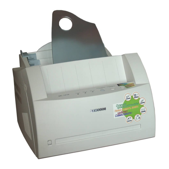
Samsung ML-1200 Series Repair Manual
Laser printer
Hide thumbs
Also See for ML-1200 Series:
- User manual (129 pages) ,
- Service manual (4 pages) ,
- Quick manual (2 pages)

Related Manuals for Samsung ML-1200 Series


Summary of Contents for Samsung ML-1200 Series
- Page 1 Repair Manual Repair Manual LASER PRINTER ML-1200 Series CONTENTS 1. Block Diagram 2. Connection Diagram 3. Schematic Diagrams...
- Page 2 BLOCK DIAGRAM 1. Block Diagram 1.1 GDI Block Diagram(ML-1210/ML-1220M) Repair Manual Samsung Electronics - This Document can not be used without Samsung's authorization -...
- Page 3 BLOCK DIAGRAM 1.2 PCL Block Diagram(ML-1250) Repair Manual Samsung Electronics - This Document can not be used without Samsung's authorization -...
- Page 4 THVRE AD EGMOT _ PHA DEV_FUSE * M H VP WM BI ASPW M +5V GND ENG I NE + SM PS Unification ' d Repair Manual Samsung Electronics - This Document can not be used without Samsung's authorization -...
- Page 5 NEW_DVE* HV PS THVRE AD MOTOR_PA DEV_FUSE M H VP WM BI ASPW M +5V GND ENG I NE + SM PS Unification ' d Repair Manual Samsung Electronics - This Document can not be used without Samsung's authorization -...
- Page 6 SCHEMATIC DIAGRAMS 3. Schematic Diagrams 3.1 GDI Main Circuit Diagram (1/5) Repair Manual Samsung Electronics - This Document can not be used without Samsung's authorization -...
- Page 7 SCHEMATIC DIAGRAMS Main Circuit Diagram (2/5) Repair Manual Samsung Electronics - This Document can not be used without Samsung's authorization -...
- Page 8 SCHEMATIC DIAGRAMS Main Circuit Diagram (3/5) Repair Manual Samsung Electronics - This Document can not be used without Samsung's authorization -...
- Page 9 SCHEMATIC DIAGRAMS Main Circuit Diagram (4/5) Repair Manual Samsung Electronics - This Document can not be used without Samsung's authorization -...
- Page 10 SCHEMATIC DIAGRAMS Main Circuit Diagram (5/5) Repair Manual Samsung Electronics - This Document can not be used without Samsung's authorization -...
- Page 11 SCHEMATIC DIAGRAMS 3.2 PC L Main Circuit Diagram (1/9) Repair Manual Samsung Electronics - This Document can not be used without Samsung's authorization -...
- Page 12 SCHEMATIC DIAGRAMS PCL Main Circuit Diagram (2/9) Repair Manual Samsung Electronics - This Document can not be used without Samsung's authorization -...
- Page 13 SCHEMATIC DIAGRAMS PCL M a i n Circuit Diagram (3/9) Repair Manual Samsung Electronics - This Document can not be used without Samsung's authorization -...
- Page 14 SCHEMATIC DIAGRAMS PCL Main Circuit Diagram (4/9) Repair Manual Samsung Electronics - This Document can not be used without Samsung's authorization -...
- Page 15 SCHEMATIC DIAGRAMS PCL M ainCircuit Diagram (5/9) Repair Manual 3-10 Samsung Electronics - This Document can not be used without Samsung's authorization -...
- Page 16 SCHEMATIC DIAGRAMS PCL Main Circuit Diagram (6/9) Repair Manual 3-11 Samsung Electronics - This Document can not be used without Samsung's authorization -...
- Page 17 SCHEMATIC DIAGRAMS PCL M a i n Circuit Diagram (7/9) Repair Manual 3-12 Samsung Electronics - This Document can not be used without Samsung's authorization -...
- Page 18 SCHEMATIC DIAGRAMS PCL M a i n Circuit Diagram (8/9) Repair Manual 3-13 Samsung Electronics - This Document can not be used without Samsung's authorization -...
- Page 19 SCHEMATIC DIAGRAMS PCL M a i n Circuit Diagram (9/9) Repair Manual 3-14 Samsung Electronics - This Document can not be used without Samsung's authorization -...
- Page 20 SWALLOW-HVPS THV-EA THV-READ MHV-PWM DESIGNED CHECKED APPROVED DRW. NO REV. BIAS-PWM 35V 47uF REF. NO D-GND JH.CHO SIZE A4 DATE 01/01/04 1 OF 2 Repair Manual 3-15 Samsung Electronics - This Document can not be used without Samsung's authorization -...
- Page 21 500V 103 VR301 SAMSUNG ELECTRONICS TITLE SWALLOW-HVPS C301 DESIGNED CHECKED APPROVED DRW. NO REV. REF. NO JH.CHO SIZE A4 2 OF 2 DATE 01/01/04 Repair Manual 3-16 Samsung Electronics - This Document can not be used without Samsung's authorization -...
- Page 22 FUSER_ON CN5-16 +24VS +24V A2918SWH 35301-0350 35303-0250 EGMOT_PHA PHASE1 EGMOT_PHB PHASE2 CLUTCH 1008-Y +EGMOT_A1 1008-Y +ENABLE1 2.2K +EGMOT_B1 +ENABLE2 5.6K 5.6K 35303-0450 1.2K 17.4K-F Repair Manual 3-17 Samsung Electronics - This Document can not be used without Samsung's authorization -...
- Page 23 FUSER_ON CN5-16 +24V +24VS A2918SWH 35303-0250 35301-0350 EGMOT_PHA PHASE1 EGMOT_PHB PHASE2 CLUTCH 1008-Y +EGMOT_A1 1008-Y +ENABLE1 +EGMOT_B1 2.2K +ENABLE2 5.6K 5.6K 35303-0450 1.2K 17.4K Repair Manual 3-18 Samsung Electronics - This Document can not be used without Samsung's authorization -...
- Page 24 SCHEMATIC DIAGRAMS 3.5 Panel Circuit Diagram Repair Manual 3-19 Samsung Electronics - This Document can not be used without Samsung's authorization -...
- Page 25 - This Service Manual is a property of Samsung Electronics Co.,Ltd. Any unauthorized use of Manual can be punished under applicable International and/or domestic law. -...
- Page 26 This manual is made and described centering around circuit diagram and circuit description needed in the repair center in the form of appendix. Samsung Electronics Digital Printing CS Group Copyright (c) 2001. 10...
Need help?
Do you have a question about the ML-1200 Series and is the answer not in the manual?
Questions and answers