Table of Contents
Advertisement
Quick Links
Jun. 2014
Table of Contents
Cautionary Notes ..............................................................2
Specifications .....................................................................2
Location of Controls (Front) ............................................4
Location of Controls (Front) Parts List...........................4
Location of Controls (Rear)..............................................5
Location of Controls (Rear) Parts List ............................5
Exploded View ..................................................................6
Exploded View Parts List.................................................7
Disassembly Procedure ....................................................7
Plane View (View 1, 2)......................................................8
Plane View (View 3)..........................................................9
Plane View (View 4)........................................................10
Exploded View (Fig. A)..................................................11
Exploded View (Fig. B)...................................................12
Wiring Diagram/Block Diagram..................................14
Copyright © 2014 Roland Corporation
All rights reserved. No part of this publication may be reproduced in any form without the written permission
of Roland Corporation.
Parts List ...........................................................................16
Verifying the Version......................................................18
Virus Check ......................................................................18
Data Backup and Restore Operations ..........................18
Performing a Factory Reset............................................18
Updating the System ......................................................19
Test Mode .........................................................................19
Circuit Board (Main Board) ...........................................24
Circuit Diagram (Main Board: 1/4)..............................26
Circuit Diagram (Main Board: 2/4)..............................28
Circuit Diagram (Main Board: 3/4)..............................30
Circuit Diagram (Main Board: 4/4)..............................32
Circuit Board (Panel, GK, Exp, Enc Board) .................34
Circuit Diagram (Panel, GK, Exp, Enc Board) ............36
Revise Information
Dec. 16, 2014
17058926E0
SERVICE NOTES
Issued by RJA
p. 21
Corrected errors.
GP-10
CC-KWS
Advertisement
Table of Contents

Related Manuals for Roland GP-10


Summary of Contents for Roland GP-10
-
Page 1: Table Of Contents
Wiring Diagram/Block Diagram........14 Revise Information Dec. 16, 2014 p. 21 Corrected errors. Copyright © 2014 Roland Corporation All rights reserved. No part of this publication may be reproduced in any form without the written permission of Roland Corporation. 17058926E0 CC-KWS... -
Page 2: Cautionary Notes
• Because the part is made to order (at current market price). Patch Memory • Because it is carried in electronic data on the Roland web site. • Because it is a package or an accessory irrelevant to the function maintenance of the main body. - Page 3 Divided pickup: Roland GK-3 GUITAR OUT: -10 dBu GK cable: Roland GKC-5 (5 m), GKC-10 (10 m) PHONES: -10 dBu GK parallel cable (GK pickup <–> GK connector x 2): Roland GKP-2 Unit selector: Roland US-20 Footswitch: FS-5U Output Impedance Dual footswitch: FS-6 OUTPUT L/MONO, R: 2 kΩ...
-
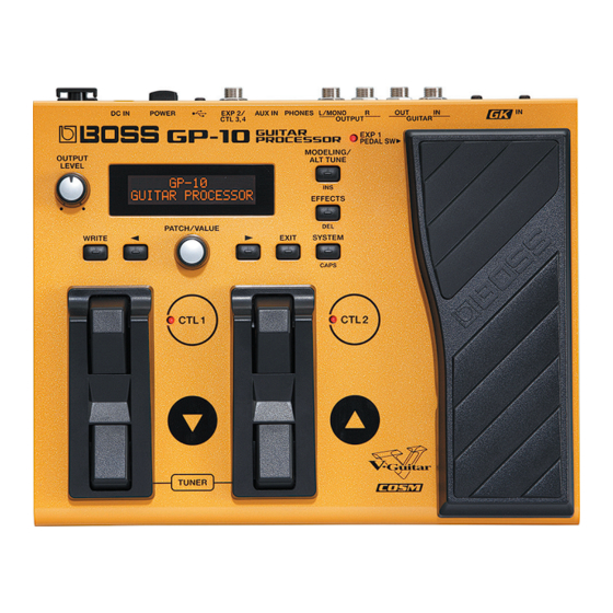
Page 4: Location Of Controls (Front)
Jun. 2014 GP-10 Location of Controls (Front) fig.panel-front.eps Location of Controls (Front) Parts List Part Code Part Name Description Q’ty 5100007869 R-KNOB INDEX G2477526R1 5100006350 POTENTIOMETER(F3229188R1) RD901F-40-15F-B50K-00DQ7 40128923 HEX NUT M7 H5039521R0 5100037970 DISPLAY COVER 5100010065 PE1602MRT-012-I-Q(F5029425R0) 5100037971 DISPLAY CUSHION... -
Page 5: Location Of Controls (Rear)
Jun. 2014 GP-10 Location of Controls (Rear) fig.panel-rear.eps Location of Controls (Rear) Parts List Part Code Part Name Description Q’ty 00564556 DIN CONNECTOR TCS5093-10-4152 03344923 FOOT H=5 (G2357120R0) 5100001342 6.5MM JACK HTJ-064-12IMP (13449155R1) 5100003918 JACK NUT M9X12X2 NI RTC(H5039510R0) 5100003926 PLAIN WASHER 9X13.5X0.5T... -
Page 6: Exploded View
Jun. 2014 GP-10 Exploded View fig.bunkaizu-total.eps Refer to Fig. A Refer to Fig. B... -
Page 7: Exploded View Parts List
Jun. 2014 GP-10 Exploded View Parts List Part Code Part Name Description Q’ty 5100007869 R-KNOB INDEX G2477526R1 5100008051 R-KNOB (G2477525R1) 5100037968 TOP COVER 5100037970 DISPLAY COVER 22360712 CORD HOOK 236-712 5100018071 POWER SW ESCUTCHEON G2207430R1 12499175 BUTTON JSPUE0011A 5100037971 DISPLAY CUSHION... -
Page 8: Plane View (View 1, 2)
Jun. 2014 GP-10 Plane View (View 1, 2) fig.bunkaizu-view-12.eps View 1 View 2 View 1 Part Code Part Name Description Q’ty 40237101 SCREW M3X8 PAN MACHINE W/SW+SMALL PW BZC 40342712 SCREW M3X6 PAN MACHINE W/SW+SMALL PW BZC 40019123 SCREW 3X8... -
Page 9: Plane View (View 3)
Jun. 2014 GP-10 Plane View (View 3) fig.bunkaizu-view-3.eps View 3 View 3 Part Code Part Name Description Q’ty 40011312 SCREW 3X8 BINDING TAPTITE P FE BZC 40012867 SCREW M3X8 PAN MACHINE W/SW+PW ZC... -
Page 10: Plane View (View 4)
Jun. 2014 GP-10 Plane View (View 4) fig.bunkaizu-view-4.eps View 4 View 4 Part Code Part Name Description Q’ty 40342712 SCREW M3X6 PAN MACHINE W/SW+SMALL PW BZC... -
Page 11: Exploded View (Fig. A)
Jun. 2014 GP-10 Exploded View (Fig. A) fig.bunkaizu-A.eps Part Code Part Name Description Q’ty 5100037545 SW PEDAL FRONT 5100037546 SW PEDAL REAR 04560712 SUPPORT SPRING (G2177103R0) 5100003910 PEDAL FOOT H=7.6 (G2357126R0) 5100037544 SW PEDAL ESCUTCHEON... -
Page 12: Exploded View (Fig. B)
Jun. 2014 GP-10 Exploded View (Fig. B) fig.bunkaizu-B.eps Part Code Part Name Description Q’ty 5100011395 PEDAL PLATE 5100011392 VR PEDAL 03561356 SHAFT STAY STAY 5100037249 PANEL SHEET ASSY * This unit includes the following parts. ******** EXP BOARD ******** PANEL BOARD Refer to Exploded View (p. - Page 13 Jun. 2014 GP-10...
-
Page 14: Wiring Diagram/Block Diagram
Jun. 2014 GP-10 Wiring Diagram/Block Diagram fig.block.eps@L GUITAR INPUT JK10 AUX IN/ STEREO MINI 1st string 2nd string 3rd string 4th string 5th string INPUT BOARD 6th string DC JACK... - Page 15 Jun. 2014 GP-10 Part Code Part Name Description Q'ty 5100037384 WIRING W1 (EXP) fig.block.eps@R 5100037393 WIRING W2 (PANEL) 5100037394 WIRING W3 (INPUT) 5100037395 WIRING 3P L=55X5X5 P=2.0 JK GUITAR OUT JK OUTPUT L(MONO) JK OUTPUT JK PHONES JK USB JK EXP2/CTL...
-
Page 16: Parts List
Use • Supply is prohibited due to copyright restrictions. • Reissuance is restricted. • It is carried in electronic data on the Roland web site. • It is supplied as an assembled part only listed parts for replacement. - Page 17 Jun. 2014 GP-10 SCREWS 40342712 SCREW M3X6 PAN MACHINE W/SW+SMALL PW BZC 40237101 SCREW M3X8 PAN MACHINE W/SW+SMALL PW BZC 40012867 SCREW M3X8 PAN MACHINE W/SW+PW ZC 40011278 SCREW 3X8 BINDING TAPTITE P FE ZC 40011312 SCREW 3X8 BINDING TAPTITE P FE BZC...
-
Page 18: Verifying The Version
The data is recorded on the MIDI sequencer program. appears. * Progress is not displayed on the GP-10. To monitor the progress, check the After a short wait, the version information is displayed. display in the MIDI sequencer program you're using. -
Page 19: Updating The System
Connect the AC adaptor to the GP-10. http://www.roland.com Hold down and switch on the power. GP-10 Updater is displayed on the GP-10 screen. • Cable for measurement of DC IN current consumption Connect the computer to the connector. fig.check-cable.eps Connected. - Page 20 Jun. 2014 GP-10 Test Items 04:USB CHECK fig.test4-1.eps 01:VERSION (p. 20) 02:DEVICE CHK (p. 20) 03:CURRENT CHK (p. 20) 04:USB CHECK (p. 20) Use the USB cable to connect the connector and the computer. 05:ENC/LCD CHK (p. 20) Verify that UNPLUG USB is displayed, disconnect the USB cable.
- Page 21 Jun. 2014 GP-10 08:GK SW/VOL Insert the short plug (standard monaural) to the GUITAR IN jack and verify that no signal is output from the GUITAR OUT jack. fig.test8.eps fig.test9-3.eps * Before connecting the GK-3, turn the GK volume on the GK-3 all the way clockwise and adjust the selector switch to MIX.
- Page 22 Jun. 2014 GP-10 Verification of AF-AD waveform Verification of MUTE operation 11. Input a signal like the one shown below to the normal input connector on 18. Press to move the flashing cursor on the screen to mut. the GK-3.
- Page 23 31. Verify that signals like the ones shown below are output. Verify that no abnormal noise is heard from the monitor speakers. OUTPUT L/MONO: 6.0 Vp-p±0.5 V Drop the GP-10 from a height of about 10 centimeters, and verify that no OUTPUT R: 6.0 Vp-p±0.5 V abnormal noise is heard from the monitor speakers.
-
Page 24: Circuit Board (Main Board)
Jun. 2014 GP-10 Circuit Board (Main Board) fig.b-main1.eps... - Page 25 Jun. 2014 GP-10 fig.b-main2.eps...
-
Page 26: Circuit Diagram (Main Board: 1/4)
Jun. 2014 GP-10 Circuit Diagram (Main Board: 1/4) fig.d-main1.eps@L PVCC TP99 VCC-PWR MCH6341-TL-E R250 R253 D3 SR24 330k 0.47uF TP96 1608 DC IN KM02018ABM1P R251 470uF 0.1uF DR-670 DC JACK HOLDER(G2147127) TP117 DTC114EUAT106(PB FREE) FB+1.15V C171 10uF 0.1uF TP10 POWER SW... - Page 27 Jun. 2014 GP-10 fig.d-main1.eps@R A+5.0 A+3.3 A+3.3 TP51 TP54 A+5.0 IC26 IC16 BA17805FP-E2 NJM2882F33-TE1 TP48 TP190 C230 APVCC VOUT C141 0.1uF C135 0.1uF 0.1uF CTRL N-BP C234 C166 C236 C158 10uF 0.1uF 10uF C223 220uF C194 C224 C140 2125 0.1uF 0.1uF...
-
Page 28: Circuit Diagram (Main Board: 2/4)
Jun. 2014 GP-10 Circuit Diagram (Main Board: 2/4) fig.d-main2.eps@L TO GK BOARD A2001WR2-14P GK+7V GK+7V 1SS362FV(TPL3) 1SS362FV(TPL3) GK+7V R244 1608 C322 GKVOL 22uF R243 C321 C320 C326 C327 C323 0.01uF 0.01uF 22uF 1608 GK-GTR-SIGNAL GK-7V STR(1:6) SW1-B SW1-A GAIN 1 : -16.8dB... - Page 29 Jun. 2014 GP-10 fig.d-main2.eps@R TP185 D+3.3 GK+7V GK+7V GK+7V 1SS362FV(TPL3) 1SS362FV(TPL3) TP186 R124 R190 220k 3.9k 0.5% 1SS387(TPH3.F) 0.5% GK-VOL R194 GK+7V 4.7k NJM2904M-TE3 R188 0.5% 2.2M TP134 0.1uF D+3.3 NJM2904M-TE3 TP187 1SS387(TPH3.F) GK-SW0 A+5.0 R189 R193 1.8k 3.3k C345...
-
Page 30: Circuit Diagram (Main Board: 3/4)
Jun. 2014 GP-10 Circuit Diagram (Main Board: 3/4) fig.d-main3.eps@L R179 R161 AUX IN R181 R174 C149 C150 1000pF 1000pF HTJ-035-10ABZ AK4556 A+3.3 AD/DA 2.31Vpp max DA 2.31Vpp max +0.46dBu max +0.46dBu max NOR STR TP27 TP36 Gain -8.1dB 1608 TP125... - Page 31 Jun. 2014 GP-10 fig.d-main3.eps@R Gain +9.9dB TP142 TP133 GK+7V UnPop C136 10pF PHONES-SW D10 UnPop TP153 R168 47k TP63 TP60 0.5% C148 R172 10uF R175 3/4W 3/4W 0.5% C112 HEADPHONES R176 C145 220uF R164 IC22 10uF 100k NJM4580M(TE3) DTC614TU T106...
-
Page 32: Circuit Diagram (Main Board: 4/4)
Jun. 2014 GP-10 Circuit Diagram (Main Board: 4/4) fig.d-main4.eps@L D+3.3 D+3.3 RA33 EXB28V220JX CTL2-LED R122 EXP-PEDAL-LED R127 CTL1-LED R155 GAIN-CLK R116 XSF-WP For J-TAG R152 RA32 XMUTE R159 EXB28V220JX GAIN-DATA MA(0:15) R149 XOFF-PWR MA(15) RA28 XICE-REST AA15 MA(14) XMRDMRAS XMRD-MRAS... - Page 33 Jun. 2014 GP-10 fig.d-main4.eps@R EA(0:14) D+1.15 RA10 ED(0:15) EA(14) D+3.3 EA(13) C122 EA(12) R120 0.1uF EA(11) EA(10) EA(9) TC7WU04FU(TE12L.F) R118 TC7WU04FU(TE12L.F) RA12 EA(8) EA(7) EA(6) 0.1uF D+1.15 EA(5) R114 RA21 EA(4) EA(14) TC7WU04FU(TE12L.F) EA(3) EA(13) C102 C125 EA(2) EA(12) 0.1uF EA(1) E3SB16.9344F12D33...
-
Page 34: Circuit Board (Panel, Gk, Exp, Enc Board)
Jun. 2014 GP-10 Circuit Board (Panel, GK, Exp, Enc Board) fig.b-main1.eps... - Page 35 Jun. 2014 GP-10 fig.b-main2.eps...
-
Page 36: Circuit Diagram (Panel, Gk, Exp, Enc Board)
L-7104SRT RD901F-40-15F-B50K-00DQ7 [CTL 1 LED] [PEDAL DOWN] A2001WR2-2P 50kB SKQKAKD010 for Back Light(orange) TP19 50kB RD901F-40-125F-B50K-00D D+3.3 To Main Board CN 3 ENC BOARD GP-10 WIRING2(PANEL) RE111F-40B3-15F-20P RE111F-40B3-15F-20P GP-10 RIBBON CABLE 3P L=55X5X5 P=2.0 GP-10 RIBBON CABLE 3P L=55X5X5 P=2.0... - Page 37 TCS5093-1042577 STR(1) STR(2) STR(3) STR(4) STR(5) STR(6) STR(7) GKS(1:4) STR(7) STR(6) STR(5) STR(4) STR(3) STR(2) STR(1) GP-10 WIRING W3 (INPUT) To Main Board CN 6 GK BOARD EXP BOARD GP-10 WIRING W1 (EXP) To Main Board CN 2 RK11K1140AFG...
Need help?
Do you have a question about the GP-10 and is the answer not in the manual?
Questions and answers