Advertisement
Quick Links
Advertisement

Related Manuals for Laird Lyra S


Summary of Contents for Laird Lyra S
- Page 1 Version 1.3...
- Page 2 Software Development Selection Switch SW1 Added section 8.4.1 BOOT pin (PA06) 31 Aug 2022 Raj Khatri Jonathan Kaye and BUTTON 0 (silkscreen BTN0) Dave Drogowski https://www.lairdconnect.com/ Americas: +1-800-492-2320 © Copyright 2022 Laird Connectivity Europe: +44-1628-858-940 All Rights Reserved Hong Kong: +852-2762-4823...
- Page 3 Overview..................................4 Laird Connectivity Lyra S Part Numbers ........................4 Kit Contents ................................. 5 Main Board – Features ..............................5 Key Features ............................... 5 Understanding the Development Board ......................... 6 Software Development Selection Switch SW1 ....................... 7 Specifications ................................7 Recommended Operating Conditions ........................
- Page 4 Wireless Bluetooth® Module. The Lyra S Development Kit is focused on rapid prototyping and concept creation of IoT applications. It is designed around the Lyra S Module, based on the EFR32BG22 System-on-Chip, which is an ideal device family for developing energy-friendly connected IoT applications.
- Page 5 Lyra S such as I2C, SPI, UART and GPIOs. The mikroBUS socket allows inserting mikroBUS add-on boards which interface with the Lyra S through SPI, UART or I2C. The Qwiic connector can be used to connect hardware from the Qwiic Connect System through I2C.
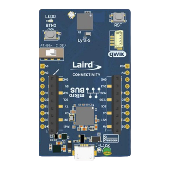
- Page 6 C-DEV. See Software Development Selection Switch SW1. Figure 1: Lyra S development board layout Note: To route RF from Lyra S module to RF connector on development board, see Routing RF to External Antenna on J3 RF connector. https://www.lairdconnect.com/ Americas: +1-800-492-2320 ©...
- Page 7 Operating Temperature The typical supply voltage to the Lyra S is 3.0 V, but the maximum voltage is a function of temperature and average lifetime current load. Over a 10-year lifespan, the average lifetime current load should not exceed 60 mA when the supply voltage is 3.3 V.
- Page 8 Unit On-board Debugger On-board debugger current consumption when USB cable is not inserted (EFM32GG12 EM4S mode current consumption) Sleep Current Consumption From Lyra S data sheet From EFM32GG12 data sheet https://www.lairdconnect.com/ Americas: +1-800-492-2320 © Copyright 2022 Laird Connectivity Europe: +44-1628-858-940...
- Page 9 The core of the Lyra S Development Kit is the Lyra S Bluetooth® Module. Refer to Understanding the Development Board placement and layout of the hardware components. An overview of the Lyra S Development Kit is illustrated in the figure below.
- Page 10 The kit has one user push button marked BTN0 and one LED marked LED0 that are each connected to a GPIO on the Lyra S. The button is connected to pin PA06 and it is debounced by an RC filter with a time constant of 1 ms. The logic state of the button is high while the button is not being pressed, and low when the button is pressed.
- Page 11 For the Lyra S module the BOOT pin is on PA06 (pin18). On the Lyra dev board BTN0 (Button 0) is by default mapped to the BOOT pin for easier utilisation. The BOOT pin (PA06) is used to determine when execution of the bootloader is required. Upon reset, execution of the bootloader begins.
- Page 12 The Lyra S Development Kit features a USB Micro-B connector, 20 breakout pads, a mikroBUS connector for connecting mikroBUS add-on boards, and a Qwiic connector for connecting Qwiic Connect System hardware. The connectors are placed on the top side of the board, and their placement and pinout are shown in the figure below. For additional information on the connectors, see the following sub chapters.
- Page 13 Twenty breakout pads are provided and allow connection of external peripherals. There are 10 pads on the left side of the board, and 10 pads on the right. The breakout pads contain a number of I/O pins that can be used with most of the Lyra S features.
- Page 14 5V or VMCU power rails, which are available on the mikroBUS socket. The pinout of the Lyra S on the kit is made such that all required peripherals are available on the mikroBUS socket. The I...
- Page 15 The Lyra S Development Kit features a Qwiic® connector compatible with Qwiic Connect System hardware. The Qwiic connector provides an easy way to expand the functionality of the Lyra S Development Kit with sensors, LCDs, and other peripherals over the I C interface.
- Page 16 VCOM interfaces maintain proper isolation and prevent leakage currents. The virtual COM port is a connection to a UART of the target Lyra S and allows serial data to be sent and received from the device. The on-board debugger presents this as a virtual COM port on the host computer that shows up when the USB cable is inserted.
- Page 17 Lyra S module on development board can be used with external antennas (certified by Laird Connectivity) by routing the RF to the RF antenna connector (IPEX MHF4) on the development board by removing 0R resistor R936 and fitting 0R resistor R937, Table 4 schematic below and PCB location for R936, R937.
Need help?
Do you have a question about the Lyra S and is the answer not in the manual?
Questions and answers