Panasonic KX-TG2650N Service Manual
2.4ghz digital cordless phone champagne gold version
Hide thumbs
Also See for KX-TG2650N:
- Operating instructions manual (68 pages) ,
- Operating instructions manual (68 pages)

Related Manuals for Panasonic KX-TG2650N


Summary of Contents for Panasonic KX-TG2650N
- Page 1 ORDER NO. KM40009704C1 Telephone Equipment KX-TG2650N 2.4GHz Digital Cordless Phone Champagne gold Version (for U.S.A.) SPECIFICATIONS...
-
Page 2: Location Of Controls
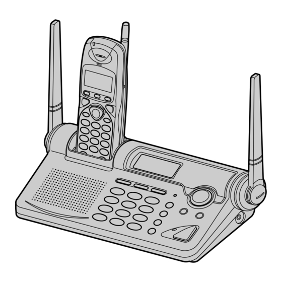
1. LOCATION OF CONTROLS 1.1. Base Unit... - Page 3 1.2. Handset...
- Page 4 2. DISPLAYS Both the handset and the base unit show you instructions and information on the displays. These display prompts are shown below. 2.1. Common Prompts for the Handset and the Base Unit...
- Page 5 3. SETTINGS 3.1. Connections...
- Page 6 Note: - USE ONLY WITH Panasonic AC ADAPTOR PQLV10 (Order No. PQWATG2650N). - The AC adaptor must remain connected at all times. (It is normal for the adaptor to feel warm during use.) - If your unit is connected to a PBX which does not support Caller ID...
-
Page 7: Battery Charge
3.2. Battery Charge 3.2.1. Battery Strength 3.2.2. Recharge 3.2.3. Battery Information... -
Page 8: Selecting The Dialing Mode
3.3. Selecting the Dialing Mode... -
Page 9: Selecting The Line Mode
3.4. Selecting the Line Mode... - Page 10 4. OPERATION 4.1. Making Calls 4.1.1. With the Handset...
- Page 13 4.1.2. With the Base Unit (Digital Duplex Speakerphone)
-
Page 15: Answering Calls
4.2. Answering Calls... -
Page 17: Flash Button
4.3. Flash Button 4.4. Caller ID Service This unit is compatible with a Caller ID service offered by your telephone company. If you subscribe to a Caller ID service, the calling party’s information will be shown on the handset and base unit displays after the first ring. - Page 18 numbers from the Caller List into the directory. If you subscribe to both Caller ID and Call Waiting services, when a second call is received while talking, the new caller’s name and phone number will be displayed. 4.4.1. How caller information is displayed when a call is received 4.4.2.
- Page 19 4.4.3. Viewing the Caller List...
- Page 21 4.4.4. Calling Back from the Caller List 4.4.5. Editing the Caller’s Phone Number 4.4.5.1. With the handset...
- Page 22 4.4.5.2. With the base unit...
- Page 23 4.4.6. Storing Caller List Information in the Directory...
- Page 24 4.4.7. Erasing Caller List Information...
- Page 25 5. DISASSEMBLY INSTRUCTIONS...
- Page 27 Shown in Fig.- To Remove Remove Lower Cabinet Screws (2.6 × 14) × 4 Main P.C. Board Remove the P.C. Board Operational P.C. Board Screws (2.6 × 8) × 7 Battery Cover Remove the Battery Cover Rear Cabinet Screws (2 × 8) × 2 Main P.C.
-
Page 28: Assembly The Lcd To P.c. Board (Handset)
6.2. Assembly the LCD to P.C. Board (Handset) - Page 29 6.3. Replace the RF unit For HS Follow this procedure below when replacing HS RF(*1) unit. 1. Remove speaker cables of LCD unit on HS main board. / And remove LCD unit. 2. Remove solder on six legs of RF unit. 3.
-
Page 30: Troubleshooting Guide
7. Replace defective RF unit with new HS RF unit. NOTE: Do not use BU RF unit for HS one. HS RF unit is different from BU one. 8. Solder all pads of RF unit. 9. Stick tape on RF pads like figure below. 10. -
Page 31: Check Power
7.1. Check Power... - Page 32 7.2. Error Indication 7.3. Check SP-Phone Voice Transmission...
- Page 33 7.4. Check SP-Phone Voice Reception 7.5. Check Battery Charge...
-
Page 34: Check Link
7.6. Check Link... -
Page 35: Check The Rf Unit
7.7. Check the RF Unit 7.7.1. Finding out the Defective Unit Prepare HS Test Fixture and BU Test Fixture. Place the HS Test Fixture on the cradle of the base unit for checking, then confirm that they are linked. Place the handset for checking on the cradle of the BU Test Fixture, then confirm that they are linked. - Page 36 TALK. This means that the base unit sensitivity is OK. NOTE: 1) Only KX-TG2650N with marks HS Test Fixture can be used for troubleshooting. Regular KX- TG2650N production samples does not have the software needed for troubleshooting. 7.7.2.2. Base Unit Test Fixture for Handset The headset Jack has been wired as a switch to control Normal and Test modes on this “BU Test...
- Page 37 OK. NOTE: 1) Only KX-TG2650N with marks BU Test Fixture can be used for troubleshooting. Regular KX- TG2650N production samples does not have the software needed for troubleshooting. 7.7.3. RF Check Flowchart...
- Page 38 7.7.4. Check Table for RF Block...
- Page 39 No. Item BU (Base unit) (*1) HS (Handset) (*1) Link confirmation 1. Insert headset plug to headset jack 1. Insert headset plug to headset Normal of "HS Test Fixture". / 2. Press [TALK] of "BU Test Fixture". / 2. Press key of "HS Test Fixture"...
- Page 40 TX-Power (Low) Limit (without 20dB Attenuator) Loss (CN4-CN3) 15.5dB 15.6dB 15.7dB 15.8dB 15.9dB Test Equipment Unit Low High Low High Low High Low High Low High Spectrum Analyzer Marconi 2945or dBm -20.5 ~ -5.5 -20.6 ~ -5.6 -20.7 ~ -5.7 -20.8 ~ -5.8 -20.9 ~ -5.9 SP-ANA w/JIG ~ 281.8 8.7 ~ 275.4 8.5...
- Page 41 Loss (CN4-CN3) 16.0dB 16.1dB 16.2dB 16.3dB 16.4dB Test Equipment Unit Low High Low High Low High Low High Low High Spectrum Analyzer Marconi 2945or dBm -21.2 ~ -13.2 -21.3 ~ -13.3 -21.4 ~ -13.4 -21.5 ~ -13.5 -21.6 ~ -13.6 SP-ANA w/JIG ~ 47.9 ~ 46.8...
- Page 42 7.8. Check Handset Voice Transmission...
- Page 43 7.9. Check Handset Voice Reception...
-
Page 44: Check Call Id
7.10. Check Call ID... - Page 45 8. TEST MODE AND ADJUSTMENT 8.1. Test Mode Flow Chart for Base Unit...
-
Page 46: Key Check Mode
(*1) See Base Unit Reference Drawing. (*2) Special check method for Base Unit individually. (*3) See TX-Power Specification Table. 8.2. Key Check Mode (*1) See Base Unit Reference Drawing. 8.3. Test Mode Flow Chart for Handset... -
Page 47: Adjustment Battery Low Detector Voltage
8.4. Adjustment Battery Low Detector Voltage After replacing handset’s DSP (IC201), Re-writing Battery Low voltage to EEPROM is required. Following Test mode flow chart (Refer to Test Mode Flow Chart for Handset), DC power supply and Battery connector are required in this adjustment. 1. -
Page 48: Time Division Duplex (Tdd) Operation
8.5. Base Unit Reference Drawing 8.6. Handset Reference Drawing 8.7. Frequency Table 9. DESCRIPTION 9.1. Frequency The frequency range of 2.4015 GHz ~ 2.4705 GHz is used. Transmitting and receiving channel between base unit and handset is same frequency. Refer to the Frequency Table. 9.2. -
Page 49: Spread Spectrum
9.2.1. TDD Frame Format The TDD frame is 2mS in length, and is composed of two symmetrical 960 S TX and RX subframes. Each subframe contains 96 bits of 10 S duration, with 40 S guard times between both TX and RX subframes. Each subframe consists of the following five fields: - A 12-bit Preamble field - An 8-bit Data Channel field... -
Page 50: Signal Flowchart In The Whole System
9.4. Signal Flowchart in the Whole System Reception CN101 of the base unit is connected to the TEL line, and the signal is input through the bridge diode D101. While talking the relay (Q121) is turned ON and amplified at the amplifiers Q461, then led to DSP (IC501). - Page 51 9.5. Explanation of DSP Data Communication 9.5.1. Calling...
-
Page 52: Terminal Guide Of Ic's, Transistors And Diodes
9.5.2. To Terminate Communication 9.5.3. Ringing 10. TERMINAL GUIDE OF IC'S, TRANSISTORS AND DIODES 10.1. Base Unit... - Page 53 10.2. Handset 11. BLOCK DIAGRAM (Base Unit) 12. CIRCUIT OPERATION (Base Unit) 12.1. SP-PHONE RX Circuit Circuit Operation: / Telephone Line (T/R) Q131 C463 R448 C442 R464 C441 pin 38 of IC501 pins 32 and 33 of IC501 Speaker...
- Page 54 12.2. SP-PHONE TX Circuit Circuit Operation: / MIC C724 C725 C726 R726 pin 47 of IC501 pin 36 of IC501 R431 C432 C433 Telephone Line...
-
Page 55: Auto Disconnect Circuit
12.3. Auto Disconnect Circuit Function: / This circuit is used to detect the fact that another telephone connected to the same line is OFF-HOOK while the unit is in a receiving status or OGM transmitting status. Circuit Operation: / The voltage pin 40 of IC501 is monitored. If a parallel-connected telephone is put into an OFF HOOK status, the presence/absence of a parallel connection is determined when the voltage changes by 0.2V or more. - Page 56 with low power loss and low heat radiation. Circuit Operation: / IC301 is a regulated power supply. The voltage at point A is regulated to 4.5 V by IC301. / The voltage at point B is dropped by D306 to 4.1 V. / The voltage at point C is dropped by D511 to 3.8 V.
- Page 57 12.7. Line Receiving Signal The audio signal from line passes through Q131 and Q461 to pin38 and 39 of IC501(DSP). IC501 modulates this input audio signal to output to the RF unit.
-
Page 58: Calling Line Identification Circuit (Caller Id)
12.8. Calling Line Identification Circuit (Caller ID) Function: / The caller ID is a chargeable ID which the user of a telephone circuit obtains by entering a contract with the telephone company to utilize a caller ID service. For this reason, the operation of this circuit assumes that a caller ID service contract has been entered for the circuit being used. - Page 59 Call Waiting / Calling Identity Delivery on Call Waiting (CIDCW) is a CLASS service that allows a customer, while off-hook on an existing call, to receive information about a calling party on a waited call. The transmission of the calling information takes place almost immediately after the customer is alerted to the new call so he/she can use this information to decide whether to take the new call.
- Page 60 12.9. Parallel Connection Detection Circuit Function: / In order to disable call waiting and stutter tone functions when using telephones connected in parallel, it is necessary to have a circuit that judges whether a telephone connected in parallel is in use or not. This circuit determines whether the telephone connected in parallel is on hook or off hook by detecting changes in the T/R voltage.
-
Page 61: Telephone Line Interface
12.10. Telephone Line Interface Circuit Operation: ANSWER / In the idle mode, Q121 is open to cut the DC loop current and decrease the ring load. When ring voltage appears at the Tip (T) and Ring (R) leads (When the telephone rings), the AC ring voltage is transferred as follows: / T L101 R103... -
Page 62: Intercom Mode
12.11. Intercom Mode 1. When the base unit LOCATOR/INTERCOM button is pressed, a call monitor signal (intercom sound) is output from pins 32 and 33 of IC501. Thus a monitor tone is heard from the speaker. 2. “Paging” is displayed on LCD. This status is called “Intercom stand-by”. - Page 63 13. BLOCK DIAGRAM (Handset) 14. CIRCUIT OPERATION (Handset) 14.1. Power Supply Circuit (DC-DC Converter) Voltage is supplied separately to each block. DC-DC converter is consisted in IC206, Q214, D216 and L209. DC-DC converter upconvers from 2.4 V to 3.6 V using two cell Ni-MH Battery.
-
Page 64: Charge Circuit
14.2. Charge Circuit Ni-MH battery is connected to CN202. When the handset is put on the cradle of the base unit, the power is supplied from CHARGE1 and CHARGE2 terminals to charge the battery. Q207 detects the voltage of CHARGE1 and CHARGE2 terminals, then the handset makes ID code setting (*) with the base unit. -
Page 65: Cpu Data (Base Unit)
from the microphone of the handset (CIDIN, CIDIP) is cut and the microphone signal from the headphone is input to pin 47 of IC201 (HMIN). Also the power for the microphone is supplied from Q211, and the power is turned OFF on standby. 14.5. -
Page 66: Cpu Data (Handset)
15.1. IC501 16. CPU DATA (Handset) 16.1. IC201... -
Page 67: Explanation Of Ic Terminals
17. EXPLANATION OF IC TERMINALS (RF Unit, Base Unit) 17.1. IC101... -
Page 69: How To Replace Flat Package Ic
18. HOW TO REPLACE FLAT PACKAGE IC 18.1. Preparation - SOLDER... - Page 70 Sparkle Solder 115A-1, 115B-1 or Almit Solder KR-19, KR-19RMA - Soldering iron Recommended power consumption will be between 30 W to 40 W. / Temperature of Copper Rod 662 ± 50°F (350 ± 10°C) / (An expert may handle between 60 W to 80 W iron, but beginner might damage foil by overheating.) - Flux / HI115 Specific gravity 0.863 / (Original flux will be replaced daily.)
-
Page 71: Cabinet And Electrical Parts (Base Unit)
18.3. Modification Procedure of Bridge 1. Re-solder slightly on bridged portion. 2. Remove remained solder along pins employing soldering iron as shown in below figure. 19. CABINET AND ELECTRICAL PARTS (Base Unit) -
Page 73: Cabinet And Electrical Parts (Handset)
20. CABINET AND ELECTRICAL PARTS (Handset) 21. ACCESSORIES AND PACKING MATERIALS... -
Page 74: Replacement Parts List
22. REPLACEMENT PARTS LIST This replacement parts list are U.S.A. version only. Note: 1. RTL (Retention Time Limited) The marking (RTL) indicates that the Retention Time is limited for this item. - Page 75 After the discontinuation of this assembly in production, the item will continue to be available for a specific period of time. The retention period of availability is dependent on the type of assembly, and in accordance with the laws governing part and product retention.
- Page 76 Ref. No. Part No. Part Name & Description Remarks PQADGP097A0 LIQUID CRYSTAL DISPLAY PQAS57P03Y SPEAKER PQBC10310Z1 NAVIGATOR BUTTON PQBC10311Z1 SP PHONE BUTTON PQBC10312Z1 CID BUTTON PQGB7Y BADGE PQGG10113Z1 GRILLE PQGP10171Z1 LCD PANEL PQGT14335Z NAME PLATE PQHR10785Z LCD HOLDER PQHR10787Z LCD PLATE PQHX10961Z LCD COVER SHEET PQHX10989Z...
- Page 77 Ref. No. Part No. Part Name & Description Remarks Q371 2SD2136 TRANSISTOR(SI) Q381 2SD1819A TRANSISTOR(SI) Q445 2SD1819A TRANSISTOR(SI) Q461 2SD1819A TRANSISTOR(SI) Q601 2SD1664Q TRANSISTOR(SI) Q725 2SD601A TRANSISTOR(SI) Q751 UN5213 TRANSISTOR(SI) Q752 2SD1758Q TRANSISTOR(SI) Q753 PQVTDTC114EU TRANSISTOR(SI) Q754 PQVTDTC143E TRANSISTOR(SI) Q755 UN5213 TRANSISTOR(SI) (DIODES)
- Page 78 Ref. No. Part No. Part Name & Description Remarks L715 PQLQR2K1A102 COIL L716 PQLQR2KA213 COIL L901 PQLQR2KA213 COIL L902 PQLQR2KA213 COIL L904 PQLQR2KA213 COIL L906 PQLQR2KA213 COIL (JACKS) CN101 PQJJ1T008X JACK/SOCKET CN102 PQJJ1T022Z JACK/SOCKET CN701 PQJJ1C001Z JACK/SOCKET (VARISTORS) SA101 PQVDDSS301L VARISTOR SA102 PQVDDSS301L...
- Page 79 Ref. No. Part No. Part Name & Description Remarks R315 ERX1SJR15 0.15 R316 ERJ3GEYJ102 R317 ERJ3GEYF123 R318 ERJ3GEYF473 R319 ERJ3GEY0R00 R320 ERDS1TJ331 R321 ERJ3GEYJ391 R322 ERJ3GEYJ102 R331 ERJ3GEYJ273 R332 ERJ3GEYJ683 R333 ERJ3GEYJ103 R335 ERJ3GEYJ561 R336 ERJ3GEYJ563 R341 ERJ3GEYJ473 R342 ERJ3GEYJ224 220k R344 ERJ3GEYJ104...
- Page 80 Ref. No. Part No. Part Name & Description Remarks R706 ERJ3GEYJ101 R707 ERJ3GEYJ472 4.7k R715 ERJ3GEY0R00 R722 ERJ3GEYJ392 3.9k R723 ERJ3GEYJ102 R724 ERJ3GEYJ562 5.6k R725 ERJ3GEYJ821 R726 ERJ3GEYJ392 3.9k R727 ERJ3GEYJ274 270k R728 ERJ3GEYJ102 R730 ERJ3GEYJ821 R731 ERJ3GEYJ221 R732 ERJ3GEYJ102 R733 ERJ3GEYJ181 R734...
- Page 81 Ref. No. Part No. Part Name & Description Remarks C121 ECUV1H103KBV 0.01 C122 ECUV1H070CCV 7P C123 ECUV1H070CCV 7P C131 ECUV1H070CCV 7P C132 ECUV1H103KBV 0.01 C134 ECEA1HKA010 C135 ECUV1H070CCV 7P C139 ECEA1CKS100 C140 ECUV1C473KBV 0.047 C150 ECUV1H102KBV 0.001 C151 ECUV1H103KBV 0.01 C152 ECUV1C104ZFV C160...
- Page 82 Ref. No. Part No. Part Name & Description Remarks C503 ECUV1C104ZFV C504 ECUV1C104ZFV C505 ECUV1C104ZFV C506 ECUV1H100DCV 10P C507 ECUV1H100DCV 10P C511 ECEA1AU101 C512 ECUV1C104ZFV C515 ECEA0JU220 C516 ECUV1C104ZFV C601 ECEA1AU221 C604 ECEA0JU471 C607 ECUV1C104ZFV C700 ECUV1H681JCV 680P C701 ECUV1H101JCV 100P C703 ECUV1H101JCV 100P C706...
- Page 83 Ref. No. Part No. Part Name & Description Remarks C763 ECUV1H070CCV 7P C764 ECUV1H070CCV 7P C766 ECUV1H1R5CCV 1.5 C767 ECUV1H1R5CCV 1.5 C768 ECUV1H1R5CCV 1.5 C769 ECUV1H1R5CCV 1.5 C770 ECUV1H1R5CCV 1.5 C771 ECUV1H1R5CCV 1.5 C772 ECUV1H1R5CCV 1.5 C773 ECUV1H1R5CCV 1.5 C774 ECUV1H1R5CCV 1.5 C775 ECUV1H1R5CCV 1.5...
- Page 84 Ref. No. Part No. Part Name & Description Remarks PCB2 PQWP2TG2650H OPERATIONAL P.C.BOARD ASS'Y(RTL) (TRANSISTOR) Q801 PQVTDTA143EU TRANSISTOR(SI) Q802 PQVTDTA143EU TRANSISTOR(SI) (DIODES) D801 MA111 DIODE(SI) D802 MA111 DIODE(SI) (LEDS) LED801 PQVDFA1105W LED802 PQVDFA1105W LED803 PQVDFA1105W LED804 LNJ211R8ARU LED805 LNJ211R8ARU LED807 LNJ211R8ARU LED811 PQVDHPY1105W LED...
- Page 85 Ref. No. Part No. Part Name & Description Remarks PQADGP096B0 LIQUID CRYSTAL DISPLAY PQYMTG2650NR FRONT CABINET ASS'Y PQAS3P07Y SPEAKER PQAS15P01Z SPEAKER PQBC10313Z1 NAVIGATOR BUTTON PQBC10314Z1 SP PHONE BUTTON PQBX10343Z1 FUNCTION BUTTON PQGT14361Z NAME PLATE PQHE10119Z CUSHION PQHG10610Z CUSHION PQHG10589Y SP RUBBER SHEET PQHHR150SVC BATTERY PQHR10781Z...
- Page 86 Ref. No. Part No. Part Name & Description Remarks PCB100 PQWPTG2650NR MAIN P.C.BOARD ASS'Y(RTL) (ICS) IC201 PQVI16107AFA IC202 PQWITG2650NR IC203 PQVIC61CC20N IC204 PQVIXCR3302M IC205 PQVIC61CC22N IC206 PQVIC68B102M IC207 PQVIMM1385EN IC208 PQVINJM2135R (TRANSISTORS) Q201 PQVTDTC143E TRANSISTOR(SI) Q202 PQVTDTC143E TRANSISTOR(SI) Q203 PQVTDTA143TU TRANSISTOR(SI) Q204 2SA1797Q...
- Page 87 Ref. No. Part No. Part Name & Description Remarks (CONNECTORS) CN201 PSJS22A62Z CONNECTOR CN202 PSJP02A44Z CONNECTOR (OTHERS) PQJM150Z MICROPHONE CN203 PQJJ1C002Z JACK/SOCKET X201 PQVCI4096N3Z CRYSTAL OSCILLATOR G701 PQMH10424Z PLATE, METAL G702 PQMH10424Z PLATE, METAL G703 PQMH10424Z PLATE, METAL G704 PQMH10424Z PLATE, METAL G705 PQMH10424Z...
- Page 88 Ref. No. Part No. Part Name & Description Remarks R251 ERJ3GEYJ101 R253 ERJ3GEYJ222 2.2k R265 ERJ3GEYJ103 R272 ERJ3GEYJ120 R273 ERJ3GEYJ120 R274 ERJ3GEYJ120 R275 ERJ3EKF2203 220k R276 ERJ3GEYF104 100k R279 ERJ3GEYF473 R280 ERJ3GEYJ180 R281 ERJ3GEYJ180 R284 ERJ3GEY0R00 R285 ERJ3GEY0R00 R286 ERJ3GEYJ224 220k R287 ERJ3GEYJ104...
- Page 89 Ref. No. Part No. Part Name & Description Remarks C237 ECUV1H060DCV 6P C238 ECEV0JBS221P C239 ECUV1H103KBV 0.01 C249 ECST0GY226 C250 ECUV1A105ZFV C255 ECUV1C104ZFV C267 ECST0JX226 C277 ECUV1H102KBV 0.001 C280 ECUV1C104ZFV C284 ECUV1H100DCV 10P C286 ECUV1H100DCV 10P C287 ECUV1C104ZFV C288 ECUV1H100DCV 10P C289 ECST0JY475 C291...
-
Page 90: For Schematic Diagram
23. FOR SCHEMATIC DIAGRAM 23.1. Base Unit (SCHEMATIC DIAGRAM (Base Unit)) Notes: 1. DC voltage measurements are taken with voltmeter from the negative voltage line. This schematic diagram may be modified at any time with the development of new technology. 23.2. - Page 91 27.2. Flow Solder Side View 28. SCHEMATIC DIAGRAM (Base Unit) 29. CIRCUIT BOARD (Handset) 30. SCHEMATIC DIAGRAM (Handset) U (Q) / KXTG2650N / Printed in Japan...
Need help?
Do you have a question about the KX-TG2650N and is the answer not in the manual?
Questions and answers