Table of Contents

Related Manuals for Panasonic DVD-RV22PP


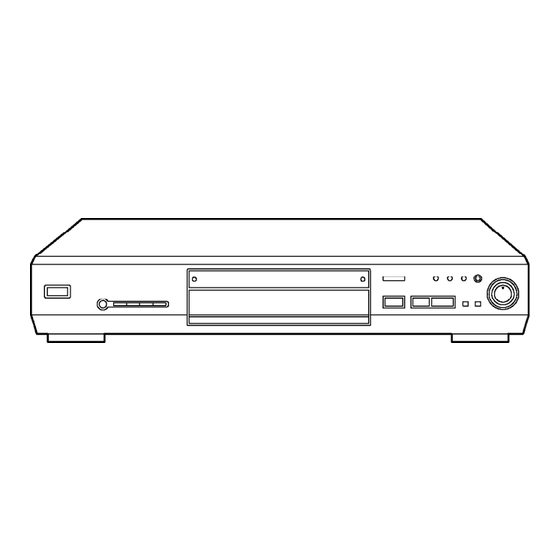
Summary of Contents for Panasonic DVD-RV22PP
- Page 1 ORDER NO. ODSD020318A1 DVD Player DVD-RV22PP Colour (K).....Black Type Please use this manual together with the service manual for Model No.DVD-RV32P, Order No.ODSD020112C1. SPECIFICATIONS Specifications...
- Page 2 Power supply: AC120 V, 60 Hz 14 W Power consumption: Dimensions: 430 (W)×247 (D)×74.5 (H) [1615/16”(W) x 912/16”(D) x 2 15/ 16” (H)] (excluding protrusions) Mass: 2.4 kg (5.31 lb.) Signal system: NTSC Operating temperature range: +5 to +35°C (+41 to 95°F) Operating humidity range: 5 to 90 % RH (no condensation)
- Page 3 sampling) 4 Hz-20 kHz CD audio: (2) S/N ratio: 115 dB CD audio: (3) Dynamic range: 102 dB DVD (linear audio): 98 dB CD audio: (4) Total harmonic distortion: 0.0025 % CD audio: Digital audio output: Optical digital output: Optical terminal Pickup Wave length: 658 nm/790 nm...
- Page 4 1.1. Change in Replacement Parts List Mentioned in the parts list is only those different from Model No. DVD-RV32P Ref. No. Change of Part NO. Part Name & Description Remarks DVD-RV32P DVD-RV22PP CABINET AND CHASSIS REP3303C REP3303T MODULE P.C.B. REP3304C REP3304N MOTHER P.C.B.
-
Page 5: Print Circuit Board
Ref. No. Change of Part NO. Part Name & Description Remarks DVD-RV32P DVD-RV22PP R6026 ERJ3GEYJ272V ERJ3GEYJ472V 1/16W 4.7K RESISTOR-RESISTOR RA4001 EXBV4V473JV ---- RESISTOR-RESISITOR Deletion RA4002 EXBV8V104JV ---- RESISTOR-RESISITOR Deletion RA4003 EXBV4VR000V ---- RESISTOR-RESISITOR Deletion RA4004 EXBV8VR000V ---- RESISTOR-RESISITOR Deletion RA4005,06... - Page 6 C6511 C3210 R3201 TC2037 CP4201 C4202 R3204 C6512 TC2039 K6252 TC2041 R3302 TC2043 C3215 LB4214 LB4213 TC4212 C4211 K6251 CP4202 TC4211 TC3209 TC3208 TC3207 CP4203 QR3301 IC4211 LB4200 CP4204 PS4201 PS3201 C4212 TC3205 K3301 (FOIL SIDE) DVD-RV22PP MODULE P.C.B. REP3303T...
- Page 7 PO SECTION:Page VO SECTION:Page AO SECTION:Page OP SECTION:Page NODC SECTION:Page AVDEC SECTION:Page AD SECTION:Page CPU SECTION:Page VD SECTION:Page DVD-RV22PP AUDIO-DAC SECTION (MODULE P.C.B.(4/6)) SCHEMATIC DIAGRAM...
- Page 8 PO SECTION:Page VO SECTION:Page AO SECTION:Page OP SECTION:Page NODC SECTION:Page AVDEC SECTION:Page CPU SECTION:Page VD SECTION:Page AD SECTION:Page DVD-RV22PP AVDEC SECTION (MODULE P.C.B.(2/6)) SCHEMATIC DIAGRAM...
- Page 9 PO SECTION:Page VO SECTION:Page AO SECTION:Page OP SECTION:Page NODC SECTION:Page AVDEC SECTION:Page AD SECTION:Page CPU SECTION:Page VD SECTION:Page DVD-RV22PP CPU SECTION (MODULE P.C.B.(6/6)) SCHEMATIC DIAGRAM...
- Page 10 2 SCHEMATIC DIAGRAM 2.1. AVDEC SECTION (MODULE P.C.B. (2/6)) SCHEMATIC DIAGRAM...
- Page 11 PO SECTION:Page VO SECTION:Page AO SECTION:Page OP SECTION:Page AVDEC SECTION:Page NODC SECTION:Page CPU SECTION:Page AD SECTION:Page VD SECTION:Page DVD-RV22PP AVDEC SECTION (MODULE P.C.B.(2/6)) SCHEMATIC DIAGRAM...
- Page 12 2.2. AUDIO-DAC SECTION (MODULE P.C.B. (4/6)) SCHEMATIC DIAGRAM PO SECTION:Page VO SECTION:Page AO SECTION:Page OP SECTION:Page NODC SECTION:Page AVDEC SECTION:Page AD SECTION:Page CPU SECTION:Page VD SECTION:Page...
- Page 13 DVD-RV22PP AUDIO-DAC SECTION (MODULE P.C.B.(4/6)) SCHEMATIC DIAGRAM...
- Page 14 2.3. CPU SECTION (MODULE P.C.B. (6/6)) SCHEMATIC DIAGRAM PO SECTION:Page VO SECTION:Page AO SECTION:Page OP SECTION:Page NODC SECTION:Page AVDEC SECTION:Page AD SECTION:Page CPU SECTION:Page VD SECTION:Page...
- Page 15 DVD-RV22PP CPU SECTION (MODULE P.C.B.(6/6)) SCHEMATIC DIAGRAM...
- Page 16 L4201 C4201 C4206 IC3201 C3303 LB2042 LB2043 IC3301 X6501 IC6251 C3302 C4218 C4222 K4201 TP4276 LB4212 LB4211 TP4282 TP3277 TP4285 TP6272 TP6275 TP6277 TP6273 TP6279 TP6271 TP6274 TP6276 TP6278 TC6230 C4216 FP3202 FP3203 FP4202 (COMPONENT SIDE) DVD-RV22PP MODULE P.C.B. REP3303T...
- Page 17 ORDER NO.ODSD020112C1 DVD Player DVD-RV32P-CHINA-PRODUCT / DVD-RV32PC-CHINA- PRODUCT Colour (K).......Black Type (S).......Silver Type Note: DVD-RV32 has Japanese production and the China production. A part for China production is carried to this Service Manual. Please refer to “1. FOR DISTINCTION OF PRODUCT FACTORY.”...
- Page 18 Power supply: AC120 V, 60 Hz 14 W Power consumption: Dimensions: 430 (W)×247 (D)×74.5 (H) [1615 /16 ”(W) x 912 /16 ”(D) x 215 /16 ” (H)] (excludingprotrusions) Mass: 2.4 kg (5.31 lb.) Signal system: NTSC Operating temperature range: +5 to +35°C (+41 to 95°F) Operating humidity range: 5 to 90 % RH (no condensation)
- Page 19 4 Hz-22 kHz (48 kHz DVD (linear audio): sampling) 4 Hz-44 kHz (96 kHz sampling) 4 Hz-20 kHz CD audio: (2) S/N ratio: 115 dB CD audio: (3) Dynamic range: 102 dB DVD (linear audio): 98 dB CD audio: (4) Total harmonic distortion: 0.0025 % CD audio: Digital audio output:...
-
Page 20: Safety Precautions
2. SAFETY PRECAUTIONS 2.1. GENERAL GUIDELINES 1. When servicing, observe the original lead dress. If a short circuit is found, replace all parts which have been overheated or damaged by the short circuit. 2. After servicing, see to it that all the protective devices such as insulation barriers, insulation papers shields are properly installed. -
Page 21: Prevention Of Electro Static Discharge
When the exposed metallic part has a return path to thechassis, the reading should be between 1M and 5.2M . / When the exposed metal does not have a return path to the chassis, the reading must be . Figure 1 2.1.2. - Page 22 components commonly are called Electrostatically Sensitive (ES) Devices. Examples of typical ES devices are integrated circuits and some field-effect transistorsand semiconductor "chip" components. The following techniques should be used to help reduce the incidence of component damage caused by electro static discharge (ESD). 1.
-
Page 23: Precaution Of Laser Diode
carpeted floor can generate static electricity (ESD) sufficient todamage an ES device). 4. Precaution of Laser Diode 5. General Description 5.1. Operating instructions 6. Disassembling the Casing and Checking P.C.B.s 6.1. Dissasembly Procedure... - Page 24 6.2. Caseing Parts and P.C.B. Positions 6.3. Top Cover 1. Unscrew the screws.
- Page 25 6.4. Tray 1. Pull the tray out of the mechanism unit. Remove the gear and install it onto a screwdriver to make a gear jig. 2. Insert the gear jig into the tray open/close hole. 3. Turn the gear jig counterclockwise to open the tray. 4.
- Page 26 6.5. Front Panel 1. Release the tabs. 2. Remove the connectors. 6.6. Mechanism Unit 1. Unscrew the screws. 2. Remove the connectors. 3. Pull out the mechanism unit vertically.
- Page 27 6.7. Terminal P.C.B. 1. Unscrew the screws. 2. Remove the solders. 3. Remove the connectors. 6.8. Module P.C.B. 1. Unscrew the screws. 2. Remove the connectors. 3. Press each tab with the nipper to pull out the module PCB vertically.
- Page 28 6.9. Front-1 P.C.B. and Front-2 P.C.B. 1. Unscrew the screws. 2. Release the tabs. 6.10. Rear panel 1. Unscrew the screws 2. Release the tabs.
-
Page 29: Servicing Position
6.11. Mother P.C.B. 1. Unscrew the screws. 6.12. Servicing Position 6.12.1. Servicing position of the Module P.C.B. -
Page 30: Prevention Of Static Electricity Discharge
6.12.2. Servicing position of the Terminal P.C.B. 6.12.3. List of the Extention Cables 7. PREVENTION OF STATIC ELECTRICITY DISCHARGE The laser diode in the traverse unit (optical pickup) may brake down due to static electricity of clothes or human body. Use due caution to electrostatic breakdown when servicing and handling the laser diode. - Page 31 7.1.2. Human body grounding 1. Use the anti-static wrist strap to discharge the static electricity form your body. 7.1.3. Handling of optical pickup 1. To keep the good quality of the optical pickup maintenance parts during transportation and before installation, the both ends of the laser diode are short-circuited.
-
Page 32: Replacement Procedure
REPLACEMENT PROCEDURE 8.1. Self-diagnosis The optical pickup self-diagnosis function and tilt adjustment check function have been included in this unit. When repairing, use the following procedure for effective Self-diagnosis and tilt adjustment.Be sure to use the self-diagnosis functionbefore replacing the optical pickup when "NO DISC"... - Page 33 and Spindle Motor Assembly Before replacing the optical pickup unit and spindle motor assembly, check the total using hours for each of them. The checking method is as follows: Cautions to be taken when replacing the optical pickup The optical pickup may break down due to the static electricity of human body. Take proper protection measures against static electricity before repairing the parts around the optical pickup.
-
Page 34: Self-Diagnosis Function And Service Modes
9. Self-Diagnosis Function and Service Modes 9.1. New servicing method for DVD player (5th generation models) With the 5th generation models new self-diagnosis function and new servicing method described below are additionally available. 9.1.1. Firmware updating and recovery with disc - Recovery - Firmware updating Simply run the recovery disc. - Page 35 9.1.2. New self-diagnosis function - Cumulative operation time display function (Spindle motor and DVD /CD laser) - Servo process display function - ADSC internal RAM display function - Other: Increased number of last errors storage 1event 20 events Utilization of the above functions, in combination with servicing procedures, is expected to contribute to higher efficiency of fault diagnosis.
- Page 36 9.2.2. Updating firmware 1. Load the recovery disc RFKZD5TR006 on to the player and run it. 2. Firmware version of the player is automatically checked. Appropriate message appears whenever necessary. 3. Using remote controller's cursor key, select whether version updating is to be done or not. (Selection of Yes/No) 4.
- Page 37 time is displayed. When servicing, check the timer display and use it as information for fault diagnosis. At the time of repair and replacement of these components, make sure to check the operation time and reset the timer after replacement. Operation time of the replacement parts (spindle motor and laser) is the valuable information as actual data for future product quality.
- Page 38 Spindle motor operation time ..In STOP mode, main unit PAUSE +FWD-SKIP+ remote controller [6] To reset the timer, perform the following while displaying the time with above key operation. Laser operation time ..... In STOP mode, main unit STOP+FWD -SKIP+ remote controller [5] Spindle motor operation time ..
- Page 39 When focus gain remains at initial value and tracking gain changes, fault exists before ADSC input. When focus gain changes and tracking gain remains at initial value, fault exists after ADSC output. [Tracking system] When focus gain remains at initial value and tracking gain changes, fault exists after ADSC output.
-
Page 40: Service Mode Table
2 digits, normally 06, are ignored.) Picking up servo learned value (Determined) 1. Focus (primary)/tracking balance learning ... When leading in focus 2. Focus/tracking gain and equalizer ... When leading in tracking 3. Focus balance (secondary) ... When leading in tacking [Note] When fault exists somewhere after tracking servo, the disc type is switched by retry to make learned value different from the one in normal startup. -
Page 41: Dvd Self Diagnostic Function-Error Code
Player buttons Remote control unit Application Note buttons PAUSE / + / Displaying the UHF display F_ _ _ Refer to OPEN/CLOSE 9.6. Self- Diagnosis Function Display). Jitter check, tilt adjustment Refer to 11.4. Optical *Display shows J_xxx_yyy_zz Pickup Tilt "yyy"... - Page 42 Error Error Content Additional error explanation Defect 1 Defect 2 Defect 3 Code U, H error Focus error Tray loading error Spindle servo (Spindle servo, DSC SP motor, CLV error servo error) Traverse servo error Tracking servo error Seek error Power error Cannot switch off the power because of the panel and system...
- Page 43 Error Error Content Additional error explanation Defect 1 Defect 2 Defect 3 Code F603 Access failure to Access failure to CSS data of disc KEYDET caused by demodulation error F610 ODC abnormality No permission for command execution F611 6626 QCODE Access failure to seek address in CD don’t read Error series...
-
Page 44: Last Error Code Saved During No Play
Error Error Content Additional error explanation Defect 1 Defect 2 Defect 3 Code F893 FROM FROM falsification F894 EEPROM EEPROM Serial / abnormality communication on lone F8A0 Message Begin sending message to AV task command is not appropriate 9.7. Last Error Code saved during NO PLAY Error Error Content System computer... - Page 45 9.9. Service mode table 2 Pressing various button combinations on the player and remote control unit can activate the service modes.
-
Page 47: Servo Process Flow
9.10. Servo Process Flow... -
Page 48: Servo Process Display Mode
9.11. Servo Process Display Mode 9.12. Sales demonstration lock function This function prevents discs from being lost when the unit is used for sales demonstrations by disabling the disc eject function. "LOCKED" is displayed on the unit, and ordinary operation is disabled. -
Page 49: Assembling And Disassembling The Mechanism Unit
9.12.2. Cancellation The lock can be cancelled by the same procedure as used in setting. ("UNLOCKED" is displayed on cancellation. Disconnecting the power cable from power outlet does not cancel the lock.) 9.13. Service Precautions 9.13.1. Recovery after the dvd player is repaired 9.13.2. - Page 50 10.2. Terminal P.C.B. 1. Unscrew the screws. 2. Remove the solders. 3. Remove the connectors.
- Page 51 10.3. Clamp Plate Unit 1. Spread the stopper with hand to slide the tabs and remove the clamp plate unit. 10.4. Tray 1. Lift the tray.
- Page 52 Reassemble the tray so that it is in the backmost position. 1. Turn traverse gear until cam gear leaver comes to the lever adjusting position at the end of mechanical chassis unit. 2. Check the position of convex phase on back of the tray, and that of concave phase on drive gear.
- Page 53 A. Place the tray on the unit from rearward. B. Inch the tray frontward until convex phase and concave phase mate.
- Page 54 Caution: Make sure to mate convex phase and concave phase properly, so that the gap between turntable and tray becomes 5mm or less. 10.5. Traverse Block 1. Lift the traverse block while spreading the hook of the mechanical chassis unit. 2.
- Page 55 10.6. Traverse Gear 1. Disengage the tabs from the traverse gear. 2. Remove the traverse gears B and C.
- Page 56 10.7. Optical Pickup Unit 1. Unscrew the screws. 2. Remove the spring holders and the springs. 3. Pull out the drive shaft and guide shaft.
- Page 57 10.7.1. Precautions in optical pickup replacement The optical pickup can be damaged by static electricity from you body. Be sure to take static electricity countermeasures when working around the optical pickup. (Refer to the related page in this Manual about the countermeasures.) 1.
- Page 58 10.7.2. Disassembling the Optical Pickup Unit 1. Remove the 2 screws A and remove the TRV feed rack. 2. Remove the screw B and remove the Terminal FPC. 3. Remove the optical pickup. Fig. 1...
- Page 59 10.7.3. Cautions to Be Taken When Replacing the Optical Pickup - An antistatic flexible sheet (FPC) is connected with the new optical pickup. Replace the optical pickup according to the following procedure. 1. Install the Terminal FPC, TRV feed rack on the optical pickup. (See Fig.
- Page 60 3. Install the optical pickup unit, spring, drive shaft, guide shaft, rubber cushion, and spring holder on the traverse block. Fig. 3...
- Page 61 Cautions to be taken when assembling the unit: Install the pickup unit so that it is located at the rear end of the guide shaft.) 4. Cut the antistatic flexible sheet for the optical pickup unit. Fig. 4...
- Page 62 10.8. Disassembling the Middle Chassis 1. Remove the holder pins. 2. Remove the tab. 3. It lifts while pulling it in the direction of the arrow.
- Page 63 10.9. Disassembling the Traverse Gear A 1. Unscrew the screw. 2. Remove the traverse gear A. 10.10. Disassembling the Spindle Motor Unit 1. Remove the floating rubbers.
-
Page 64: Adjustment Procedures
11. ADJUSTMENT PROCEDURES 11.1. Service Tools and Equipment Application Name Number Tilt adjustment DVD test disc DVDT-S15 or DVDT-S01 Hex wrench Available on sales route. Inspection Extension cable (module P.C.B. to mother JGS0116 P.C.B.) Extension cable (module P.C.B. to mother VUC8026 P.C.B.) Others... -
Page 65: Optical Adjustment
- Surface precision is vital for DVD test discs. Be sure to store and handle them carefully. 1. Do not place discs directly onto the workbench, etc., after use. 2. Handle discs carefully in order to maintain their flatness. Place them into their case after use and store them vertically. - Page 66 5. Play test disc T43 (outer periphery). 6. Adjust tilt adjustment screw 1 so that the jitter value is minimized. 7. Play test disc T43 (outer periphery). 8. Adjust tilt adjustment screw 2 so that the jitter value is minimized. 9.
- Page 67 screw in position using screw lock. 11.4.1.4. Procedure for screw lock 1. After adjustment, remove top cover, tray, clamper base and traverse unit in this sequence. 2. Lay the traverse unit upside down, and fix adjustment screw with screw lock. 3.
- Page 68 INITIAL/LOGO ABBREVIATIONS A0~UP ADDRESS ACLK AUDIO CLOCK AD0~UP ADDRESS BUS ADATA AUDIO PES PACKET DATA ADDRESS LATCH ENABLE AMUTE AUDIO MUTE AREQ AUDIO PES PACKET REQUEST AUDIO RF SERVO AMP INVERTED INPUT SERVO AMPOUTPUT ASYNC AUDIO WORD DISTINCTION SYNC BIT CLOCK (PCM) BCKIN BIT CLOCK INPUT BLACK DROP OUT...
- Page 69 INITIAL/LOGO ABBREVIATIONS DACCK D/A CONVERTER CLOCK DEEMP DEEMPHASIS BIT ON/OFF DEMPH DEEMPHASIS SWITCHING DIG0~UP FL DIGIT OUTPUT DATA INPUT DMSRCK DM SERIAL DATA READ CLOCK DMUTE DIGITAL MUTE CONTROL DROP OUT DOUT0~UP DATAOUTPUT DATA SLICE RF (BIAS) DROP OUT SIGNAL DRPOUT DATA REQUEST DREQ...
- Page 70 INITIAL/LOGO ABBREVIATIONS IECOUT IEC958 FORMAT DATA OUTPUT IPFRAG INTERPOLATION FLAG IREF I (CURRENT) REFERENCE ISEL INTERFACE MODE SELECT LDON LASER DIODE CONTROL LASER POWER CONTROL LRCK L CH/R CH DISTINCTION CLOCK MA0~UP MEMORY ADDRESS MEMORY CLOCK MCKI MEMORY CLOCK INPUT MCLK MEMORY SERIAL COMMAND CLOCK...
- Page 71 INITIAL/LOGO ABBREVIATIONS READ ENABLE RFENV RF ENVELOPE RF PHASE DIFFERENCE OUTPUT (CD-ROM) REGISTER SELECT RSEL RF POLARITY SELECT RESET RESERVE SBI0, 1 SERIAL DATA INPUT SBO0 SERIAL DATA OUTPUT SBT0, 1 SERIAL CLOCK SERIAL DATA CLOCK SCKR AUDIO SERIAL CLOCK RECEIVER SERIAL CLOCK SCLK...
- Page 72 SUB CODE Q DATA SYSCLK SYSTEM CLOCK INITIAL/LOGO ABBREVIATIONS TRACKING ERROR TIBAL BALANCE CONTROL BALANCE OUTPUT 1 BALANCE INPUT BALANCE INPUT BALANCE OUTPUT 2 TPSN OP AMP INPUT TPSO OP AMP OUTPUT TPSP OP AMP INVERTED INPUT TRCRS TRACK CROSSSIGNAL TRON TRACKING ON TRSON...
-
Page 73: Voltage Chart
INITIAL/LOGO ABBREVIATIONS X' TAL XALE X ADDRESS LATCH ENABLE XAREQ X AUDIO DATA REQUEST XCDROM X CD ROM CHIP SELECT X CHIP SELECT XCSYNC X COMPOSITE SYNC X DATA STROBE XHSYNCO X HORIZONTAL SYNC OUTPUT XHINT XH INTERRUPTREQUEST X' TAL OSCILLATOR INPUT XINT X INTERRUPT X MEMORY WRITE ENABLE... -
Page 74: Schematic Diagram
15. SCHEMATIC DIAGRAM 15.1. INTERCONNECTION SCHEMATIC DIAGRAM 15.2. POWER SECTION (MOTHER P.C.B. (1/4)) SCHEMATIC DIAGRAM 15.3. VIDEO-OUT SECTION (MOTHER P.C.B. (2/4)) SCHEMATIC DIAGRAM 15.4. AUDIO-OUT SECTION (MOTHER P.C.B. (3/4)) SCHEMATIC DIAGRAM 15.5. OPERATION & FL SECTION (MOTHER P.C.B. (4/4)) SCHEMATIC DIAGRAM 15.6. -
Page 75: Exploded Views
17. EXPLODED VIEWS 17.1. Casing Parts & Mechanism Section Exploded View 17.2. Mechanism Section Exploded View... -
Page 76: Packing & Accessories Section Exploded View
17.3. Packing & Accessories Section Exploded View... -
Page 77: Replacement Parts List
18. REPLACEMENT PARTS LIST Notes: *Important safety notice: Components identified by mark have special characteristics important for safety. Furthermore, special parts which have purposes of fire-retardant (resistors), high-quality sound (capacitors), low-noise (resistors), etc. are used. When replacing any of components, be sure to use only manufactures specified parts shown in the parts list. - Page 78 SCREW RHDC0001 SCREW REZ1355 FLEXIBLE CABLE(50P) REX1057 CONNECTOR CABLE(2P) CYP0003-K FRONT PANEL ASS’Y 2 CYP0003-S FRONT PANEL ASS’Y2 16-1 VGB0298 PANASONIC BADGE CEP0005AA FRONT1 P.C.B. (RTL) XTBS26+10J SCREW RXQ0755 SHUTTLE BASE ASS’Y CGW0001-K SHUTTLE KNOB CGW0001-S SHUTTLE KNOB CMC0001 EARTH PLATE A...
- Page 79 Ref. No. Part No. Part Name & Description Remarks RMSC0710 DRIVE SHAFT RMSC0711 GUIDE SHAFT RHD17036 SCREW VHD1224 SCREW RDG0500 TRAVERSE GEAR(B) RDG0501 TRAVERSE GEAR(C) RMEC0319 TRAVERSE GEAR SPRING RGQ0280-K3 TRAY RXQ0748 MECHA CHASSIS ASS’Y 129-1 XTW3+12S SCREW 129-2 RSH1A049-U OPEN SWITCH K0F111E00093 RME0318...
- Page 80 Ref. No. Part No. Part Name & Description Remarks C1141 ECA1HM330B 50V 33U C1142 ECUV1E104ZFV 25V 0.1U F1H1E104A030 C1143 ECA1CM100B 16V 10U C1151 VCEA1EJH271B 25V 270U F2A1E2710001 C1153 ECA1EM331B 25V 330U C1154 ECA1CM221 16V 220U C1161 VCEA1HJH560B 50V 560 F2A1H5600002 C1171 VCEA1AJH181B 10V 180U...
- Page 81 Ref. No. Part No. Part Name & Description Remarks C3017,18 ECUX1C104ZFV 16V 0.1U C3019,20 ECUV1A105ZFV 10V 1U F1H1A1050002 C3021-23 ECUX1C104ZFV 16V 0.1U C3024 ECUV1A105ZFV 10V 1U F1H1A1050002 C3025 ECUX1C104ZFV 16V 0.1U C3026 ECUV1A105ZFV 10V 1U F1H1A1050002 C3027-29 ECUX1C104ZFV 16V 0.1U C3030 ECUV1A105ZFV 10V 1U...
- Page 82 Ref. No. Part No. Part Name & Description Remarks C4381 ECUV1C223KBV 16V 0.022U ECJ1VB1C223K C4382,83 ECUV1E104ZFV 25V 0.1U F1H1E104A030 C4385 ECUV1C223KBV 16V 0.022U ECJ1VB1C223K C4391 ECUV1E104ZFV 25V 0.1U F1H1E104A030 C4401-07 ECUV1E104ZFV 25V 0.1U F1H1E104A030 C4411 ECA1CAK470XB 16V 47U C4412 ECUX1H102JCV 50V 1000P C4421 ECA1CAK470XB...
- Page 83 Ref. No. Part No. Part Name & Description Remarks C6501,02 EEVHB0J330R 6.3V 33U C6503-05 ECUX1C104ZFV 16V 0.1U C6511,12 ECUX1H150JCV 50V 15P ECJ1VC1H150J D1001 ENC471D5ATUB DIODE D4EA7471A001 D1002 ENC361D5ATRB DIODE D4EA7361A002 D1011 B0EBKT000002 DIODE D1031 VSD0002 DIODE B0HAGR000005 D1041 AU01Z DIODE B0HAGM000006 D1051,52 MA165...
- Page 84 Ref. No. Part No. Part Name & Description Remarks IC4031 C0JBAR000294 IC4041 AHC1G08HDCK C0JBAA000260 IC4051 AHC1G08HDCK C0JBAA000260 IC4061 AHC2G74HDCTR C0JBAF000367 IC4201 C0FBBK000030 IC4311 C0ABBB000118 IC4381 C0ABBB000118 IC5201 AN8708FHK-V IC6001 MN101C35DCM IC6011 C0EBE0000106 IC6101 B3RAD0000037 IC6201 MN102H60GFC IC6251 C0DBCGE00002 IC6301 PST596JNR C0EBE0000070 IC6302 RFKFRV62B080...
- Page 85 Ref. No. Part No. Part Name & Description Remarks LB2001 J0JHC0000045 COIL LB2011-41 VLP0146-T COIL J0JBC0000015 LB2042,43 J0JHC0000045 COIL LB3001,02 J0JHC0000045 COIL LB3011 VLP0157-T COIL J0JCC0000077 LB3201 VLP0155-T COIL J0JCC0000119 LB3202-04 ERJ3GEYJ101V 1/16W 100 LB3206-08 VLP0155-T COIL J0JCC0000119 LB3533,34 VLP0146-T COIL J0JBC0000015 LB3536-39...
- Page 86 Q1115 B1DHCC000029 TRANSISTOR...
- Page 87 Ref. No. Part No. Part Name & Description Remarks Q1125 2SB1417PQTA TRANSISTOR 2SB14170JA Q1126 XN1501TX TRANSISTOR XN0150100L Q1141 2SB1320A-RTA TRANSISTOR 2SB1320ARA Q4392 2SD601A-RSTX TRANSISTOR 2SD0601AHL Q4411 2SD1328-R TRANSISTOR 2SD13280R Q4421 2SD1328-R TRANSISTOR 2SD13280R Q4481-83 2SD601A-RSTX TRANSISTOR 2SD0601AHL Q5211 2SB1115-T TRANSISTOR B1BDBF000004 Q5215 2SB1115-T...
- Page 88 Ref. No. Part No. Part Name & Description Remarks R2021 ERJ3GEYJ332V 1/16W 3.3K D0GB332JA002 R2022 ERJ3GEYJ123V 1/16W 12K R2023 ERJ3GEYJ332V 1/16W 3.3K D0GB332JA002 R2024 ERJ3GEYJ123V 1/16W 12K R2026 ERJ3GEYJ473V 1/16W 47K D0GB473JA002 R2028,29 ERJ3GEYJ472V 1/16W 4.7K R2030 ERJ3GEYJ103V 1/16W 10K D0GB103JA002 R2031-33 ERJ3GEYJ682V...
- Page 89 Ref. No. Part No. Part Name & Description Remarks R4313 JAR0816P123D 1/16W 12K D0HB123ZA002 R4321 ERJ3GEYJ104V 1/16W 100K D0GB104JA002 R4322 JAR0816P562D 1/16W 5.6K D0HB562ZA002 R4323 JAR0816P123D 1/16W 12K D0HB123ZA002 R4381,82 ERJ3GEYJ683V 1/16W 86K D0GB683JA002 R4383 ERJ3GEYJ473V 1/16W 47K D0GB473JA002 R4385 ERJ3GEYJ333V 1/16W 33K D0GB333JA002...
- Page 90 Ref. No. Part No. Part Name & Description Remarks R6095 ERJ3GEYJ103V 1/16W 10K D0GB103JA002 R6161 ERDS2FJ122 1/4W 1.2K ERDS2TJ122T R6162 ERDS2FJ152 1/4W 1.5K R6171 ERDS2FJ122 1/4W 1.2K ERDS2TJ122T R6172 ERDS2FJ152 1/4W 1.5K R6173 ERDS2FJ222 1/4W 2.2K ERDS2TJ222T R6174 ERDS2FJ332 1/4W 3.3K R6175 ERDS2FJ472 1/4W 4.7K...
-
Page 91: Schematic Diagram For Printing With A4 Size
Ref. No. Part No. Part Name & Description Remarks S6175 EVQ11G07K SWITCH(REPEAT) S6176 EVQ11G07K SWITCH(RANDOM) S6181 EVQ11G07K SWITCH(OPEN/CLOSE) S6191 ESE24SH7 SWITCH(COUNT) S6192 ESE24SH7 SWITCH(DIRECTION) SW2501 RSH1A048-A DOUBLE SWITCH T1021 ETS28AV145AC TRANSFORMER X6001 RSXY8M00M06T CERAMIC OSCILLATOR H2D800400009 X6501 VSX1044 CRYSTAL OSCILLATOR H0J368500003 19. - Page 92 FRONT 2 P.C.B. R6177 R6181 R6180 R6179 R6178 DIALOGUE ADVANCED POWER IC6101 ENHANCER CINEMA BASS PLUS SURROUND S6101 ONE TOUCH S6106 S6105 S6104 S6103 CINEMA DISP S6102 D6103 C6101 PP6001 R6176 SLEEP LED FRONT 1 P.C.B. QUICK-REPLAY A-B/REPEAT REPEAT RANDOM OPEN/CLOSE S6173 S6174...
- Page 93 MODULE P.C.B. (1/2) TL6202 TL6207 TL6208 TL6205 TL6204 TL6203 TL6209 TL6206 TL6210 PS6201 TL6201 LB3002 R6206 K6301 C3002 C3001 K6201 CP6231 CP6213 RA6207 D6201 CP6232 CP6221 C3020 C3019 C3018 C3017 C3016 C3015 C6203 K3013 R6205 LB6202 CP6222 C6303 C6202 C3014 IC6221 CP6225 CP6224...
- Page 94 MODULE P.C.B. (2/2) TP6205 TP6208 TP6207 TP6202 TP6201 LB3001 TP6210 TP6206 TP6209 TP6203 TP6204 R6301 CP3004 C6306 TC6201 CP3002 CP3006 CP3001 CP3007 CP3003 CP3008 CP3005 RA3008 CP3010 CP3009 CP6312 CP6313 IC6302 C6212 C3060 C3021 CP6226 CP6235 CP6237 CP6328 CP6208 C3022 CP6329 CP6322 CP6321...
- Page 95 MOTHER P.C.B. TC6059 TC6021 TC6042 DL6001 TC6054 TC6055 TC6058 TC6002 TC6048 TC6056 TC6063 TC6053 LB6021 TC6046 TC6049 TC6060 TC6064 TC6068 PS6003 PS6001 TC6044 TC6050 TC6052 TC6062 PS6002 TC6005 R6083 TC6070 TC6024 TC6047 TC6051 TC6061 TC6066 TC6041 TC6045 R6048 TC6071 R6082 TC6065 TC6069 LB6002...
- Page 96 TERMINAL P.C.B. FP5201 LB5206 C5251 C5223 QR5251 C5201 L5251 Q5215 C5253 C5231 L5202 LB5202 LB5205 R5252 R5213 IC5201 R5214 R5204 R5216 R5217 Q5211 R5232 R5212 R5211 R5236 C5203 SW2501 R5235 C5240 C2507 R2503 R2502 R2505 R2504 C2513 M2502 C2505 IC2501 M2501 C2508 R2506...
- Page 97 PO SECTION:Page VO SECTION:Page AO SECTION:Page OP SECTION:Page NODC SECTION:Page AVDEC SECTION:Page AD SECTION:Page VD SECTION:Page WMA SECTION:Page CPU SECTION:Page DVD-RV32P/PC AUDIO-DAC SECTION (MODULE P.C.B.(4/6)) SCHEMATIC DIAGRAM...
- Page 98 MAIN SIGNAL IC3001 IC4201 (AV DECODER) (AUDIO D/A CONVERTER) JK4401 IC4311 MIXL OUTPUT AMP MIX L AUDIO LRCK SERIAL DATA LOW-PASS PORT FILTER OVERSAMPLING ENHANCED DIGITAL FILTER A MUT FROM MULTI-LEVEL IC6201-64PIN WITH STBDAC DELTA-SIGMA FROM FUNCTION MODULATOR IC6201-57PIN CONTROLLER SERIAL IC4311 SBT1...
- Page 99 PO SECTION:Page VO SECTION:Page AO SECTION:Page OP SECTION:Page NODC SECTION:Page AVDEC SECTION:Page AD SECTION:Page VD SECTION:Page WMA SECTION:Page CPU SECTION:Page DVD-RV32P/PC AUDIO-OUT SECTION (MOTHER P.C.B.(3/4)) SCHEMATIC DIAGRAM...
- Page 100 PO SECTION:Page VO SECTION:Page AO SECTION:Page OP SECTION:Page NODC SECTION:Page AVDEC SECTION:Page VD SECTION:Page AD SECTION:Page WMA SECTION:Page CPU SECTION:Page DVD-RV32P/PC AVDEC SECTION (MODULE P.C.B.(2/6)) SCHEMATIC DIAGRAM...
- Page 101 PO SECTION:Page VO SECTION:Page AO SECTION:Page OP SECTION:Page NODC SECTION:Page AVDEC SECTION:Page AD SECTION:Page VD SECTION:Page WMA SECTION:Page CPU SECTION:Page DVD-RV32P/PC CPU SECTION (MODULE P.C.B.(6/6)) SCHEMATIC DIAGRAM...
- Page 102 DVD-RV32P/PC FRONT1,FRONT2 SCHEMATIC DIAGRAM...
- Page 103 FP5202 FP2001 TERMINAL P.C.B. A GND A GND HFMON HFMON GAIN H/L GAIN H/L A GND A GND F BAL F BAL T BAL T BAL A GND A GND FEP ENB FEP ENB FEP CLK FEP CLK OPTICAL FEP DATA FEP DATA OFTR OFTR...
- Page 104 MODULE P.C.B. Transistor CP4021 D-5 C CP6319 F-4 C TC3303 A-5 F TP4008 D-5 C Q3101 C-2 F CP4022 D-5 C CP6320 E-5 F TC3304 A-5 F TP4271 A-4 C Q3106 C-3 F CP4023 D-4 C CP6321 E-5 F TC3305 A-6 F TP4272 A-4 C...
- Page 105 MOTHER P.C.B. Transistor Integrated Circuit TC6051 TL1118 Q1021 IC1101 TC6052 TL4301 Q1051 IC1151 TC6053 TL4302 Q1052 IC3501 TC6054 TL4311 Q1062 IC4311 TC6055 TL4312 Q1115 IC4381 TC6057 TL4481 Q1125 IC6001 TC6058 TL4482 Q1126 IC6011 TC6059 TP1101 Test Point Q1141 TC6060 TP1102 Q1155 TC5056 TC6061...
- Page 106 PO SECTION:Page VO SECTION:Page AO SECTION:Page OP SECTION:Page AVDEC SECTION:Page NODC SECTION:Page AD SECTION:Page VD SECTION:Page WMA SECTION:Page CPU SECTION:Page DVD-RV32P/PC NODC SECTION (MODULE P.C.B.(1/6)) SCHEMATIC DIAGRAM...
- Page 107 PO SECTION:Page VO SECTION:Page AO SECTION:Page OP SECTION:Page NODC SECTION:Page AVDEC SECTION:Page AD SECTION:Page VD SECTION:Page WMA SECTION:Page CPU SECTION:Page DVD-RV32P/PC OPERATION & FL SECTION (MOTHER P.C.B.(4/4)) SCHEMATIC DIAGRAM...
- Page 108 MECHANISM UNIT MODULE P.C.B. MOTHER P.C.B. FEP TERMINAL P.C.B. IC5201 IC2001 IC3001 IC4201 FRONT MIXL OPTICAL AUDIO PICK UP PROCESSOR UNIT CONVERTER MIXR (FEP) IC6501 IC2501 SPINDLE OPTICAL MOTOR DISC MOTOR CONTROLLER IC6302 DRIVE (NODC) TRAVERSE 8Mbit MOTOR FLASH DECODER (AV DEC) IC6201 MAIN...
- Page 109 PRIMARY CIRCUIT SECONDARY CIRCUIT IC6001 D1011 (SUB CPU) L1001 C1011,C1012 T1021 DZ1001 AC SOCKET D1001 NSW+10/+12V AUDIO DGT13 P1001 NSW-10/-12V OP AMPS SURGE D1002 Q1125, DGT1 SUPPRESSOR SURGE LINE & RECTIFIER KILLER FILTER POWER SURGE TRANSFORMER ABSORBER F1001 Q1126 SEG23 REG.
- Page 110 PO SECTION:Page VO SECTION:Page AO SECTION:Page OP SECTION:Page NODC SECTION:Page AVDEC SECTION:Page AD SECTION:Page VD SECTION:Page WMA SECTION:Page CPU SECTION:Page DVD-RV32P/PC POWER SECTION (MOTHER P.C.B.(1/4)) SCHEMATIC DIAGRAM...
- Page 111 IC5201 (FEP) IC2001 OPTICAL PICK UP UNIT (NODC) PEAK VIN7 PHOTO DETECTOR RFENV HOLD VIN8 FBAL HEAD VIN1 COMP. DEFFERENTIAL PHASE DET. VIN2 COMP. VIN3 COMP. TBAL DEFFERENTIAL PHASE DET. VIN4 COMP. VIN5 VIN6 FBAL VIN9 TBAL VIN10 RSCL S LINE VREF LASER DIODE Q5211...
- Page 112 IC2001 RF SIGNAL MOTOR DRIVE SIGNAL TRACKING ERROR SIGNAL FOCUS ERROR SIGNAL (NODC) IC2501 (MOTOR DRIVE) VO4+ M2502 TRAVERS MOTOR LEVEL TRSDRV TRIN VO4- SHIFT BIAS1 OPIN+ TRIN VIN1 VO3+ M2501 SPINDLE MOTOR FOIN VIN2 LEVEL VO3- SHIFT OPIN- SPDIN VIN3 OPOUT FROM...
- Page 113 DVD-RV32P/PC TERMINAL SCHEMATIC DIAGRAM...
- Page 114 PO SECTION:Page VO SECTION:Page AO SECTION:Page OP SECTION:Page AVDEC SECTION:Page NODC SECTION:Page AD SECTION:Page VD SECTION:Page WMA SECTION:Page CPU SECTION:Page DVD-RV32P/PC VIDEO-DAC SECTION (MODULE P.C.B.(3/6)) SCHEMATIC DIAGRAM...
- Page 115 FEP TERMINAL P.C.B. MODULE P.C.B. EUROPE MODEL ONLY IC3071 (16M SDRAM) IC3001-129 IC3001-124 0.68Vp-p(20usec./div.) 0.64Vp-p(20usec./div.) OPTICAL PICK UP UNIT IC3001-134 IC3001-119 MEMORY 1.2Vp-p(20usec/div) 0.8Vp-p(20usec/div) ADDRESS 12bit IC3001-147 TO 150,152 TO 155 6.0Vp-p(20usec./div.) IC5201 IC2001 IC3001 (FEP) (NODC) (AV DECORDER) VIN1 RF ENV RF ENV STD0...
- Page 116 MODULE P.C.B. MOTHER P.C.B. MAIN SIGNAL IC3501-25,30 IC3501-32 IC3501-17,19 2.2Vp-p(20usec./div.) 1.2Vp-p(20usec./div.) 2.2Vp-p(20usec./div.) IC3501 (VIDEO DRIVE) YTRAP YOUT CLAMP MIXOUT VIDEO OUT 1/2 CTRAP COUT 1.5-6M S-VIDEO OUT 1/2 CbTRAP CBIN CBOUT CB/B CRIN CROUT CR/R CrTRAP QR6301 NRST FROM IC6201-79PIN DVD-RV32P/PC DVD-RV32P/PC VIDEO BLOCK DIAGRAM...
- Page 117 PO SECTION:Page VO SECTION:Page AO SECTION:Page OP SECTION:Page NODC SECTION:Page AVDEC SECTION:Page AD SECTION:Page VD SECTION:Page WMA SECTION:Page CPU SECTION:Page DVD-RV32P/PC VIDEO-OUT SECTION (MOTHER P.C.B.(2/4)) SCHEMATIC DIAGRAM...
- Page 118 PO SECTION:Page VO SECTION:Page AO SECTION:Page OP SECTION:Page NODC SECTION:Page AVDEC SECTION:Page VD SECTION:Page AD SECTION:Page WMA SECTION:Page CPU SECTION:Page DVD-RV32P/PC WMA SECTION (MODULE P.C.B.(5/6)) SCHEMATIC DIAGRAM...
- Page 119 15 SCHEMATIC DIAGRAM 15.1. INTERCONNECTION SCHEMATIC DIAGRAM FP5202 TERMINAL P.C.B. A GND HFMON GAIN H/L A GND F BAL T BAL A GND FEP ENB FEP CLK OPTICAL FEP DATA OFTR PICK UP UNIT A GND FP5201 P IN(CD) VHALF T2(CD) A +3.3V FE2(CD)
- Page 120 FP2001 A GND HFMON GAIN H/L A GND F BAL T BAL A GND FEP ENB FEP CLK FEP DATA OFTR A GND VHALF MODULE P.C.B. A +3.3V A +3.3V A GND NARF TST SG RF ENV A +5V V REF2 LD CUR IN SW TRAY/TRV...
- Page 121 15.2. POWER SECTION (MOTHER P.C.B. (1/4)) SCHEMATIC DIAGRAM PO SECTION:Page VO SECTION:Page AO SECTION:Page OP SECTION:Page NODC SECTION:Page AVDEC SECTION:Page AD SECTION:Page VD SECTION:Page WMA SECTION:Page CPU SECTION:Page...
- Page 122 DVD-RV32P/PC POWER SECTION (MOTHER P.C.B.(1/4)) SCHEMATIC DIAGRAM...
- Page 123 15.3. VIDEO-OUT SECTION (MOTHER P.C.B. (2/4)) SCHEMATIC DIAGRAM...
- Page 124 PO SECTION:Page VO SECTION:Page AO SECTION:Page OP SECTION:Page AVDEC SECTION:Page NODC SECTION:Page AD SECTION:Page VD SECTION:Page WMA SECTION:Page CPU SECTION:Page DVD-RV32P/PC VIDEO-OUT SECTION (MOTHER P.C.B.(2/4)) SCHEMATIC DIAGRAM...
- Page 125 15.4. AUDIO-OUT SECTION (MOTHER P.C.B. (3/4)) SCHEMATIC DIAGRAM PO SECTION:Page VO SECTION:Page AO SECTION:Page OP SECTION:Page NODC SECTION:Page AVDEC SECTION:Page AD SECTION:Page VD SECTION:Page WMA SECTION:Page CPU SECTION:Page...
- Page 126 DVD-RV32P/PC AUDIO-OUT SECTION (MOTHER P.C.B.(3/4)) SCHEMATIC DIAGRAM...
- Page 127 15.5. OPERATION & FL SECTION (MOTHER P.C.B. (4/4)) SCHEMATIC DIAGRAM PO SECTION:Page VO SECTION:Page AO SECTION:Page OP SECTION:Page NODC SECTION:Page AVDEC SECTION:Page AD SECTION:Page VD SECTION:Page WMA SECTION:Page CPU SECTION:Page...
- Page 128 AGRAM DVD-RV32P/PC OPERATION & FL SECTION (MOTHER P.C.B.(4/4)) SCHEMATIC DIAGRAM...
- Page 129 15.6. NODC SECTION (MODULE P.C.B. (1/6)) SCHEMATIC DIAGRAM PO SECTION:Page VO SECTION:Page AO SECTION:Page OP SECTION:Page AVDEC SECTION:Page NODC SECTION:Page AD SECTION:Page VD SECTION:Page WMA SECTION:Page CPU SECTION:Page...
- Page 130 DVD-RV32P/PC NODC SECTION (MODULE P.C.B.(1/6)) SCHEMATIC DIAGRAM...
- Page 131 15.7. AVDEC SECTION (MODULE P.C.B. (2/6)) SCHEMATIC DIAGRAM...
- Page 132 PO SECTION:Page VO SECTION:Page AO SECTION:Page OP SECTION:Page NODC SECTION:Page AVDEC SECTION:Page AD SECTION:Page VD SECTION:Page WMA SECTION:Page CPU SECTION:Page DVD-RV32P/PC AVDEC SECTION (MODULE P.C.B.(2/6)) SCHEMATIC DIAGRAM...
- Page 133 15.8. VIDEO-DAC SECTION (MODULE P.C.B. (3/6)) SCHEMATIC DIAGRAM PO SECTION:Page VO SECTION:Page AO SECTION:Page AVDEC SECTION:Page OP SECTION:Page NODC SECTION:Page AD SECTION:Page VD SECTION:Page WMA SECTION:Page CPU SECTION:Page...
- Page 134 DVD-RV32P/PC VIDEO-DAC SECTION (MODULE P.C.B.(3/6)) SCHEMATIC DIAGRAM...
- Page 135 15.9. AUDIO-DAC SECTION (MODULE P.C.B. (4/6)) SCHEMATIC DIAGRAM PO SECTION:Page VO SECTION:Page AO SECTION:Page OP SECTION:Page NODC SECTION:Page AVDEC SECTION:Page AD SECTION:Page VD SECTION:Page WMA SECTION:Page CPU SECTION:Page...
- Page 136 DVD-RV32P/PC AUDIO-DAC SECTION (MODULE P.C.B.(4/6)) SCHEMATIC DIAGRAM...
- Page 137 15.10. WMA SECTION (MODULE P.C.B. (5/6)) SCHEMATIC DIAGRAM PO SECTION:Page VO SECTION:Page AO SECTION:Page AVDEC SECTION:Page OP SECTION:Page NODC SECTION:Page AD SECTION:Page VD SECTION:Page WMA SECTION:Page CPU SECTION:Page...
- Page 138 DVD-RV32P/PC WMA SECTION (MODULE P.C.B.(5/6)) SCHEMATIC DIAGRAM...
- Page 139 15.11. CPU SECTION (MODULE P.C.B. (6/6)) SCHEMATIC DIAGRAM PO SECTION:Page VO SECTION:Page AO SECTION:Page OP SECTION:Page NODC SECTION:Page AVDEC SECTION:Page AD SECTION:Page VD SECTION:Page WMA SECTION:Page CPU SECTION:Page...
- Page 140 DVD-RV32P/PC CPU SECTION (MODULE P.C.B.(6/6)) SCHEMATIC DIAGRAM...
- Page 141 15.12. TERMINAL SCHEMATIC DIAGRAM...
- Page 142 DVD-RV32P/PC TERMINAL SCHEMATIC DIAGRAM...
- Page 143 15.13. FRONT 1 AND FRONT 2 SCHEMATIC DIAGRAM...
- Page 144 DVD-RV32P/PC FRONT1,FRONT2 SCHEMATIC DIAGRAM...
- Page 146 IC2001 Ref No. MODE STOP PLAY IC2001 Ref No. MODE STOP PLAY IC2001 Ref No. MODE STOP PLAY IC2001 Ref No. MODE STOP PLAY IC2001 Ref No. MODE STOP PLAY IC2001 Ref No. MODE STOP PLAY IC2001 Ref No. MODE STOP PLAY IC2001...
- Page 147 IC3001 Ref No. MODE STOP PLAY IC3061 Ref No. MODE STOP PLAY IC3061 Ref No. MODE STOP PLAY IC3061 Ref No. MODE STOP PLAY Ref No. IC4001 MODE STOP PLAY IC4001 Ref No. MODE STOP PLAY IC4001 Ref No. MODE STOP PLAY IC4001...
- Page 148 IC6302 IC6303 Ref No. MODE STOP PLAY IC6501 Ref No. MODE STOP PLAY QR6301 Ref No. MODE STOP PLAY...
- Page 149 IC1101 IC1151 Ref No. MODE STOP 51.7 49.7 52.5 58.0 52.3 57.3 PLAY 51.2 49.6 52.4 58.0 52.4 57.3 IC3501 Ref No. MODE STOP PLAY IC3501 Ref No. MODE STOP PLAY IC4311 IC4381 Ref No. MODE STOP -9.7 -9.7 PLAY -9.7 -9.7 IC6001...
- Page 150 IC6101 Ref No. MODE STOP PLAY...
- Page 151 IC2501 Ref No. MODE STOP PLAY IC2501 Ref No. MODE STOP PLAY IC5201 Ref No. MODE STOP PLAY IC5201 Ref No. MODE STOP PLAY IC5201 Ref No. MODE STOP PLAY Q5211 Q5215 QR5251 Ref No. MODE STOP PLAY...
Need help?
Do you have a question about the DVD-RV22PP and is the answer not in the manual?
Questions and answers