Table of Contents
Advertisement
Quick Links
USER GUIDE | UG:309
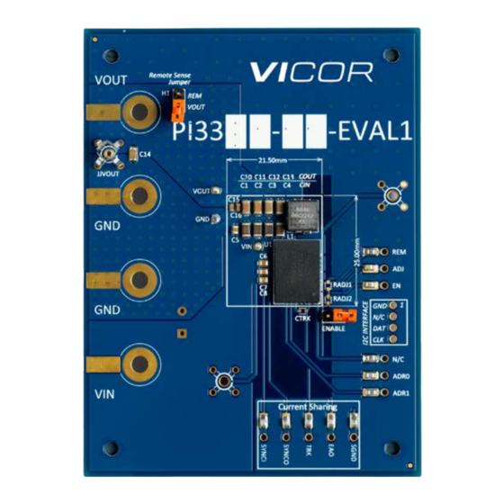
PI33xx-xx-EVAL1
ZVS Switching Regulators
2
I
C™ Digital Interface Guide
Contents
Page
Introduction
Program Capability
Fault Telemetry
I
2
C Communication
Compatibility
Interface Software Tool
20
Introduction
1
The PI33xx-xx I
2
C digital interface guide provides an overview of how to read and write to the user
accessible registers within the PI33xx-xx series. This guide details use of the Vicor I
1
software tool coupled with a USB based I
1
I
2
C communication protocol using generic tools and/or embedded hardware.
1
Program Capability
1
The PI33xx-xx devices provide an I
2
polarity (from high to low assertion) and input switching frequency synchronization phase/delay.
Margining the output is also available via the I
3
All settings are one-time programmable except for the V
volatile memory only and not retained by the device.
4
Fault Telemetry
7
Reported faults include:
n
Input Undervoltage Lockout (UVLO)
16
Input Overvoltage Lockout (OVLO)
n
16
n
Output Voltage Overvoltage (OVP)
16
n
Overtemperature Protection (OTP)
18
Slow Current Limit
n
19
Fast Current Limit
n
n
V
(internal to the SiP) Undervoltage
CC
2
I
C Communication Compatibility
The PI33xx-xx is hardware-compatible with the NXP I
(100kHz) January 2000 for all bus timing and voltage resistors levels up to 5.5V maximum. The
PI33xx-xx is configured as an I
Interface Software Tool
The Buck GUI software tool offered by Vicor allows quick access to the one time programmable
parameters and user adjustable parameters. The one time user programmable parameters include
enable (EN) polarity, synchronization (SYNCI) delay and edge trigger. User-adjustable parameters include
output margin (MRGN) level percentage and the ability to clear the fault (FLT) register. This software also
provides the user with the ability to read and decode fault telemetry information.
The Buck GUI operates under the Windows™ 7 or XP (Service Pack 3) environment. Java™ version 1.5
or greater 32-bit version is required. This software has been tested using Windows 7, 32 bit and 64 bit
and Windows XP with service pack 3.
2
C hardware interface device. Information is also provided for
2
C digital interface that enables the user to program the EN pin
2
C interface.
OUT
2
C interface.
2
C bus specification Version 2.1 Standard Mode
2
C child device with no internal bus pull up or pull down.
UG:309
2
C digital interface
margining, which settings are stored in
Page 1
Advertisement
Table of Contents

Subscribe to Our Youtube Channel
Related Manuals for VICOR PI33 EVAL1 Series

Summary of Contents for VICOR PI33 EVAL1 Series
-
Page 1: Table Of Contents
C child device with no internal bus pull up or pull down. Interface Software Tool The Buck GUI software tool offered by Vicor allows quick access to the one time programmable parameters and user adjustable parameters. The one time user programmable parameters include enable (EN) polarity, synchronization (SYNCI) delay and edge trigger. -
Page 2: Usb Interface Hardware
USB Interface Hardware The Buck GUI software is designed to work with the LinkM™ USB to I C™ interface device manufactured by ThingM. Information about the LinkM can be found at the ThingM website. A Windows‑based PC is required with a dedicated USB port. The use of USB expansion ports, especially those that are heavily loaded, is not recommended. -
Page 3: Addressing & Register Mapping
Addressing & Register Mapping Figure 2 shows the PI33xx‑xx I C™ hardware interface. The PI33xx‑xx supports floating addressing so that two address lines allows for up to eight programmable addresses. The address is 7 bit with the read/write bit not included. Table 1 shows the address range that can be achieved using all possible combinations of ADR0 and ADR1. -
Page 4: Software Installation And Operation
Table 2 Name Address HEX # Bits Description User‑accessible registers TSTMDE[2:0] Test mode register used for burning bits into non‑volatile memory MRGN[3:0] Volatile register for output voltage margining FLT[7:0] Fault Register read only FREG_CLR Register for clearing the Fault Register‑writing address clears register ENA_POL EN pin polarity programming bit SYN[3:0]... - Page 5 Figure 4 LinkM™ detection followed by Buck GUI main screen After the user observes a successful main screen like the one shown in Figure 4 and the LinkM is installed to the target board as shown in Figure 1, it is possible to use the Buck GUI to monitor and configure the PI33xx‑xx.
- Page 6 The following information is intended to provide the user with a description of the various “soft” buttons and user menus available in the Buck GUI. The “File” menu provides “Exit” as the only option available when left clicking on it. If the user chooses “Exit”, a dialog box will pop up to allow the user to confirm their selection.
-
Page 7: Fault Telemetry Command Structure
The “Clear” button allows the user to clear the PI33xx‑xx fault telemetry information. The “ENA POL” button allows the user to read the EN polarity by left clicking on it. Changing the polarity can be accomplished by entering the desired value in the dialog box and then left clicking the “BURN”... - Page 8 Figure 6 Bus capture read fault register with generic I C™ interface The sequence for sending the data in Figure 6 applies to a generic I C interface, not the Buck GUI software. There are many devices available on the market (including microcontrollers) that may be configured for this function.
- Page 9 Figure 8 C™ bus capture input undervoltage fault register read using Buck GUI and LinkM™ Figure 9 Buck GUI capture of input undervoltage fault Figure 10 shows several more common faults displayed by the Buck GUI along with the corresponding C bus capture of each event.
-
Page 10: Configuration Programming
Figure 10 Buck GUI capture of common faults with corresponding I C™ Data Figure 11 C bus capture Configuration Programming The PI33xx‑xx has three programming registers that can be changed by the user as a one‑time change only. Of each register, any bit that is not set may be set. The programming requires burning internal fuse links as permanent memory. - Page 11 To understand the relationship between the synchronization timing and the PI33xx‑xx operation, an overview of the PI33xx‑xx power train timing is shown in Figure 12. There are three main timing states in the ZVS buck topology, T1, T3 and T4 as defined below: T1: T1 defines the start of a power cycle when the clamp switch has opened and the zero voltage switching resonant action has started, followed by the turn on of Q1 and continuing until Q1 turns off.
- Page 12 Figure 13 PI33xx‑xx ZVS buck sync to T1 timing relationship Start of T1 (ZVS) Start of T1 (ZVS) where VS = Ch3 VS1 Turn on of high side Turn on of high side MOSFET MOSFET External sync pulse External sync pulse falling edge falling edge SYN[3:0]...
- Page 13 Figure 14 PI33xx‑xx SYNC = “1000” timing Figure 15 PI33xx‑xx SYNC = “1111” 1/4MP UG:309 Page 13...
- Page 14 Figure 16 PI33xx‑xx SYNC = “1110” 1/3MP Figure 17 PI33xx‑xx SYNC = “1101” 1/2MP UG:309 Page 14...
- Page 15 Figure 18 PI33xx‑xx SYNC = “1100” 2/3MP Figure 19 PI33xx‑xx SYNC = “1001” 3/4MP UG:309 Page 15...
-
Page 16: Programming Initial Conditions
Programming Initial Conditions Once the user has selected the configuration for the timing register, the burn process can be initiated. To begin this process, the user must be ready to be able to enable and disable the PI33xx‑xx, since this is required to enter the burn mode and actually burn the bits. - Page 17 When the user disables the target, another prompt will provide notification to enable the target again as shown in Figure 22. When the unit is enabled, the output voltage will remain low as if the PI33xx‑xx was still disabled. This is normal. The Buck GUI will next write “01h” into the SYN[3:0] register. Figure 22 SYNC “0001”...
-
Page 18: Enable Polarity
Configuration Example – Enable Polarity Figure 25 shows the complete procedure for changing the enable polarity along with the I C™ bus capture of all of the commands required to make the changes using Buck GUI or some other generic software. -
Page 19: Setting Kill Bit
Configuration Example – Setting Kill Bit The procedure for setting the KBIT2 register to prevent any further programming is outlined in sequence in Figure 26. The SYN[3:0] register has been programmed to “1111” and the ENA_POL register has been programmed to “1” in advance. Like the previous procedures, the first two bus transactions occur while the PI33xx‑xx is enabled and the final transaction occurs while the PI33xx‑xx is disabled. -
Page 20: Error Messages
Error Messages Missing or Malfunctioning I C™ Interface Error The error message shown in Figure 27 occurs only at the first boot of the Buck GUI each time the program is executed. During program initialization, the software determines the existence of the LinkM™... - Page 21 Burn Failed Error The error message shown in Figure 29 occurs only during a failed program attempt. Here, the value that is programmed into the associated register does not match the value that was entered into that registers dialog box prior to executing the programming operation. The most likely cause of this error is a missed enable or disable step during the programming procedure.
- Page 22 ANY AND ALL LIABILITY FOR INCLUSION AND/OR USE OF VICOR PRODUCTS IN SUCH EQUIPMENT OR APPLICATIONS AND THEREFORE SUCH INCLUSION AND/OR USE IS AT YOUR OWN RISK. Terms of Sale The purchase and sale of Vicor products is subject to the Vicor Corporation Terms and Conditions of Sale which are available at: (http://www.vicorpower.com/termsconditionswarranty) Export Control This document as well as the item(s) described herein may be subject to export control regulations.
Need help?
Do you have a question about the PI33 EVAL1 Series and is the answer not in the manual?
Questions and answers