Table of Contents
Advertisement
file:///E:/PV-9661_PV-9662/SVC/s0000000000.html
Service Manual
TOP NEXT
ORDER NO. MKE9901002C1
B3
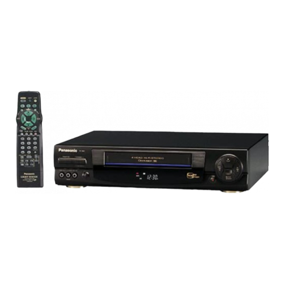
Video Cassette Recorder
PV-9661/PV-9662
●
© 1999 Matsushita-Kotobuki Electronics Industries LTD. All rights reserved. Unauthorized copying and distribution is a
violation of law.
file:///E:/PV-9661_PV-9662/SVC/s0000000000.html (1 z 2) [2006-01-28 11:08:20]
Advertisement
Table of Contents


Need help?
Do you have a question about the Omnivision PV-9661 and is the answer not in the manual?
Questions and answers