
Related Manuals for BHI NEDSP900

Summary of Contents for BHI NEDSP900
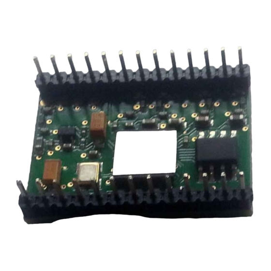
- Page 1 Ltd PO Box 318, Burgess Hill, RH15 9NR England. Tel: +44 (0)1444 870333 info@bhi-ltd.com, www.bhi-ltd.com (Picture of a basic assembled unit) Handbook for NEDSP900 Development Board Document: HB07-003-10 Issue: B...
-
Page 2: Table Of Contents
NEDSP900 Development Board Contents Introduction Recommendation Board Mechanics General Specifications The inputs SK6 Speaker/Headphone/Line Signals SK7 Microphone Input Signals 2.2.2 Electret Bias Balanced Input Pre=amplifiers Signal Input Selection Overload Indicators Gain Settings Setting the gain for SK7 (Microphone input) Noise Reduction Settings... -
Page 3: Introduction
NEDSP900 Development Board Introduction The NEDSP900 is a dual channel audio DSP Noise Suppression pcb module for improving the speech quality in Voice communication systems used in noisy environments. It is capable of handling a wide range of audio inputs and providing up to 40dB of noise suppression. The module operates on a single supply rain with on‐board voltage regulation and clock oscillator. -
Page 4: General Specifications
NEDSP900 Development Board General Specifications Operating voltage: 8 to 16v d.c. Note: While Current and Reverse Polarity protection has been built into the Power circuitry on this PCB, please check that the power lead is connected with the correct polarisation before applying power. -
Page 5: Sk6 Speaker/Headphone/Line Signals
This socket allows for stereo speakers/headphone signals to be input, matched and attenuated. The input connection Tip is connected to Channel 1 of the NEDSP900 module, while the first Ring is connected to Channel 2 of the module. Each channel has attenuation/matching facilities... - Page 6 NEDSP900 Development Board internal source, such as batteries. To make sure that you are using the correct connections always check with the manufacturers’ data sheet. The Bias is provided jumper PL19 this applies a fixed Bias to either the Ring or Tip of the jack plug. Of course if the microphone requires no bias or has an internal biasing system, then the Jumper across PL19 can be removed.
-
Page 7: Balanced Input Pre=Amplifiers
Where the single microphone (SK7) or the balanced input pre-amplifiers are being used, these indicators while monitoring, will not be effective as the signal will be much lower and you will be relying on the NEDSP900 internal gain system to increase the levels. - Page 8 When using a Line input make sure that the Jumpers are removed all together. NEDSP900 Gain Settings The NEDSP900 Gain is set using SW2 for Channel 1 and SW3 for Channel 2. Channel 1 has a gain setting capability of up to 30dB, while Channel 2 has gain settings up to 18dB only.
-
Page 9: Setting The Gain For Sk7 (Microphone Input)
NEDSP900 Development Board Channel 1 Gain 1 Gain 1 Channel 2 Gain 2 Gain 2 Input (mV P-P) (Spec. dB) (Meas. dB) Input (mV P-P) (Spec. dB) (Meas. dB) 2000 1940 12.5 12.2 15.2 15.5 17.7 17.8 20.2 23.2 25.0 27.1... -
Page 10: Outputs
Users should be aware that as these are wired for Stereo Output. Monaural jack plugs should not be used as this could cause damage to the circuitry. If a mono output is required it is recommended that stereo jack plug is used with just the required channel wired. If in doubt, consult bhi Ltd. Line Drive This is capable of driving up to 1 Volt P-P into a 600 Ohm (resistive) load and can drive as high as 2Volts p-p into higher impedances. -
Page 11: Headphone/Speaker Output
To allow for monitoring of both input and output audio signals as well as allowing for external control of the NEDSP900 module from signals ‘off the PCB’ provision has been made for additional connectors, some of them already fitted and their use is easily identifiable from the Circuit Diagrams (see Appendix Audio Monitor Points A set of audio Monitor points has been provided for the user to ‘hook’... -
Page 12: Noise Reduction Control
You will note from the previous page, that the switches are ON to get the appropriate line to activate. The NEDSP900 provides a weak pull up to its internal power rail of 1.8Volts, therefore when the switch is activated the appropriate pin is taken to ground. - Page 13 1.8K There is no logic inversion with this circuit. Circuit d) - This lets the external control logic pull the NEDSP900 logic down only and the diode becomes back biased when the external logic goes high, leaving the NEDSP900 logic to pull up itself. R6 provides a pull down function to give the Diode...
-
Page 14: Algorithm 'Hold' (Sf)
NEDSP900 Development Board effect on the weak pull up resistance of the NEDSP900. Again there is no logic inversion with this circuit. Algorithm ‘Hold’ (SF) This is a special facility (SF) that may be useful where this module is incorporated in certain intercom systems (half duplex). -
Page 15: Connector Specifications
NEDSP900 Development Board Connector specifications The board has the following connections to facilitate power, signal and control connections. The information is given here such that the user can obtain the correct connectors to interface with these or fit to the PCB... - Page 16 NEDSP900 Development Board Appendix A - PCB Documentation and BOM Board Topside Layout Board Bottom side Layout Power Input on this end...
- Page 17 NEDSP900 Development Board Schematic Diagram Sheet 1 of 5 – Output Buffer and Line Driver...
- Page 18 NEDSP900 Development Board Schematic Diagram Sheet 2 of 5 – NEDSP900 and Control Switches...
- Page 19 NEDSP900 Development Board Schematic Diagram Sheet 3 of 5 – Balanced Audio Inputs (See also Appendix B)
- Page 20 NEDSP900 Development Board Schematic Diagram Sheet 4 of 5 – Speaker and Microphone Input Interface with Overload Indicator...
- Page 21 NEDSP900 Development Board Schematic Diagram Sheet 5 of 5 – Power Input Filtering and Regulation with Headphone Amplifier...
- Page 22 NEDSP900 Development Board Bill of Materials - BOM The following is the BOM for the complete PCB (including the Balanced input Amplifiers) Item Description Part No. Supplier Variable Resistors R1, R65 ALPS RK12 10K Log Rapid Resistors Axial R66, R67 1R0/ 0.6W Metal Film...
- Page 23 NEDSP900 Development Board Item Description Part No. Supplier IC’s Through Hole DE7805 47-3313 Rapid Inductors SMT High Current L10 - L12 10uH 182-8172 Inductors SMT 0805 L1 - L3 10uH 233-3632 LED's SMD 0805 LED1, LED2 Red (Kingbright KP-2012IT) 72-8560...
- Page 24 NEDSP900 Development Board Item Description Part No. Supplier Connections PL21 - PL23 Molex KK 2 way 22-0838 Rapid PL6, PL7, PL18 Molex KK 3 way 22-0840 Rapid JP1 - JP4, JP8 2 Way Jumper Header 54-3943 Rapid PL16, PL17, PL19...
- Page 25 NEDSP900 Development Board Appendix B - Balanced Audio inputs The board has been designed with 2 off balanced input amplifiers, meant for microphones. These are available on the PCB, but require to be populated with components to enable their use. The inputs are carried out using standard Molex KK connectors.
- Page 26 These just add a 3dB roll off and have initially been calculated to give a corner frequency of around 10 kHz. Note: The NEDSP900 DSP has a roll off of around 5 kHz and the circuits that follow have also been tailored to roll off at no more than around 6 kHz.
- Page 27 NEDSP900 Development Board Biasing As the amplifiers are operating on a single supply rail they have no negative supply and therefore Ground becomes the negative supply, in which case we create a ‘false’ ground rail by taking the Non- Inverting input (IN +) of the Amplifier components, via R30, to half the rail voltage using R44 and R45.
- Page 28 NEDSP900 Development Board Bill of Material for Balanced Input amplifiers Item Description Part No. Supplier Resistors SM 0603 1% R29, R40, 470R 72-9826 Rapid R24 - R26, R35, R42, R43 72-9931 Rapid R22, R23, R33, R34, R53, R55, R57 72-9838...
- Page 29 NEDSP900 Development Board Appendix – C Fitting the board to an enclosure As previously stated this PCB is meant for development purposes only, however, it’s understood that in certain circumstances there may be a requirement to turn this stand-alone PCB into a complete unit to be part of an initial system test.
- Page 30 NEDSP900 Development Board 14.0 14.0 35.0 35.0 15.0000 35.0 HOLES: A - 5.5mm Dia. (4 Positions) B - 9.5mm Ø (2 Positions) C - 12mm Ø (1 Position) Above – End panel drilling patterns – note that the dimensions should be taken from the centre of the side of each panel.
- Page 31 NEDSP900 Development Board Preparing the PCB The indicators are surface mount and therefore little use in the enclosure, however, we have included Header positions PL21, PL22 and PL23 to allow leaded LEDs or wires to be connected to the PCB. The PCB has been designed to use standard Molex KK series headers and receptacles to ease assembly into a case.
- Page 32 NEDSP900 Development Board Front Panel of PCB fitted to Hammond manufacturing 1455L1602 case Rear Panel of PCB fitted to Hammond case...
- Page 33 NEDSP900 Development Board Addendum to PCB Model A07-001-10 (Issue:1) Due to some tracking errors, two traces have been omitted on the PCB. 1. The main omission is of the 2 audio amplifier output to the Headphone/Speaker socket. The affected PCB’s have all been modified as shown in the attached pictures below:...
- Page 34 NEDSP900 Development Board b. Using the tip of a sharp scalpel gently remove the solder resist on the ground area opposite the end of R44. d. While fitting R44 make sure that the end of the resistor is soldered to the pad and to the...
Need help?
Do you have a question about the NEDSP900 and is the answer not in the manual?
Questions and answers