
Summary of Contents for Elektor Fortissimo-100
- Page 1 Construction Manual Elektor Fortissimo-100 Power Amplifier Kit jump rter from project to product Ton Giesberts...
- Page 2 Elektor Fortissimo-100 Power Amplifier Kit Designed by Ton Giesberts - Elektor Labs Construction Manual V1.0 – date: September 8, 2022, © Elektor International Media b.v. ● 3...
- Page 3 Elektor Fortissimo-100 Power Amplifier Kit Notice: This manual is only available as a downloadable PDF at: www.elektor.com/20273. ● 4...
-
Page 4: Table Of Contents
23 – Schematics and PCB Layouts Notice This document is complementary to the information contained in: 1. the editorial article “The Elektor Fortissimo-100 Power Amplifier” published in Elektor Magazine edition 11&12 2022; 2. the engineering background and discussions posted on the Elektor Labs website. - Page 5 The circuits described in the manual are for domestic and educational use only. All drawings, photographs, PCB layouts, and article texts are copyright Elektor International Media b.v. and may not be reproduced, transmitted, or stored in any form in whole or in part without the prior written consent from the Publisher.
-
Page 6: Kit Contents
• All parts listed in the Bill of Materials (BOM) found at the end of this document (Section 19). • Construction Manual – Downloadable PDF. Figure 1. Contents of the Fortissimo-100 Power Amplifier kit as supplied by the Elektor Store. Before embarking on the construction of the Kit, be sure to inspect the contents using the Bill of Materials and the photos that follow. - Page 7 Elektor Fortissimo-100 Power Amplifier Kit Figure 2. The resistors and small capacitors in the kit. ● 8...
- Page 8 1 – Kit Contents Figure 3. The electrolytic capacitors in the kit. Figure 4. The small transistors, diodes, and other parts in the kit. ● 9...
- Page 9 Elektor Fortissimo-100 Power Amplifier Kit Figure 5. The larger transistors. Figure 6. The ceramic pads (washers) and the relay in the kit. ● 10...
- Page 10 1 – Kit Contents Figure 7. The mechanical parts in the kit. Figure 8. The SK104 heatsinks in the kit. ● 11...
-
Page 11: Introduction
Elektor Fortissimo-100 Power Amplifier Kit Figure 9. The SK53-100-SA heatsink in the kit. 2 – Introduction Notice: It is strongly advised to closely read the entire Construction Manual before starting the construction of the amplifier. The design, especially the placement of the power transistors T17–T22 and the PCB, is aimed at easy replication. -
Page 12: Tools Needed
3 – Tools Needed (amplifier PCB) connect the output of the amplifier to K6 (LS+) and K7 (LS–) on the protection PCB and from there via the relay and output terminals K8 and K9 to the loudspeaker. “Faston” connectors K8 and K9 (PCB versions) make sure the series resistance of this connection to the cable is extremely low. -
Page 13: Locating And Drilling Holes In The Heatsink, For The Pcb Standoffs
Elektor Fortissimo-100 Power Amplifier Kit 4 – Locating and Drilling Holes in the Heatsink, for the PCB Standoffs Figure 10. The bare PC boards for the amplifier and protection circuitry, as supplied in the kit. Figure 11. Amplifier PCB used as drilling template. - Page 14 4 – Locating and Drilling Holes in the Heatsink, for the PCB Standoffs The amplifier PCB is placed in the center on the heatsink, 1 mm from the edge where C1 is located, and fixed temporarily with sellotape so the six positions for the metal standoffs can be marked out (scored). Use a 3.5-mm drill bit and with some pressure turn it counterclockwise in the six holes located at the short sides of the PCB, taking great care to avoid damage to the PCB.
-
Page 15: Bending The Output Stage Transistor Leads
Elektor Fortissimo-100 Power Amplifier Kit 5 – Bending the Output Stage Transistor Leads Figure 13. Bent leads of the TO-220 and TO-264 transistors in the output stage. Bend all leads of the transistors (T17–T22) perpendicular toward the front of the transistors (Figure 13). To avoid excessive force exerted from the leads to the package of the large power transistors, use a 2-mm drill bit and a small vice. -
Page 16: Locating And Drilling Holes In The Heatsink, For The Transistors
6 – Locating and Drilling Holes in the Heatsink, for the Transistors 6 – Locating and Drilling Holes in the Heatsink, for the Transistors Figure 14. Preparations for marking the 3-mm holes required for the transistors. Before mounting any parts on the PCB, locate the position of the holes for the six screws to secure the transistors to the heatsink. - Page 17 Elektor Fortissimo-100 Power Amplifier Kit Figure 15. Marked-out positions for the six holes to be drilled (prototype). Figure 16. Six 3-mm holes drilled for the transistors in the output stage. After drilling the holes, place the transistors in position with their screws.
-
Page 18: Small Resistors And Diodes
7 – Small Resistors and Diodes Now almost all parts can be fitted on the PCBs. Start with the lowest components, small resistors and diodes (D1…D5). 7 – Small Resistors and Diodes Figure 17. The small resistors and diodes soldered onto the two boards. ●... -
Page 19: Axial Power Resistors And Ic Socket
Elektor Fortissimo-100 Power Amplifier Kit 8 – Axial Power Resistors and IC Socket Figure 18. Axial power resistors and 8-pin IC socket (pos. IC3) soldered onto the amp board. 9 – Small Capacitors and Input Terminal Pins Figure 19. The small capacitors also soldered onto the amplifier board. -
Page 20: Finishing The Assembly Of The Protection Pcb
10 – Finishing the Assembly of the Protection PCB Place and solder the small capacitors, the smallest ones first: C3, C10, C11, C32, C4, C5, C12, C2, C13, C14, C18, C19, C29, C17, C33, C28. Next, the larger/higher-value capacitors: C6, C7, C8, C9, C30, C31, C34 , input terminal pins, C1. -
Page 21: Small Transistors, Leds, Radial Power Resistors, And Large Capacitors
Elektor Fortissimo-100 Power Amplifier Kit At this point, finish fitting the rest of the components on the small PCB: T23, T26, T27, T24, T25, K5, Faston tabs K8 and K9 (including two 8-mm M3 screws/nuts/washers and finally, the inductor (13 turns of 1.5-mm diameter enameled copper wire), and relay RE1. -
Page 22: Placing The Loudspeaker-Signal Through-Contact Standoffs
12 – Placing the Loudspeaker-Signal Through-Contact Standoffs If you have enough transistors, it’s favorable to select the input tran- sistors pairs T1/T2 and T3/T4 for identical U and h values. The same applies to the transistors in the second differential amplifiers, T9/ T10 and T11/T12. -
Page 23: Transistors T13
Elektor Fortissimo-100 Power Amplifier Kit Figure 24. Each of the two 30-mm standoffs is secured with an 8-mm M3 cheese head screw. The two metal standoffs that connect the amplifier output lines of the main PCB to the smaller PCB above it can now be fitted and secured with an 8-mm long M3 cheese head screw. - Page 24 13 – Transistors T13…T16 and the Small Heatsinks Transistors T13-T14 and T15-T16 can now be mounted on the small heatsinks. A thermal relief in the leads of each transistor is recom- mended to reduce mechanical stress caused by temperature changes. It’s best to make a small bend in the leads, away from the heatsink.
- Page 25 Elektor Fortissimo-100 Power Amplifier Kit Figure 27. The two small heatsinks and transistors T13…T16 soldered in place. Before securing the transistors on the heatsinks, apply a small amount of thermal grease to the back of each transistor. No insulation is need- ed since the package of these transistors is completely plastic.
-
Page 26: The Output-Stage Transistors
14 – The Output-Stage Transistors 14 – The Output-Stage Transistors Figure 28. View of the PCB and the output stage transistors provisionally secured to the heatsink. Figure 28 shows the six output stage transistors fastened temporarily with screws and nuts to enable them to be soldered. Also, the PCB is fixed onto the 10-mm long standoffs on the heatsink with 30-mm long standoffs (or use nuts for now). - Page 27 Elektor Fortissimo-100 Power Amplifier Kit Figure 29. The output stage transistors are soldered, and thermal grease is applied to their backs. As a minimum, solder the two leads at either side of each large power transistor without melting any plastic of various capacitors. Do more leads if possible.
- Page 28 14 – The Output-Stage Transistors Figure 30. Slide the ceramic washers (pads) over the screw threads before positioning the PCB with the transistors. Place the heatsink upright with the holes for the transistors at the top. Insert the six (black) screws halfway through the heatsink. The 16- mm, black screws take T19…T22, and the 12-mm, black screws take T17 and T18.
- Page 29 Elektor Fortissimo-100 Power Amplifier Kit Figure 31. Top view of the finished amp PCB with the output stage transistors secured to the heatsink. Carefully maneuver the PCB onto the standoffs on the heatsink, mak- ing sure the screws pass through the transistor holes while the ceramic washers remain in position.
-
Page 30: Final Assembly
+40 V power supply between the two PCBs (K2 to K5) is missing. The photos show the construction of the first com- pleted prototype for measurements conducted at Elektor Labs. At this stage LED5 wasn’t fitted on the protection PCB. - Page 31 Elektor Fortissimo-100 Power Amplifier Kit Figure 33. Left-side view of the Fortissimo-100 Power Amplifier. ● 32...
- Page 32 15 – Final Assembly Figure 34. Right-side view of the Fortissimo-100 amplifier. ● 33...
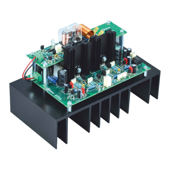
- Page 33 Elektor Fortissimo-100 Power Amplifier Kit Figure 35. Broadside view of the Fortissimo-100’s output stage. Figures 33, 34, and 35 show the assembly and initial wiring of the first prototype for measurements. Figure 36. The finished Fortissimo-100 Audio Power Amplifier that was used for testing.
-
Page 34: Recommendations For The Enclosure
MKDSN 1,5/ 3-5,08 supplied in the kit is 1.5 mm However, the size of the pads at the top side of K1 permit soldering much thicker wire directly onto the PCB. In the Elektor prototype ver- sion, the output of the SMPS has three “Faston” (a.k.a. spade) termi- nals, hence thicker wire is not a problem here. -
Page 35: Selecting Bc546B/Bc556B Transistors For Differential Pairs
Elektor Fortissimo-100 Power Amplifier Kit even cause instabilities and oscillations due to the high speed of the amplifier as its gain-bandwidth product is 2.8 GHz! Star-Ground of the amplifier is in the center of the PCB, located at the loudspeaker Ground connection, K4. -
Page 36: The Smps800Re Power Supply
NPN pair and the PNP pair, and the next best combination goes in the second stages. 18 – The SMPS800RE Power Supply Figure 38. The Fortissimo-100 amplifier experimentally connected to the SMPS800RE power supply. ● 37... - Page 37 The following plot shows an FFT of 1 kHz at 1 W in an 8-ohm load us- ing the SMPS800RE as a power supply for the Fortissimo-100 amplifier built with parts from a kit. The spectrum is essentially clean, right up 130 kHz.
-
Page 38: Bill Of Materials
19 – Bill of Materials The Levels of the 2 and 3 harmonic are –112.6 dB and –118.5 dB down, respectively. THD amounts to a trifling 0.00026%. 19 – Bill of Materials (PCB 210634-1 v1.1, schematic v1.2) Resistor (small 0.6 W resistors are metal film) R1,R74 = 1 MΩ, 1%, 0.6 W R2,R4 = 390 Ω, 1%, 0.6 W R3,R5,R20,R23,R64,R66,R69 = 10 kΩ, 1%, 0.6 W... - Page 39 Elektor Fortissimo-100 Power Amplifier Kit R62 = 1.2 kΩ, 1%, 0.6 W R63 = 270 Ω, 1%, 0.6 W R65,R70,R71 = 10 MΩ, 1%, 0.6 W R68 = 0 Ω, jumper wire R72 = 3.3 MΩ, 1%, 0.6 W R73 = 100 kΩ, 1%, 0.6 W R75 = 150 kΩ, 1%, 0.6 W...
- Page 40 19 – Bill of Materials C32 = 10 nF, 10%, 50 VDC, pitch 5 mm, X7R, body size 2.5 x 7.2 mm max. C33 = 1 µF, 5%, 63 VDC, pitch 5/7.5 mm, PET, body size 7.6 x 9.7 mm max. C34 = 22 µF, 20%, 35 VDC, bi-polar, D 8 mm max., pitch 2.5/3.5 mm Inductor...
- Page 41 Elektor Fortissimo-100 Power Amplifier Kit K3,K4 (=K6,K7) + 4 for 2nd PCB = metal standoff, 30 mm, M3, male-female (so 6 in total) K8,K9 = Faston PCB, hole 3.3 mm, tab 6.35mm x 0.81mm (42822-2 Amp/TE Connectivity or similar) RE1 = Relay 16 A /250 VAC/30 VDC, G2R-1-E 48DC Omron...
-
Page 42: Specifications
20 – Specifications 20 – Specifications Power source used: laboratory power supply rated 2 x 40 V DC, regu- lated + 2 x 10000 µF/50 V close to K1. Input sensitivity 1.076 V (94 W/8 Ω, THD = 0.1%, B = 22 kHz) Input impedance 10 kΩ... -
Page 43: Dc Voltages
Elektor Fortissimo-100 Power Amplifier Kit Intermodulation Distortion (50 Hz : 7 kHz = 4 : 1) 0.0012% (1 W, 8 Ω) 0.0015% (50 W, 8 Ω) 0.0024% (1 W, 4 Ω) 0.0041% (100 W, 4 Ω) Dynamic IM Distortion 0.0016% (1 W, 8 Ω) (3.15 kHz square wave + 0.001% (50 W, 8 Ω) -
Page 44: Web Links
LEDs (average) = 1.675 V 22 – Web Links Fortissimo-100 Power Amplifier project page on the Elektor Labs website: www.elektormagazine.com/labs/fortissimo-100 Fortissimo-100 Power Amplifier Kit on the Elektor Store website: www.elektor.com/20273 Fortissimo-100 Power Amplifier article published in Elektor Magazine: www.elektormagazine.com/magazine/NUMBER QR code... -
Page 45: Schematics And Pcb Layouts
Elektor Fortissimo-100 Power Amplifier Kit 23 – Schematics and PCB Layouts Figure 41. Schematic of the amplifier (210364-1 v1.2). ● 46... - Page 46 23 – Schematics and PCB Layouts Figure 42. Schematic of the protection circuitry (210364-1 v1.2). Figure 43. Top overlays of both PCBs (210364-1 v1.1). ● 47...
- Page 47 Elektor Fortissimo-100 Power Amplifier Kit Figure 44. Bottom views of both PCBs (210364-1 v1.1) Figure 45. Top-side copper layout for both PCBs (210364-1 v1.1). ● 48...
- Page 48 23 – Schematics and PCB Layouts Figure 46. Bottom-side copper layout for both PCBs (210364-1 v1.1). ● 49...
Need help?
Do you have a question about the Fortissimo-100 and is the answer not in the manual?
Questions and answers