
Related Manuals for Forlinx SoM FETMX8MPQ-C

Summary of Contents for Forlinx SoM FETMX8MPQ-C
- Page 1 SoM FETMX8MPQ-C/ SBC OKMX8MPQ-C ARM Cortex-A53+ Cortex-M7 Embedded Development Platform Hardware Manual Rev. 2.0 www.forlix.net Forlinx Embedded Technology Co. Ltd.
-
Page 2: Attentions
Please do not modify the product by yourself or use fittings unauthorized by us. Otherwise, the damage caused by that will be on your part and not included in guarantee terms. Any questions please feel free to contact Forlinx Technical Service Department.. - Page 3 Copyright Announcement Please note that reproduction of this User Manual in whole or in part, without express written permission from Forlinx, is not permitted.
- Page 4 Updating Record Version Date Updated Manual Carrier board Oct., 2021 V2.0 V1.0 V2.0 Carrier board PCB version updated to V2.0 1. PHY chip changed from AR8031-AL18 to YT8521; 2. Power circuited controlled by MOS, added with RC to avoid previous power drops during powering, including VSYS_5V, LVDS and audio power circuit on carrier board.
- Page 5 2.2 How to implant OS; 2.3 Software and hardware problems occured in self-modifying and programming Note: the above three points are out of Forlinx technical service range, but Forlinx will try best but can not promise to help users to solve the problems.
-
Page 6: Table Of Contents
Contents Attentions ..............................2 Chapter 1 Overview of NXP i.MX8MP SoC ......................8 Chapter 2 Introduction of SoM FETMX8MPQ-C ....................10 2.1 Exterior of SoM FETMX8MPQ-C ...................... 10 2.2 Dimension Drawing ..........................10 2.3 SoM Parameters ........................... 11 2.3.1 Frequency ..........................11 2.3.2 Power Supply .......................... - Page 7 3.4.4 Debug ............................36 3.4.5 General UART ..........................37 3.4.6 CAN ............................38 3.4.7 RS485 ............................39 3.4.8 SPI .............................. 39 3.4.9 JTAG ............................40 3.5.10 TF card ............................. 40 3.4.11 MIPI-CSI ........................... 41 3.4.12 MIPI-DSI ...........................42 3.4.13 LVDS ............................42 3.4.14 HDMI ............................43 3.4.15 Audio ............................
-
Page 8: Chapter 1 Overview Of Nxp I.mx8Mp Soc
Chapter 1 Overview of NXP i.MX8MP SoC The i.MX 8M Plus family is a set of NXP products focused on machine learning applications, combining state-of-art multimedia features with high-performance processing optimized for low-power consumption. The i.MX 8M Plus Applications Processor relies on a powerful fully coherent core complex based on a quad Cortex-A53 cluster, a Cortex-M7 coprocessor, audio digital signal processor, machine learning and graphics accelerators. - Page 9 Forlinx FETMX8MPX-C SoM can support below CPU models, the standard one we use is MIMX8ML8CVNKZAB A53 Core A53 speed Part number Temp width Device description Part difference description number i.MX 8M PlusQuad NPU, ISP, VPU,HiFi 4, CAN-FD MIMX8ML8CVNKZAB 1.6 GHz...
-
Page 10: Chapter 2 Introduction Of Som Fetmx8Mpq-C
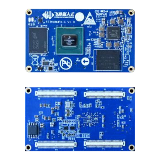
Chapter 2 Introduction of SoM FETMX8MPQ-C 2.1 Exterior of SoM FETMX8MPQ-C FETMX8MPQ-C Note: FETMX8MPX-C is available for multiple processors, so it’s printed as FETMX8MPX-C . 2.2 Dimension Drawing... -
Page 11: Som Parameters
AXK6F80337YG, carrier board connector AXK5F80537YG, the SoM is designed with four mounting holes with diameter of 2.2mm on the four corners. Users can take Forlinx carrier board designing for reference, using M2, L=2mm mounting nuts as below Length ‘L’±0.1 Thread... -
Page 12: Som Interface Speed
.3.4 SoM Interface Speed Spec. Item Note Minimum Classic Maximum Unit UART — 115200 — Mbps — Kbps — CAN FD Mbps — — SD/MMC/SDIO Mbps — — Gbps — PCIe Gbps — — 2.4 SoM Resource Peripheral Spec. CPU integrated with 2 USB3.0/ 2.0 controllers both with PHY, can support Super-speed (5Gbit/s), high-speed(480Mbit/s), full-speed(12Mbit/s), low-speed(1.5Mbit/s) Device mode: SS/HS/FS... -
Page 13: Som Fetmx8Mpq-C Pin Definition
Available for IIS, AC97, TDM and Codec/ DSP SPDIF ≤1 S/ PDIF ≤4 16-bit upcounter; JTAG 2x 5, pitch of 2.0mm headers QSPI ≤1 Used by SoM, connected to 16MB Nor Flash 2.5 SoM FETMX8MPQ-C Pin Definition 2.5.1 SoM Connector Schematic... -
Page 15: Som Fetmx8Mpq-C Pin Details
2.5.2 SoM FETMX8MPQ-C Pin Details Table 1 LEFT_UP (P1 ) connector pins (odd) Ball Signal GPIO Spec. Default LU_1 — — — LU_3 UART2_TXD GPIO5_IO25 3.3V UART2(A53 debug) data sending UART2_TXD LU_5 UART2_RXD GPIO5_IO24 3.3V UART2(A53 debug) data receiving UART2_RXD... - Page 16 LU_39 AJ8 SAI1_RXD3 GPIO4_IO5 1.8V SAI1 receivedata 3 ENET1_MDIO LU_41 AD12 SAI1_TXD3 GPIO4_IO15 1.8V SAI1 send data 3 ENET1_TD3 LU_43 AH11 SAI1_TXD2 GPIO4_IO14 1.8V SAI1 send data 2 ENET1_TD2 LU_45 AJ10 SAI1_TXD1 GPIO4_IO13 1.8V SAI1 send data 1 ENET1_TD1 LU_47 AJ11 SAI1_TXD0 GPIO4_IO12 1.8V...
- Page 17 SAI3 main clock LU_52 AJ20 SAI3_MCLK GPIO5_IO2 3.3V SAI3_MCLK LU_54 — — — SAI3 send bit clock LU_56 AH19 SAI3_TXC GPIO5_IO0 3.3V SAI3_TXC SAI3 send frame sync LU_58 AC16 SAI3_TXFS GPIO4_IO31 3.3V SAI3_TXFS SAI3 send data LU_60 AH18 SAI3_TXD GPIO5_IO1 3.3V SAI3_TXD SAI3 receive data...
- Page 18 JTAG mode select RU_65 JTAG_MOD — 3.3V JTAG_MOD RU_67 — — — CPU reset RU_69 POR_B — 1.8V POR_B PMIC power supply request RU_71 PMIC_ON_REQ — 1.8V PMIC_ON_REQ power on/ off signal RU_73 ONOFF — 1.8V ONOFF NAND_DQS NAND_DQS clock RU_75 NAND_DQS GPIO3_IO14...
- Page 19 DSI data 3+ RU_78 DSI_DP3 — — DSI_DP3 RU_80 — — — Table 5 LEFT_DOWN (P3 ) (odd) Signal Spec. Default function Ball GPIO LD_1 — — — HDMI hot plug detect LD_3 AE22 HDMI_HPD GPIO3_IO29 3.3V HDMI_HPD HDMI_DDC data LD_5 AF22 HDMI_DDC_SDA...
- Page 20 Table 6 LEFT_DOWN (P3) (even) Spec. Default function Signal GPIO Ball LD_2 — — — SPDIF clock ENET_nRST LD_4 AC18 SPDIF_EXT_CL GPIO5_IO5 3.3V SPDIF receive LD_6 AD18 SPDIF_RX GPIO5_IO4 3.3V ENET1_nRST SPDIF send ENET_nINT LD_8 AE18 SPDIF_TX GPIO5_IO3 3.3V LD_10 —...
- Page 21 Table 7 RIGHT_DOWN (P4) (odd) Spec. Default function Signal GPIO Ball RD_1 — — — CSI1 clock+ RD_3 CSI1_CKP — — CSI1_CKP CSI1 clock- RD_5 CSI1_CKN — — CSI1_CKN RD_7 — — — CSI1 data 0- RD_9 CSI1_DN0 — — CSI1_DN0 CSI1 data 0+ RD_11...
- Page 22 Table 8 RIGHT_DOWN (P4 ) (even) Spec. Default function Signal GPIO Ball RD_2 — — — LVDS1 data 3+ RD_4 LVDS1_TX3_P — — LVDS1_TX3_ LVDS1 data 3- RD_6 LVDS1_TX3_N — — LVDS1_TX3_ RD_8 — — — LVDS1 clock+ RD_10 LVDS1_CLK_P —...
-
Page 23: Som Fetmx8Mm-C Pin Spec
2.6 SoM FETMX8MM-C Pin Spec. 2.6.1 Power Pins Signal I/ O Default function Pin NO. RD_73 RD_75 RD_77 VSYS_5V Power input Som power supplying pin, 5V RD_79 RD_76 RD_78 RD_80 Carrier board SD card power supply, RD_66 VSD_3V3 Power output Power 3.3V RD_68... -
Page 24: Usb
2.6.5 USB Peripheral Signal Default function Pin No. USB1_VBUS_3V3 USB1_VBUS detect RU_9 USB1_DP USB1 data+ RU_3 USB1_DN USB1 data- RU_5 USB1_RXN USB1 receive- RU_4 USB1_RXP USB1 receive+ RU_6 USB1 USB1_TXN USB1 send- RU_10 USB1_TXP USB1 send+ RU_12 USB2_VBUS_3V3 USB2_VBUS detect RU_11 USB2_RXN USB2 receive-... -
Page 25: Uart
SAI1_RXD5 SAI1 receive data 5 LU_65 SAI1_RXD6 SAI1 receive data 6 LU_67 SAI1_RXD7 SAI1 receive data 7 LU_69 SAI1_TXD6 SAI1 send data 6 LU_73 SAI1_TXD7 SAI1 send data 7 LU_75 SAI1_MCLK SAI1 main clock LU_77 SAI2_RXC SAI2 receive bit clock LU_32 SAI2_TXC SAI2 send bit clock... -
Page 26: Jtag
2.6.10 JTAG Peripheral Signal Default function Pin No. JTAG_TMS JTAG test mode select RU_57 JTAG_TDO JTAG test data serial output RU_59 JTAG_TDI JTAG test data serial input RU_61 JTAG_TCK JTAG detect clock RU_63 JTAG JTAG_MOD JTAG mode select RU_65 2.6.11 Ethernet Peripheral Signal Default function... -
Page 27: Mipi Csi
2.6.12 MIPI CSI Peripheral Signal Default function Pin No. CSI1_CKP CSI1 clock+ RD_3 CSI1_CKN CSI1 clock- RD_5 CSI1_DN0 CSI1 data 0- RD_9 CSI1_DP0 CSI1 data 0+ RD_11 CSI1_DN1 CSI1 data 1- RD_15 MIPI_CSI_P1 CSI1_DP1 CSI1 data 1+ RD_17 CSI1_DN2 CSI1 data 2- RD_21 CSI1_DP2 CSI1 data 2+... -
Page 28: Lvds
2.6.14 LVDS Peripheral Signal Default function Pin No. LVDS1_TX3_P LVDS1 data3+ RD_4 LVDS1_TX3_N LVDS1 data3- RD_6 LVDS1_CLK_P LVDS1 clock+ RD_10 LVDS1_CLK_N LVDS1 clock- RD_12 LVDS1_TX2_P LVDS1 data2+ RD_16 LVDS1_TX2_N LVDS1 data2- RD_18 LVDS1_TX1_P LVDS1 data1+ RD_22 LVDS1_TX1_N LVDS1 data1- RD_24 LVDS1 LVDS1_TX0_P LVDS1 data0+... -
Page 29: Sd Card Slot
2.6.17 SD card slot Peripheral Signal Default function Pin No. SD1_DATA4 SD1 data bit 4 LD_52 SD1_DATA5 SD1 data bit 5 LD_54 SD1_DATA6 SD1 data bit 6 LD_56 SD1_DATA7 SD1 data bit 7 LD_58 SD1_STROBE SD1 strobe signal LD_62 SD1_RESET_B SD1 reset signal LD_64 SD1_DATA2... - Page 30 The minimum system schematic please refer to Appendix4, except minimum system, we kindly suggest users to mount some peripherals such as debug port to check serial output information, preserve OTG for firmware installation, and then refer to Forlinx SoM default definition to expand needed functions.
-
Page 31: Chapter 3 Okmx8Mpq-C Carrier Board Features
Chapter 3 OKMX8MPQ-C Carrier Board Features 3.1 Overview of OKMX8MPQ-C OKMX8MPQ-C single board computer consists of carrier board and SoM, the SoM can connect with carrier board by three ultra thin connectors. 3.2 OKMX8MPQ –C Dimensions... -
Page 32: Carrier Board Features
SoM. Standard of the selected heat sink by Forlinx is 38mm* 38mm* 23mm, picture is as below 3.3 Carrier Board Features Peripheral QTY Spec. -
Page 33: Okmx8Mpq-C Carrier Board Introduction
Note: When users make carrier board designing, please refer to Forlinx carrier board power sequence that SoM outputs VDD_3V3 to enable carrier board DC-DC power, so that SoM can be powered firstly... -
Page 35: Key
3.4.2 Key SYS_nRST is a reset key. ONOFF is a power key, press it in ON mode, it will trigger a interrupt, and long press this key to power off it forced. Press this key in OFF mode, the internal power management status will switch to ON mode. -
Page 36: Debug
SD: the development board takes TF card for system guiding, thus to install firmware for the board by TF card QSPI: system firmware boot from QSPI NorFlash. Note: The pulled-up voltage of BOOT signal is from VDD_3VS output from SoM. 3.4.4 Debug There are 2 debug ports from SoM, UART2 is for A53 debug and UART4 is for M7 debug. -
Page 37: General Uart
3.4.5 General UART There are 4 general serial ports on carrier board, rate up to 12Mbps, designed as 2*5pin-2.0mm simple horn seat . -
Page 38: Can
3.4.6 CAN Two CAN ports are available on carrier board, comply with CAN-FD, designed with 1500VDC electrical isolation and ESD4 solution. The headers are from P29, and we kindly suggest users to take it common-grounded when using it for communication. -
Page 39: Rs485
3.4.7 RS485 One RS485 from P29 is available on carrier board, designed with 1500VDC electrical isolation and ESD4 solution. MAX13487 can control transceiving direction automatically. P28 is short circuit jumper for 120 Ω resistor of AB wire. and we kindly suggest users to take it common-grounded when using it for communication. -
Page 40: Jtag
3.4.9 JTAG P38 on carrier board with pitch of 1.27mm is a JTAG port, it could be suspended if not it’s not needed. BOOT_MODE[0:3], JTAG_MOD and POR_B should be up pulled to 111111 to get into i.MX8M Plus Boundary Scan mode 3.5.10 TF card SD2 of CPU is for TF card, can support HS-I TF card, rate up to 104MB/s. -
Page 41: Mipi-Csi
3.4.11 MIPI-CSI The SoM has two MIPI-CSI interfaces, CSI 1 by P31 for daA3840-30mc-IMX8MP-EVK module, and CSI2 by a FPC(P30) connector for 2 lane MIPI-CSI, can be mounted with OV5645 camera module up to 2592x1944@15fps. All CSI2 signals are available for P19 which is convenient for users to debug other camera modules. Note : 1. -
Page 42: Mipi-Dsi
Note: data should be equal with clock, differential impedance 100 Ω 3.4.13 LVDS There are two 8-lane LVDS ports on carrier board by headers with pitch of 2.0mm, it can fit Forlinx 10.1’’ LVDS module well, can support display brightness adjusting and capacitive touching. -
Page 43: Hdmi
3.4.14 HDMI One HDMI from P16 is available on carrier board, can support HDMI2.0a up to 4Kp30 and HDMI2.1 eARC, HDMI circuit contains level transfer circuit, users can take Forlinx circuit for reference Note : 1. data should be equal with clock, differential impedance 100 Ω... - Page 44 3.4.16 4G/ 5G 4G and 5G are optional and alternative. Users can choose a mini PCIe standard 4G wireless module, the default one we use is Quectel EC20, and M.2 Key B standard 5G wireless module, the one we use is Quectel RM500Q. 4G and 5G share one DCDC power and one SIM card slot and also one USB2.0 channel, mount a module to board and set DIP to correct mode, then power on the board.
-
Page 45: Wifi& Bt
3.4.17 WIFI& BT OKMX8MPQ-C is designed with an optional WIFI& BT module AW-CM358SM on carrier board, WLAN: IEEE 802.11 a/b/g/n/ac dual band WiFi up to 433.3Mbps, BT5.0 up to 3Mbps. Please use a 2.4& 5Ghz duan band antenna to enhance signal. Note: 1. -
Page 46: Pcie
3.4.18 PCIe One PCIe x1 slot with latch is available on OKMX8MPQ-C carrier board complies with PCI Express Gen3, PCIE_REF_CLK_P/N of SoM can only support input clock, it needs carrier board clock chip U42 with RC and EP with same source dual direction . Note: PCIe TX/RX data and CLK reference clock both should be processed with 85Ω... -
Page 47: Usb Host
3.4.19 USB Host It expand four USB3.0 to carrier board by USB3.0 HUB CYUSB3304, two of them are USB Type-A connectors with power anti short circuit protection, 1A limited, over-current protection controlled by USB HUB, if users don’t use a HUB chip, please design short circuit protection circuit to carrier board. -
Page 48: Usb3.0 Type-C
3.4.20 USB3.0 Type-C... - Page 49 There is one USB3.0 Type-C port on carrier board available for DFP, UFP and DRP for firmware installation. To get Type-C, the carrier board is designed with CC chip and USB Switch. Users can take Forlinx designing for reference. If users need USB2.0 OTG, the port can be simplified as below Note: 1.
-
Page 50: Ethernet
3.4.21 Ethernet Two Gigabit Ethernet port (P20) are available on OKMX8MPQ-C carrier board and 10/100/1000Mbps auto-adaptive, the upper one can support TSN. SoM RGMII is mounted with PHY chip YT8521S , and the dual-layer RJ45 connector has internal network transformer and its structure is as below. - Page 51 Simulated differential line should be with 100Ω differential impedance, interclass equal length should be≤1000mil The PCB should be designed with 4 layers at least and the circuit should be with complete reference layer, otherwise it may cause network failure; It’s kindly suggested to take Forlinx designing for reference.
-
Page 52: Led
3.4.22 LED 2 LED indicators are available on carrier board controlled by GPIO and available for users’ definition. 3.4.23 RTC The carrier board mounted with RTC by IIC3 and be compatible with cell battery by VCC_3V3 from D5, when carrier board power is cut off, the battery can supply power to RTC chip. The circuit can be compatible with RS8010SJ and PCF8563T/5. -
Page 53: Appendix 1 Carrier Board Designing Tips
6.Signals not used by SoM could be suspended, but please circuit all of them to GND. 7.power sequence We kindly suggest users taking Forlinx carrier board designing for reference, take VDD_3V3 output from SoM to enable carrier board power, strictly control power sequence, otherwise, it may cause below problems Power on current over large;... -
Page 54: Appendix 2 Connector
Appendix 2 Connector connector model on SoM is AXK6F80337YG... - Page 55 The connector matched on carrier board is AXK5F80537YG...
-
Page 56: Appendix 3 Power Consumption Sheet
Appendix 3 Power Consumption Sheet OS Linux Hardware Test Voltage in Current output Instant Peak(mA) Stable(mA) OKMX8MPQ-C mounted with OKMX8MPQ-C PCIe hard disk, 5G, 10.1’’ LVDS 1.07 0.89 display with video playing Powered with empty loaded 0.72 0.42 FETMX8MPQ-C CPU 100% loaded 0.57 Sleeping mode 0.105... -
Page 57: Appendix 4 Minimum System Schematic
Appendix 4 Minimum System Schematic Below pictures are just for reference. To make sure the SoM can work, except for VSYS_5V, it also needs SyS_nRST, BOOT configuring circuit, OTG or SD card, which will be convenient for users for firmware installation and system boot;...
Need help?
Do you have a question about the SoM FETMX8MPQ-C and is the answer not in the manual?
Questions and answers