
Related Manuals for Panasonic KX-T7453


Summary of Contents for Panasonic KX-T7453
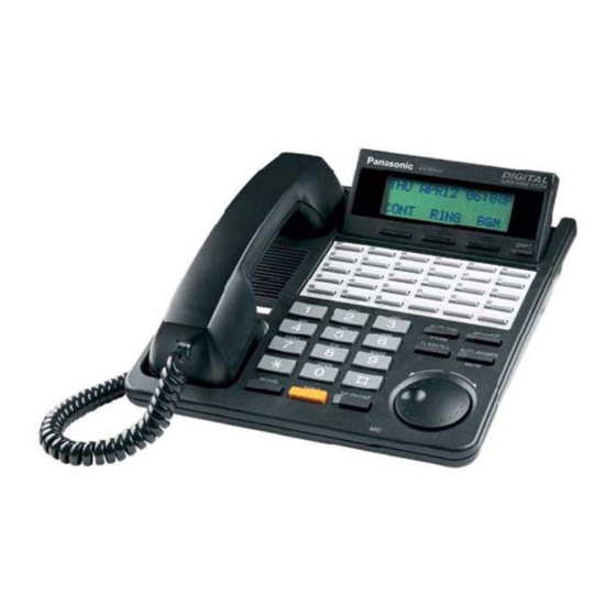
- Page 1 ORDER NO. KMS0104563C1 DIGITAL PROPRIETARY TELEPHONE KX-T7453 / KX-T7453B White Version Black Version (for U.S.A.) SPECIFICATIONS...
-
Page 2: For Service Technicians
1. CAUTION Note: When you note the serial number, write down all of the 11 digitals. The serial number may be found on the label affixed to the bottom of the unit. 2. FOR SERVICE TECHNICIANS 1. Note the following items when exchanging the LEDs (Ref. No. D100- 130, D201, D202) of Dial P.C. - Page 3 4. DISASSEMBLY INSTRUCTIONS 4.1. HOW TO REMOVE THE LOWER CABINET (Procedure 1) (1) Remove the 4 screws A. (2) Remove the lower cabinet.
- Page 4 4.2. HOW TO REMOVE THE HOOK BUTTON (Procedure 1 (1) Remove the hook button. 4.3. HOW TO REMOVE THE SWITCH AND MAIN BOARDS (Procedure 1...
- Page 5 (1) Remove the screws A. (2) Pull out the switch board connector. (3) Remove the switch board. (4) Pull out the flat cable. (See Fig. 1) (5) Remove the 2 screws B. (6) Pull out the speaker and microphone connectors. (7) Remove the main board.
- Page 6 (1) Pull out the flat cable. (See Fig. 1) (2) Remove the LCD block. (See Fig. 2) (3) Remove the 2 screws A. (4) Remove the lower cabinet. (5) Remove the LCD board.
- Page 7 5. IC DATA 5.1. IC1...
- Page 8 Name Dir. Pull Up Type Act. Block Descriptions bidir 8.0mA high PT5B03 Data Bus [3] bidir 8.0mA high PT5B03 Data Bus [2] bidir 8.0mA high PT5B03 Data Bus [1] bidir 8.0mA high PT5B03 Data Bus [0] ADR1 input 12-38k high PT5D01U Address Bus [1] ADR0...
- Page 9 output CMOS 4.0mA PC5O02 0.01 LED Row Drive [7] NROW7 output CMOS 4.0mA PC5O02 0.01 LED Row Drive [8] NROW8 output CMOS 4.0mA PC5O02 0.01 LED Row Drive [9] NROW9 input 12-38k CMOS high PC5D01U 0.01 Input Port [0] input 12-38k CMOS high PC5D01U 0.01 Input Port [1]...
- Page 11 Name Classification Function APMP Analog Analog Non-inverting input terminal of microphone amplifier M1. input Connect to the microphone. Power. Reference voltage teminal of DAC. VREFDA supply, etc. Connect the capacitor of 40 F between this terminal and pi (AG2). Ground terminal of the analog circuit. Analog Analog Output terminal for the handset receiver.
- Page 12 Input terminal for PCM data. input output Output terminal for PCM data -FSYNC Input terminal of Sync. signal for PCM interface. The frequenc of input sync. input interface signal is 8 kHz. BCLK Input terminal of shift clock pulse for PCM deta. Input pulse frequency range is 64 kHz~2.048 kHz.
-
Page 13: Key Input Control Circuit
Power Ground terminal of analog circuit. A5V4 supply, etc. 5V power terminal of analog circuit. AP2HO Analog Output terminal of microphone amplofier H2. output Connect the capacitor of 0.1 F to this terminal to cut the DC AP2HI Analog Inverting input terminal of microphone amplofier H2. Analog input Connect the capacitor of 0.1... -
Page 14: Lcd Control Circuit
7.2. LCD CONTROL CIRCUIT 1) Circuit Operation The LCD data is output from pins 32 to 35, 40 to 47 and 11 of IC6. LCD contrast adjustment is performed by the circuit composed of Q28, Q29, R109, R108 and R106. The contrast is determined only by the voltage level between V5 and VEE of IC202 and IC201. -
Page 16: Led Circuit
7.3. LED CIRCUIT 1) Circuit Operation The LED executes dynamic lighting for the status indicators, and control is executed by the output ports C0 to C5 (column) and R0 to R9 of IC1. A fixed pulse (T=1.82 msec) is output continuously from the/SCK1 terminal of IC9. This pulse is counted and the output of IC1 is shifted sequentially from C0 to C5. -
Page 17: Data Communication Circuit
7.4. DATA COMMUNICATION CIRCUIT 1) Function The data communication circuit serves the following functions: Information exchanger between the DSHS and DSHS proprietary telephone, key input information as well as data for the LED control, LCD control, etc. This information is continuously exchanged at all... - Page 18 times. 2) Circuit Operation When the DSHS propritary telephone receives an IRQ signal from the DSHS and after sending the key input information to the DSHS and receivung data for the LED control, etc., the DSHS proprietary telephone will return to the DSHS an acknowledge signal. 3) Reception The data from the DSHS is received via the H and L lines along the path shown below.
- Page 19 Layer 1 is the transmission method of Ping-Pong type which is AMI encoded. “SYNC/MAM/C/D/B1/B2/ P” data is received in the first half at 125us/frame. After 1 bit time has passed since receiving P data, “SYNC/MAM/C/D/B1/B2/P” is transmitted. 1 bit time is 512kHz. 7-bit time idle term comes after receiving P data.
-
Page 20: Reset Circuit
7.5. RESET CIRCUIT 1) Circuit Operation This circuit is used for transmission of a reset pulse to the CPU (IC6) at the following times, connecting the telephone line jack and circuit operation. The timing chart is shown below. - Page 21 The reset signal is negledted.
-
Page 22: Tone Generation Circuit
7.6. TONE GENERATION CIRCUIT 1) Function Calling tones, Busy tone, DTMF signal and Key in tone are generated in IC2. - Page 23 7.7. JOG DIAL CIRCUIT 1) Circuit Operation This unit is equipped with the JOG switch, which makes the settings of the volume, function selection speed dial, etc. easy and convenient. This JOG switch consists of 2-phase rotary encoder, and the gate array of IC1 counts the number of the rotation to control.
-
Page 24: Handset Circuit
7.8. HOOK SWITCH CIRCUIT 1) Circuit Operation The hook switch of this unit employs the photo switch consisting of LED and photo transistor. The 2kHz pulse from the gate array of IC2 causes the LED to emit the light. The light is interrupted at ON- HOOK and passes through at OFF-HOOK by the hooking bar,so that the hooking is performed controlling the light of the photo transistor. -
Page 25: Troubleshooting Guide
The voice serial data transmitted from PBX is sent to IC1 or IC2 by the serial data. The network control, gain control , A/D conversion is performed in IC2, then the data is output from the handset speaker. Q31 of the handset speaker performs the mute operation by controlling IC6. 3) Circuit diagram for transmission/reception signal path Refer to page SCHEMATIC DIAGRAM... - Page 26 8.2. THE LCD DOES NOT OPERATE.
-
Page 27: The Electronic Volume Of The Speaker-Phone Does Not Work
8.3. THE ELECTRONIC VOLUME OF THE SPEAKER-PHONE DOES NOT WORK. 8.4. THE ELECTRONIC VOLUME OF THE HANDSET DOES NOT WORK. -
Page 28: Speaker-Phone Trouble
8.5. SPEAKER-PHONE TROUBLE. 8.6. TONE DIAL TROUBLE. 8.7. HANDSET TROUBLE. -
Page 29: Terminal Guide Of Ics, Transistors And Diodes
9. TERMINAL GUIDE OF ICS, TRANSISTORS AND DIODES... -
Page 30: How To Replace The Flat Package Ic
10. HOW TO REPLACE THE FLAT PACKAGE IC If you do not have the special tools (for example: SPOT HEATER) to remove the SPOT HEATER’S Flat IC, If you have solder (large amount) a soldering iron and a cutter knife, you can easily remove IC’s even though large than 100 pin. -
Page 31: Flat Package Ic Installation Procedure
Note: If you do not fill with solder and directly cut the IC lead with the cutter, stress may build up directly in the P.C.board’s pattern. If you do not fill with large quantities of solder as in step 1 the P.C.board pattern may be removed. -
Page 32: Bridge Modification Procedure
1. Temporary fix FLAT PACKAGE IC by soldering on two marked pins. *Check the accuracy of the IC setting with the corresponding soldering foil. 2. Apply flux for all pins of FLAT PACKAGE IC. 3. Solder using the specified solder, in the direction of the arrow, by sliding the soldering iron. -
Page 33: Accessories And Packing Materials
13. ACCESSORIES AND PACKING MATERIALS... -
Page 34: Replacement Parts List
14. REPLACEMENT PARTS LIST Note: 1. The marking (RTL) indicates that the Retention Time is limited for this item. -
Page 35: Cabinet And Electrical Parts
After the discontinuation of this assembly in production, the item will continue to be available for a specific period of time. The retention period of availability depends on the type of assembly and the laws governing parts and product retention. After the end of this period, the assembly will no longer be available. - Page 36 Ref. No. Part No. Part Name & Description Remarks PSKM1052T1 CABINET, UPPER (WHITE VERSION) PSKM1052T3 CABINET, UPPER (BLACK VERSION) PSGD1026Z CARD, DIAL (WHITE VERSION) PSGD1033Z CARD, DIAL (BLACK VERSION) PSHR1134Z COVER, TEL CARD PQKE82X1 HANGER (WHITE VERSION) PQKE82X2 HANGER (BLACK VERSION) PQHR576Z COVER, TEL NO.
-
Page 37: Main Board Parts
14.2. ACCESSORIES AND PACKING MATERIALS Ref. No. Part No. Part Name & Description Remarks PQJX2PS409Z HANDSET (WHITE VERSION) PQJX2PM409Z HANDSET (BLACK VERSION) PSJA1043Z CORD, HANDSET (WHITE VERSION) PSJA1043Y CORD, HANDSET (BLACK VERSION) PQJA48W CORD, TEL. PSGD1040Z CARD OVELAY PSQX1525X INSTRUCTION BOOK PSPK1906Z GIFT BOX (WHITE VERSION) PSPK1909Z... - Page 38 Ref. No. Part No. Part Name & Description Remarks 2SA1576Q TRANSISTOR(SI) PQVTFB1J3P TRANSISTOR(SI) (DIODES) PQVDS1ZB60F1 DIODE(SI) RLS71 DIODE(SI) RLS71 DIODE(SI) RLS71 DIODE(SI) RLS71 DIODE(SI) RLS71 DIODE(SI) RLS71 DIODE(SI) RLS71 DIODE(SI) RLS71 DIODE(SI) PSVDUDZ39B DIODE(SI) RLS71 DIODE(SI) RLS71 DIODE(SI) RLS71 DIODE(SI) (LEDS) D100 PSVD2SRVGCT...
- Page 40 Ref. No. Part No. Part Name & Description Remarks PQLQR1LT COIL PQLQR1LT COIL PQLQR1RM601 COIL PQLQR1RM601 COIL PQLQR1LT COIL (CRYSTAL OSCILLATORS) PSVCCR1638B7 CRYSTAL OSCILLATOR PSVCCR1228B7 CRYSTAL OSCILLATOR (JACKS) PSJJ1T011Z JACK PSJJ1T012Z JACK (TRANSFORMER) PSLT9Z4A TRANSFORMER (RESISTORS) PQ4R18XJ000 PQ4R18XJ000 PQ4R18XJ000 JP14 ERJ3GEY0R00 JP15 ERJ3GEY0R00...
- Page 42 Ref. No. Part No. Part Name & Description Remarks PQ4R18XJ100 ERJ3GEYJ102 ERJ3GEYJ105 ERJ3GEYJ561 ERJ3GEYJ151 ERJ3GEYJ103 ERJ3EKF9102 ERJ3GEYJ105 ERJ3GEYJ822 8.2K ERJ3GEYJ222 2.2K ERJ3GEYJ222 2.2K ERJ3GEYJ224 220K ERJ3GEYJ222 2.2K ERJ3GEYJ472 4.7K ERJ3GEYJ103 ERJ3GEYJ102 ERJ3GEYJ183 ERJ3GEYJ103 ERJ3GEYJ392 3.9K PQ4R18XJ390 ERJ3GEYJ124 120K ERJ3GEYJ564 560K ERJ3GEYJ332 3.3K ERJ3GEYJ151...
- Page 44 Ref. No. Part No. Part Name & Description Remarks R116 ERJ3GEY0R00 R117 ERJ3GEYJ473 R118 ERJ3GEYJ473 R119 ERJ3GEY0R00 R120 ERJ3GEY0R00 R121 ERJ3GEYJ101 R123 ERJ3GEYJ223 R124 ERJ3GEYJ223 R125 ERJ3GEYJ223 R126 ERJ3GEYJ223 R127 ERJ3GEYJ102 R128 ERJ3GEYJ102 R129 ERJ3GEYJ473 R130 ERJ3GEYJ182 1.8K R131 ERJ3GEYJ330 R132 ERJ3GEYJ330 R133...
- Page 45 Ref. No. Part No. Part Name & Description Remarks ECUV1H470JCV 47P ECUV1H080DCV 8P ECUV1H104ZFV PQCUV1C334ZF 0.33 PQCUV1C334ZF 0.33 PSCEV0JA220 PQCUV1E104MD 0.1 PSCEV0JA470 PSCEV0JA470 PSCEV1HA100 PSCEV0JA220 PSCEV0JA471 PQCUV1E681MB 680 PQCUV1C334KB 0.33 PSCEV1HA010 PQCUV1E473MD 0.047 PSCEV0JA102 1000 PQCUV1E104MD 0.1 PSCEV1HA100 PQCUV1E473MD 0.047 PQCUV1E473MD 0.047 PSCEV1EA4R7 PQCUV1E104MD 0.1...
-
Page 46: Printed Circuit Board
Ref. No. Part No. Part Name & Description Remarks PCB2 PSWP2T7453UK LCD BOARD ASS'Y (RTL) (ICS) IC201 PSVILC7931D IC202 PSVI44780B24 (LED) D201 PSVD111R820R D202 PSWE1013Z BACKLIGHT (CONNECTOR) CN201 PSJS36A61Z CONNECTOR, 36P (SWITCH) PSSS3A101Z SWITCH, BACKLIGHT (RESISTORS) R201 PQ4R10XJ222 2.2K R202 PQ4R10XJ222 2.2K R203... - Page 47 TEL JACK SPEAKER DATA COMMUNI- IC2(TEL Communication LSI) CATION CODEC (D A/A D) IC11,Q1,Q2 SP-Phone CIRCUIT HANDSET CIRCUIT POWER REGULATOR TONE GENELATOR GATE ARRAY 12.288 16.384 Main p.c.board DPITS IC10 HANDSET communi -cation DC-DC CONVERTER Control INT, JOG SW RD,WT,ALE, Control D5~D7 R0~R9...
- Page 52 MUTE CO24 CO18 CO12 TRANS D105 D111 D117 D123 D129 D127 C115 C122 R32 R31 CO23 CO17 CO11 PAUSE AUTO FLASH D104 D110 D116 D122 D128 R124 R123 R126 R125 CO22 CO16 CO10 PROG D103 D109 D115 D121 SP-PHONE R147 R145 R152 R148...
- Page 53 R120 R127 D3 D20 D5 D18 D8 D15 R101 R117 R104 R118 R102 C108 R128 R105 GND2 R103 R106 R119 C117 36 35 R133 R107 C120 R108 R110 R114 R109 R100 C119 C118 R139 R140 R121 R131 R132 R122 R135 C112 C113 JP15...
- Page 54 C200 R206 100K LCD DRIVER R201 2.2K R202 2.2K R203 2.2K +5V(V1) R204 2.2K R205 2.2K R104 CN201 4.7K R101 4.7K +5V(V1) (V1) LCD CONTRAST CONTROL RR[70] RR[71] RR[72] RR[73] RR[80] SHIFT MENU1 SW50 SW51 RR[81] MENU2 SW52 RR[82] MENU3 SW53 RR[83] R[90]...
- Page 55 +5V(V1) COMMUNICATION +5V(V1) R133 D5V1 SP ON : L A5V1 C119 SP OFF : H D5V2 A5V2 C118 P/-S 10 A5V3 C117 +5V(V2) TEST -FSYNC A5V4 6.3V22 SP-PHONE C116 VREFDA R138 R135 C120 100K 6.3V47µ 120K +5V(V2) BCLK APMN HCLK APNP 680P C122...
- Page 56 R206 C201 R201 R202 R208 R203 R207 IC202 R204 IC201 C200 R205 D202 CN201 D201 SHIFT MENU1 MENU2 MENU3...
- Page 57 CN301 SW301...
Need help?
Do you have a question about the KX-T7453 and is the answer not in the manual?
Questions and answers
how do you turn on ringer
To turn on the ringer for the Panasonic KX-T7453, you need to access the main system programming. This function is not available through individual station programming. A certified technician is required to program ringing assignments and enable the ringer.
This answer is automatically generated