Table of Contents
Advertisement
SERVICE MANUAL
Main Section
I Specifications
I Preparation for Servicing
I Adjustment Procedures
I Schematic Diagrams
I CBA's
I Exploded Views
I Parts List
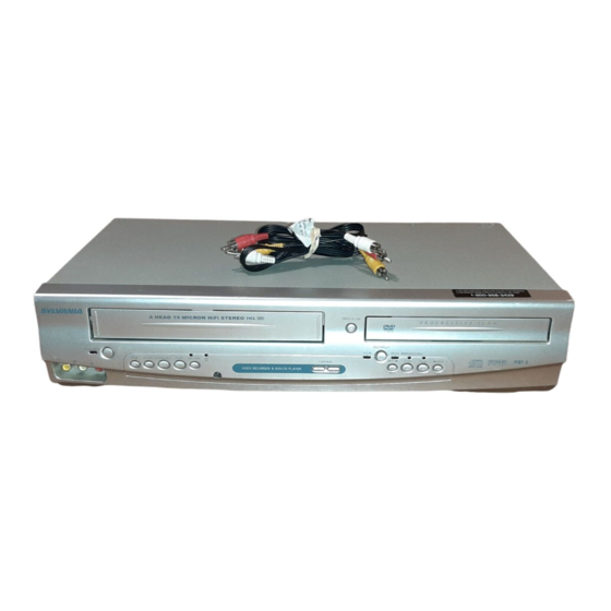
VIDEO CASSETTE RECORDER
DVC840G
POWER
REW
F.FWD
STOP/EJECT PLAY
REC/OTR
/
DVD PLAYER &
DVC865G
POWER
REW
F.FWD STOP/EJECT
PLAY
REC/OTR
OPEN/CLOSE
OUTPUT
VCR
DVD PROGRESSIVE SCAN
SKIP H
STOP
PLAY
G SKIP
CHANNEL
REV
FWD
When servicing the deck
mechanism, refer to MK14 Deck
Mechanism Section.
Deck Mechanism Part No.
DVC865G: N2460FL
DVC840G,DVC841G: N2440FL
OPEN/CLOSE
OUTPUT
VCR
DVD PROGRESSIVE SCAN
SKIP H
STOP
PLAY
G SKIP
CHANNEL
REV
FWD
DVC841G
POWER
REW
F.FWD
STOP/EJECT PLAY
REC/OTR
OPEN/CLOSE
OUTPUT
VCR
DVD PROGRESSIVE SCAN
SKIP
H
STOP
PLAY
G
SKIP
CHANNEL
REV
FWD
Advertisement
Table of Contents

Related Manuals for Sylvania DVC865G


Summary of Contents for Sylvania DVC865G
- Page 1 MK14 Deck I Preparation for Servicing Mechanism Section. I Adjustment Procedures I Schematic Diagrams Deck Mechanism Part No. I CBA’s I Exploded Views DVC865G: N2460FL I Parts List DVC840G,DVC841G: N2440FL DVD PLAYER & VIDEO CASSETTE RECORDER DVC865G OPEN/CLOSE OUTPUT...
- Page 2 IMPORTANT SAFETY NOTICE Proper service and repair is important to the safe, reliable operation of all Funai Equipment. The service procedures recommended by Funai and described in this service manual are effective methods of performing service operations. Some of these service special tools should be used when and as recommended.
-
Page 3: Table Of Contents
MAIN SECTION DVD PLAYER & VIDEO CASSETTE RECORDER DVC865G/DVC840G/DVC841G Main Section I Specifications I Preparation for Servicing I Adjustment Procedures I Schematic Diagrams I CBA’s I Exploded Views I Parts List TABLE OF CONTENTS Specifications ................1-1-1 Laser Beam Safety Precautions . -
Page 4: Specifications
4-2. Video S/N E-E Mode 4-3. Audio output E-E Mode 4-4. Audio S/N E-E Mode 5. Hi-Fi Audio [ DVC865G ] 5-1. Output SP Mode 5-2. Dynamic Range SP Mode 5-3. Freq. resp (6 dB B.W) 20 ~ 20 k SP Mode Note: Nominal specs represent the design specs. - Page 5 < DVD Section > Item Conditions Unit Nominal Limit 75 Ω load 1. Video Output ± 0.1 75 Ω load 2. Coaxial Digital Out mVpp ± 50 3. Audio (PCM) 1 kHz, 0 dB, 47k Ω load 3-1. Output Level Vrms 47k Ω...
-
Page 6: Laser Beam Safety Precautions
LASER BEAM SAFETY PRECAUTIONS This DVD player uses a pickup that emits a laser beam. Do not look directly at the laser beam coming from the pickup or allow it to strike against your skin. The laser beam is emitted from the location shown in the figure. When checking the laser diode, be sure to keep your eyes at least 30 cm away from the pickup lens when the diode is turned on. -
Page 7: Important Safety Precautions
IMPORTANT SAFETY PRECAUTIONS Product Safety Notice Also check areas surrounding repaired locations. J. Be careful that foreign objects (screws, solder Some electrical and mechanical parts have special droplets, etc.) do not remain inside the set. safety-related characteristics which are often not K. - Page 8 Safety Check after Servicing Examine the area surrounding the repaired location for damage or deterioration. Observe that screws, parts, and wires have been returned to their original positions. Afterwards, do the following tests and confirm the specified values to verify compliance with safety standards. 1.
-
Page 9: Standard Notes For Servicing
STANDARD NOTES FOR SERVICING Circuit Board Indications Pb (Lead) Free Solder 1. The output pin of the 3 pin Regulator ICs is When soldering, be sure to use the Pb free solder. indicated as shown. How to Remove / Install Flat Pack-IC Top View Bottom View 1. - Page 10 3. The flat pack-IC on the CBA is affixed with glue, so With Soldering Iron: be careful not to break or damage the foil of each 1. Using desoldering braid, remove the solder from pin or the solder lands under the IC when all pins of the flat pack-IC.
- Page 11 2. Installation With Iron Wire: 1. Using desoldering braid, remove the solder from 1. Using desoldering braid, remove the solder from all pins of the flat pack-IC. When you use solder the foil of each pin of the flat pack-IC on the CBA flux which is applied to all pins of the flat pack-IC, so you can install a replacement flat pack-IC more you can remove it easily.
- Page 12 Instructions for Handling Semi- conductors Electrostatic breakdown of the semi-conductors may occur due to a potential difference caused by electrostatic charge during unpacking or repair work. 1. Ground for Human Body Be sure to wear a grounding band (1 MΩ) that is properly grounded to remove any static electricity that may be charged on the body.
-
Page 13: Preparation For Servicing
PREPARATION FOR SERVICING How to Enter the Service Mode About Optical Sensors Caution: An optical sensor system is used for the Tape Start and End Sensors on this equipment. Carefully read and follow the instructions below. Otherwise the unit may operate erratically. What to do for preparation Insert a tape into the Deck Mechanism Assembly and press the [PLAY] button. -
Page 14: Cabinet Disassembly Instructions
CABINET DISASSEMBLY INSTRUCTIONS 1. Disassembly Flowchart Removal This flowchart indicates the disassembly steps to gain Remove/*Unhook/ Loc. Part Fig. Unlock/Release/ Note access to item(s) to be serviced. When reassembling, Unplug/Desolder follow the steps in reverse order. Bend, route, and dress the cables as they were originally. DVD Open/ [10] D6 *Desolder... - Page 15 5. Before installing the Deck Assembly, be sure to place the pin of LD-SW on Main CBA as shown in Fig. D6. Then, install the Deck Assembly while CN401 (S-3) aligning the hole of Cam Gear with the pin of LD- CN601 SW, the shaft of Cam Gear with the hole of LD-SW (S-3)
- Page 16 (S-7) (S-7) (S-7) (S-8) [8] VCR Chassis Unit Fig. D5 1-6-3 E8A00DC...
- Page 17 Cylinder Assembly FE Head ACE Head Assembly SW512 [9] Deck Assembly LD-SW (S-11) [11] Main CBA [9] Deck Assembly Cam Gear (S-9) [11] Main CBA Hole [10] DVD Shaft (S-10) Open/Close CBA Hole Desolder LD-SW Lead with [11] Main CBA blue stripe From From...
- Page 18 3. HOW TO EJECT MANUALLY 1. Remove the Top Case, Front Assembly and Top Bracket. 2. Remove four Screws (S-3) in Fig. D3. Do not disconnect connectors. 3. While lifting up the DVD Mechanism, rotate the roulette in the direction of the arrow as shown below. 4.
-
Page 19: Electrical Adjustment Instructions
ELECTRICAL ADJUSTMENT INSTRUCTIONS General Note: “CBA” is abbreviation for Head Switching Position “Circuit Board Assembly.” Adjustment NOTE: Purpose: To determine the Head Switching position 1. Electrical adjustments are required after replacing during playback. circuit components and certain mechanical parts. Symptom of Misadjustment: May cause Head It is important to do these adjustments only after Switching noise or vertical jitter in the picture. -
Page 20: How To Initialize The Dvd Player & Vcr
HOW TO INITIALIZE THE DVD PLAYER & VCR To put the program back at the factory-default, initialize the DVD player & VCR as the following procedure. < DVD Section > 1. Press [DVD], [1], [2], [3], [4], and [DISPLAY] buttons on the remote control unit in that order. Fig. -
Page 21: Firmware Renewal Mode
FIRMWARE RENEWAL MODE 1. Turn the power on and remove the disc on the tray. " ******* " differs depending on the models. 2. To put the DVD player into version up mode, press [DVD], [9], [8], [7], [6], and [SEARCH MODE] F/W Version Up Mode Model No : ******* VERSION : *.**... -
Page 22: Function Indicator Symbols
FUNCTION INDICATOR SYMBOLS Note: If a mechanical malfunction occurs, the power is turned off. When the power comes on again after that by pressing [POWER] button, an error message is displayed on the TV screen for 5 seconds. Cause Indicator Active When reel or capstan mechanism is not “EJECT A R”... -
Page 23: Block Diagrams
BLOCK DIAGRAMS <VCR SECTION> Servo / System Control Block Diagram 1-11-1 E8A00BLS... - Page 24 Video Block Diagram 1-11-2 E8A00BLV...
- Page 25 Audio Block Diagram ( DVC865G ) E8A00BLA 1-11-3...
- Page 26 Audio Block Diagram ( DVC840G ,DVC841G) 1-11-4 E8A02BLA...
- Page 27 Hi-Fi Audio Block Diagram (DVC865G) E8A00BLH 1-11-5...
- Page 28 Power Supply Block Diagram 1-11-6 E8A00BLP...
- Page 29 BLOCK DIAGRAMS <DVD SECTION> DVD System Control / Servo Block Diagram 1-11-7 E8A00BLSD...
- Page 30 Digital Signal Process Block Diagram 1-11-8 E8A00BLD...
- Page 31 DVD Video / Audio Block Diagram 1-11-9 E8A00BLVD...
-
Page 32: Schematic Diagrams / Cba's And Test Points
SCHEMATIC DIAGRAMS / CBA’S AND TEST POINTS Standard Notes WARNING Many electrical and mechanical parts in this chassis have special characteristics. These characteristics often pass unnoticed and the protection afforded by them cannot necessarily be obtained by using replacement components rated for higher voltage, wattage, etc. - Page 33 LIST OF CAUTION, NOTES, AND SYMBOLS USED IN THE SCHEMATIC DIAGRAMS ON THE FOLLOWING PAGES: 1. CAUTION: FOR CONTINUED PROTECTION AGAINST FIRE HAZARD, REPLACE ONLY WITH THE SAME TYPE FUSE. ATTENTION: POUR UNE PROTECTION CONTINUE LES RISQES D'INCELE N'UTILISER QUE DES FUSIBLE DE MÊME TYPE. RISK OF FIRE-REPLACE FUSE AS MARKED.
- Page 34 Main 1/8 Schematic Diagram < VCR Section > E8A00SCM1 1-12-3...
- Page 35 Main 2/8 & Sensor Schematic Diagram < VCR Section > E8A00SCM2 1-12-4...
- Page 36 Main 3/8 Schematic Diagram < VCR Section > E8A00SCM3 1-12-5...
- Page 37 Main 4/8 Schematic Diagram < VCR Section > E8A00SCM4 1-12-6...
- Page 38 Main 5/8 Schematic Diagram < VCR Section > 1-12-7 E8A00SCM5...
- Page 39 Main 6/8 & DVD Open/Close Schematic Diagram < VCR Section > E8A00SCM6 1-12-8...
- Page 40 Main 7/8 Schematic Diagram < VCR Section > CAUTION ! CAUTION ! NOTE: For continued protection against fire hazard, The voltage for parts in hot circuit is measured using Fixed voltage (or Auto voltage selectable) power supply circuit is used in this unit. If Main Fuse (F1001) is blown , check to see that all components in the power supply replace only with the same type fuse.
- Page 41 Main 8/8 Schematic Diagram < VCR Section > ( DVC865G ) E8A00SCM8 1-12-10...
- Page 42 DVD Main 1/3 Schematic Diagram < DVD Section > 1 NOTE: Either IC461 or IC462 is used for DVD MAIN CBA UNIT. 1-12-11 E8A00SCD1...
- Page 43 DVD Main 2/3 Schematic Diagram < DVD Section > E8A00SCD2 1-12-12...
- Page 44 DVD Main 3/3 Schematic Diagram < DVD Section > E8A00SCD3 1-12-13...
- Page 45 Main CBA Top View Because a hot chassis ground is present in the power CAUTION ! DVD Open/Close CAUTION ! For continued protection against fire hazard, supply circut, an isolation transformer must be used. Fixed voltage (or Auto voltage selectable) power supply circuit is used in this unit. CBA Top View Also, in order to have the ability to increase the input replace only with the same type fuse.
- Page 46 Main CBA Bottom View Because a hot chassis ground is present in the power CAUTION ! CAUTION ! supply circut, an isolation transformer must be used. Fixed voltage (or Auto voltage selectable) power supply circuit is used in this unit. For continued protection against fire hazard, Also, in order to have the ability to increase the input If Main Fuse (F1001) is blown , check to see that all components in the power supply...
-
Page 47: Waveforms
WAVEFORMS NOTE: Input VCR: COLOR BAR SIGNAL (WITH 1KHz AUDIO SIGNAL) (WF1~WF3, WF10~WF15) DVD: POWER ON (STOP) MODE (WF4~WF6) CD: 1kHz PLAY (WF7~WF9) TP751 Pin 8 of CN1601 Pin 12 of CN1601 V-OUT E-E 0.2V 20µs AUDIO (L) 0.5ms VIDEO-Y 0.2V 20µs TP751... - Page 48 NOTE: Input VCR: COLOR BAR SIGNAL (WITH 1KHz AUDIO SIGNAL) (WF1~WF3, WF10~WF15) DVD: POWER ON (STOP) MODE (WF4~WF6) CD: 1kHz PLAY (WF7~WF9) WF10 WF13 Pin 1 of TU701 Pin 11 of TU701 MOD-A 0.5V 0.2ms PLL-DATA WF11 WF14 Pin 5 of TU701 Pin 13 of TU701 MOD-V 0.5V...
-
Page 49: Wiring Diagram < Vcr Section
WIRING DIAGRAM < VCR SECTION > 1-14-1 E8A00WI... -
Page 50: Wiring Diagram < Dvd Section
WIRING DIAGRAM < DVD SECTION > E8A00WID 1-14-2... -
Page 51: System Control Timing Charts
SYSTEM CONTROL TIMING CHARTS < VCR Section > Mode SW: LD-SW LD-SW Position detection A/D Input voltage Limit Symbol (Calculated voltage) 3.76 V ~ 4.50 V (4.12 V) 4.51 V ~ 5.00 V (5.00 V) 0.00 V ~ 0.25 V (0.00 V) 1.06 V ~ 1.50 V (1.21 V) 0.66 V ~ 1.05 V (0.91 V) 1.99 V ~ 2.60 V (2.17 V) - Page 52 Still/Slow Control Frame Advance Timing Chart 1) SP Mode 18 RF-SW The first rise of RF-SW after a rise in F-AD signal F-AD (Internal Signal) "H" "H" "Z" C-DRIVE "L" "L" Stop detection (T2) Acceleration Detection (T1) Slow Tracking Value PB CTL Reversal Limit Value 20ms...
- Page 53 2) LP/SLP Mode 18 RF-SW The first rise of RF-SW after a rise in F-AD signal F-AD (Internal Signal) "H" "H" "Z" C-DRIVE "L" "L" Stop detection (T2) Acceleration Detection (T1) Slow Tracking Value PB CTL Reversal Limit Value 20ms 27 C-F/R 79 H-A-SW 78 C-ROTA...
- Page 54 EJECT ST-S/ END-S "OFF" CASS.LOAD LD-FWD 0.2S LD-REV 0.7S LD-FWD 0.4S LD-FWD 0.2S LD-REV 0.2S LD-FWD 0.5S LD-REV STOP(A) PLAY LD-FWD PLAY LD-FWD LD-REV 0.2S LD-FWD PLAY PLAY PAUSE (SLOW) LD-FWD STILL(SLOW) PLAY LD-REV 0.2S LD-FWD PLAY STOP /EJECT LD-REV STOP(A) Fig.
- Page 55 STOP(A) STOP STOP(A) STOP LD-REV LD-REV 0.2S 0.2S LD-FWD LD-FWD STOP STOP /EJECT /EJECT 1.0S 1.0S LD-FWD LD-FWD 0.5S 0.5S LD-REV LD-REV STOP(A) STOP(A) LD-REV LD-REV 0.2S 0.2S LD-FWD LD-FWD STOP STOP /EJECT LD-REV /EJECT LD-REV 1.0S 1.0S LD-FWD LD-FWD 0.5S 0.5S LD-REV...
- Page 56 < DVD Section > Tray Close ~ Play / Play ~ Tray Open Tray Disc Disc Tray Play Close Rotation Stop Open 3.3V Tray IN (TL221) Sled Drive 1.65V (TP303) Disc Drive 1.65V (TP301) 1.65V Focus Drive (TP304) Tracking Drive 1.65V (TP302) 1-15-6...
-
Page 57: Ic Pin Function Descriptions
Function Name Level Comparison Chart of Models and Marks YCA IC Control OUT YCA-SDA Data Model Mark YCA IC Control DVC865G OUT YCA-CS Chip Select DVC840G DVC841G Not Used IC501 (SERVO/SYSTEM CONTROL/OSD) Video Head OUT RF-SW Switching “H” ≥ 4.5 V, “L” ≤ 1.0 V... - Page 58 Signal Active Signal Active Mark Function Mark Function Name Level Name Level Sub Clock Amp. Output OUT XO Output 32.768 OUT CTL Control Signal for Test Point Operation Audio Mode HiFi/NOR- IN SXI Mode Selecting Input (HiFi = “L” Input Signal / Normal = “H”) Composite Not Used...
- Page 59 Signal Active Mark Function Name Level REC Mode REC- LED Signal LED-L Output REC Mode REC- LED Signal LED-L Output TIMER Mode TIMER- LED Signal LED-L Output TIMER Mode TIMER- LED Signal LED-L Output Color Phase Rotary OUT C-ROTA Changeover Signal Video Head OUT H-A-SW...
-
Page 60: Lead Identifications
LEAD IDENTIFICATIONS KRA103M-AT/P 2SC1815-Y(TE2 F T) KIA4558P/P KRC103M-AT/P KTC3198-Y-AT/P KTA-1266-GR-AT/P KTC3203-Y-AT/P KTA1267-Y-AT/P 2SC2001-T-A-K KTC3193-Y-AT/P KTC3199-(Y,BL)-AT/P E C B E C B MM1637XVBE PS2561A-1(W) 1: Anode 2: Cathode 3: Emitter 4: Collector PQ1LAX95MSPQ CD4053BNSR RN1511(TE85R.F) 1: VREF 2: GND 3: VC 4: VIN 5: VOUT B1 E B2... -
Page 61: Exploded Views
EXPLODED VIEWS Cabinet 2L071 2L071 2L071 2L021 2L021 2L071 2L021 L0-9 2L082 L0-9 W004 2L021 2L062 Sensor CBA 2L051 2B11 DVD Main CBA Unit Main CBA 2L012 Sensor CBA These FFC cables are included 2B16 in 1B2 (DVD mechanism). 2B15 2L051 2B15 2L022... - Page 62 Packing Unit 1-18-2 E8A61PEX...
-
Page 63: Mechanical Parts List
X20# OWNERS MANUAL E8A04UD 1VMN22700 NOTE: Parts that are not assigned part numbers (---------) are not available. Comparison Chart of Models and Marks Model Mark DVC865G DVC840G DVC841G Ref. No. Mark Description Part No. FRONT ASSEMBLY H9802UD 1VM220380 FRONT ASSEMBLY E8A02UD... -
Page 64: Electrical Parts List
Comparison Chart of Models and Marks C329 CHIP CERAMIC CAP . B K 0.01µF/50V CHD1JKB0B103 Model Mark C330 ELECTROLYTIC CAP . 1µF/50V M H7 CE1JMAVSL1R0 DVC865G C331 CHIP CERAMIC CAP . B K 0.01µF/50V CHD1JKB0B103 DVC840G C332 ELECTROLYTIC CAP . 1µF/50V M H7 CE1JMAVSL1R0 DVC841G C333 CHIP CERAMIC CAP . - Page 65 Ref. No. Mark Description Part No. Ref. No. Mark Description Part No. C454 ELECTROLYTIC CAP . 1µF/50V M H7 CE1JMAVSL1R0 C540 CHIP CERAMIC CAP . B K 0.01µF/50V CHD1JKB0B103 C455 ELECTROLYTIC CAP . 22µF/6.3V M H7 CE0KMAVSL220 C541 CHIP CERAMIC CAP . F Z 0.1µF/50V CHD1JZB0F104 C456 ELECTROLYTIC CAP .
- Page 66 Ref. No. Mark Description Part No. Ref. No. Mark Description Part No. C1441 CHIP CERAMIC CAP . B K 0.33µF/10V CHD1AKB0B334 IC1001 PHOTOCOUPLER PS2561A-1(W) QPEWPS2561A1 C1442 ELECTROLYTIC CAP . 1000µF/6.3V M CE0KMASDL102 IC1002 VOLTAGE REGULATOR QSZBA0TSH053 C1461 ELECTROLYTIC CAP . 1µF/50V M H7 CE1JMAVSL1R0 PQ1LAX95MSPQ C1462...
- Page 67 Ref. No. Mark Description Part No. Ref. No. Mark Description Part No. CHIP RES. 1/10W J 8.2k Ω Q1351 TRANSISTOR KTC3199-Y-AT/P NQSYKTC3199P R409 RRXAJB5Z0822 CHIP RES. 1/10W J 12k Ω Q2002 TRANSISTOR KTC3199-Y-AT/P NQSYKTC3199P R410 RRXAJB5Z0123 CHIP RES. 1/10W J 330k Ω Q2013 TRANSISTOR KTC3199-Y-AT/P NQSYKTC3199P...
- Page 68 Ref. No. Mark Description Part No. Ref. No. Mark Description Part No. CHIP RES. 1/10W J 390k Ω CARBON RES. 1/4W J 1.2k Ω R541 RRXAJB5Z0394 R1032 RCX4JATZ0122 CARBON RES. 1/4W J 270 Ω CARBON RES. 1/4W J 680k Ω R542 RCX4JATZ0271 R1034...
- Page 69 DVD OPEN/CLOSE CBA Ref. No. Mark Description Part No. CARBON RES. 1/4W J 180 Ω R2054 RCX4JATZ0181 Ref. No. Mark Description Part No. CHIP RES. 1/10W J 10k Ω R2055 RRXAJB5Z0103 DVD OPEN/CLOSE CBA (MCV-C) ---------- CHIP RES. 1/10W J 10k Ω R2056 RRXAJB5Z0103 Consists of the following:...
- Page 70 DVC865G/DVC840G/DVC841G E8A00/02/04UD 2006-03-27...
- Page 71 This service manual supplement is for the DVC865G(E8C00UD) ,DVC840G(E8C02UD) , DVC841G(E8C04UD) model, which is different from J U L Y 2 0 0 6 the DVC865G(E8A00UD) ,DVC840G(E8A02UD) , DVC841G(E8A04UD) model. "E8C00UD" Rating Label For the DVC865G(E8C00UD) ,DVC840G(E8C02UD) , DVC841G(E8C04UD) model, the letter (E8C00UD)
- Page 72 Different parts from the DVC865G(E8A00UD) model DVC865G (E8C00UD) Ref. No. Description Part No. MECHANICAL PARTS A10# RATING LABEL(U) E8C00UD ---------- X20# OWNERS MANUAL E8A00UD 1VMN21872A ELECTRICAL PARTS DVD MAIN CBA UNIT N7CFAKUP Different parts from the DVC840G(E8A02UD) model DVC840G (E8C02UD) Ref.
Need help?
Do you have a question about the DVC865G and is the answer not in the manual?
Questions and answers
dvd tray won't come out when I press the open/close/eject button
The DVD tray on the Sylvania DVC865G may not open when pressing the open/close/eject button if the player is in firmware version up mode. In this mode, normal button functions are disabled, and the tray only opens automatically during specific steps of the update process. To exit this mode and restore normal operation, unplug the AC cord, then plug it back in and turn the power on.
This answer is automatically generated