Table of Contents
Advertisement
Quick Links
Advertisement
Table of Contents

Summary of Contents for EMTOP SOM-IMX8M-MINI
-
Page 1: Som-Imx8M-Mini
SOM-IMX8M-MINI... -
Page 2: Table Of Contents
Contents SOM-IMX8M-MINI..........................1 1. General..........................3 2. Features..........................4 2.1 SOM-IMX8M-MINI.....................4 2.2 DEV-IMX8M-MINI...................... 5 3. Application..........................6 4. Mechanical Dimension......................7 5. Electrical Characteristics....................8 5.1 Working Temperature....................8 6. Hardware Overview......................8 6.1 System Components....................8 6.2 Functional Block Diagrams..................10 7. Interface Description......................11 7.1 BTB ON Connector....................11... -
Page 3: General
On-board up to 2GB DDR4, up to 64GB eMMC and a WiFi / Bluetooth module, and with MIPI DSI display driver, MIPI CSI camera receiver, flexible audio interfaces and comprehensive communication features. The SOM-IMX8M-MINI Module is a fully-integrated system that helps you build your professional embedded systems rapidly. -
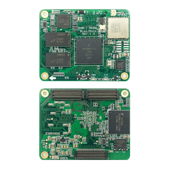
Page 4: Features
2. Features 2.1 SOM-IMX8M-MINI Picture2.1 Top side of SOM-IMX8M-MINI Picture2.2 Bottom side of SOM-IMX8M-MINI Up to Quad-core ARM Cortex-A53 o 64-bit Armv8-A architecture o Target frequency up to 1.8GHz 2D/3D GC520L o Media Processing Engine (MPE) with NEON technology o Floating Point Unit (FPU) with support of the VFPv4-D16 architecture... -
Page 5: Dev-Imx8M-Mini
One Cortex-M4 up to 400MHz Wi-Fi 1x1 (802.11b/g/n/ac 2.4/5GHz) Bluetooth 5.0 From 8 to 64GB eMMC Up to2GB DDR4 64M bit Quad SPI Flash on-board 3*60Pin 0.5mm pitch BTB connectors Up to 75xGPIO (including SPI,I2C,PWM,UART,SAI, and SDIO) 2.2 DEV-IMX8M-MINI Picture2.3 DEV-IMX8M-MINI ... -
Page 6: Application
USB Touch x 1 MIPI-CSI x 1 Fan 5V port x 1 MIPI-DSI x 1 Buzzer x 1 SIM Card x 1 TF Card x 1 Mini PCIE Interface x 1, For 4G module and PCIE module ... -
Page 7: Mechanical Dimension
4. Mechanical Dimension Size: 50 x 40 x 7.3 mm PCB Parameter:8 layer design, lead-free soldering process Weight: 12g Picture4.1 Mechanical Dimension of Top side Picture4.2 Mechanical Dimension of Bottom side... -
Page 8: Electrical Characteristics
5. Electrical Characteristics 5.1 Working Temperature Table5.1 Working Temperature Minimum Operating Temperature Operating Temperature Specification (℃) (℃) Commercial Grade Industrial Grade -40 +85 Note: A heat sink may need for some applications 6. Hardware Overview 6.1 System Components Table6.1 Hardware Overview Feature Details i.MX8M MINI SOC... - Page 9 • On-chip RAM (256KB + 32KB) Memory and storage • 2GB DDR4 SDRAM (32-bit bus width) • 1200MHz maximum DDR clock DDR SDRAM • Interfaces directly to the iMX8M MIPI build-in DDR controller • 8GB NAND eMMC flash memory • 8-bits MMC mode eMMC •...
-
Page 10: Functional Block Diagrams
6.2 Functional Block Diagrams The following figure is a functional block diagram of the SOM-IMX8M-MINI: Picture6.1 Functional Block Diagrams Picture6.2 i.MX 8M Mini system block diagram... -
Page 11: Interface Description
7. Interface Description 7.1 BTB ON Connector The BTB connector mounted on SOM is MB250-G60S-B1R supplied by MTCONN. The specification of the connector is: Picture7.1 Connector Specifications For SOM The recommended BTB connector can be mounted on baseboard is MB250-G60P-B1R supplied by MTCONN, an equal parameters BTB connector can be used instead. -
Page 12: Wifi/Bt Antenna Connector
7.2 WiFi/BT Antenna Connector The antenna connector mounted on SOM is Ultra Small Surface Mount Coaxial Connector, the detail of the connector is as following: Picture7.3 Specifications For UFL... -
Page 13: Pinout Description Table
8. Pinout Description Table Picture8.1 Assemble BTB on bottom side of SOM-IMX8M-MINI... - Page 14 5V_IN DSI_DN0 DSI_DP0 DSI_DN1 DSI_CKN DSI_DP1 DSI_CKP DSI_DN2 DSI_DN3 DSI_DP2 DSI_DP3 CSI_DN0 CSI_DN1 CSI_DP0 CSI_DP1 CSI_CKN CSI_DN2 CSI_CKP CSI_DP2 CSI_DN3 PCIE_RX_N CSI_DP3 PCIE_RX_P PCIE_TX_N PCIE_CLK_N PCIE_TX_P PCIE_CLK_P USB1_DN USB1_DP UART4_TXD UART4_RXD USB2_DN USB1_ID VDDUSB1_5V USB2_DP VDDUSB2_5V BOOT_MODE0 BOOT_MODE1 Picture8.2 Pin out of J1 Table8.1 Pin Definition of J1 Number Signal...
- Page 15 Number Signal Power Logic Input/Output CPU Ball Note CSI_DN1 MIPI CSI Input CSI_DP0 MIPI CSI Input CSI_DP1 MIPI CSI Input CSI_CKN MIPI CSI Input CSI_DN2 MIPI CSI Input CSI_CKP MIPI CSI Input CSI_DP2 MIPI CSI Input CSI_DN3 MIPI CSI Input PCIE_RX_N PCIe Input...
- Page 16 Picture8.3 Pin out of J2 Table8.2 Pin Definition of J2 Number Signal Power Logic Input/Output CPU Ball Note SAI5_MCLK 3.3V In/Out AD15 SAI1_RXD0 3.3V In/Out AG15 Boot CFG 0 SAI1_RXD1 3.3V In/Out AF15 Boot CFG 1 SAI5_RXD0 3.3V In/Out AD18 SAI1_RXFS 3.3V In/Out...
- Page 17 Number Signal Power Logic Input/Output CPU Ball Note SD2_DATA1 NVCC_SD2 In/Out AB24 SAI1_TXD2 3.3V In/Out AG21 Boot CFG 10 SD2_CMD NVCC_SD2 In/Out SAI1_TXD3 3.3V In/Out AF21 Boot CFG 11 SAI1_TXD4 3.3V In/Out AG22 Boot CFG 12 SAI1_TXD6 3.3V In/Out AG23 Boot CFG 14 SAI1_TXD5 3.3V...
- Page 18 I2C4_SDA ESPI2_MISO I2C4_SCL ESPI2_MOSI ESPI2_SCLK I2C2_SDA ESPI2_SS0 I2C2_SCL PWR_KEY I2C3_SDA RESET I2C3_SCL UART3_RXD UART3_RTS VDD_3V3 UART3_TXD SAI3_TXC UART3_CTS SAI3_TXD SAI3_RXC GPIO1_IO15 SAI3_RXD GPIO1_IO14 SAI3_RXFS SAI3_TXFS SPDIF_EXT_CLK SAI3_MCLK SPDIF_RX SPDIF_TX GPIO1_IO13 GPIO1_IO08 GPIO1_IO12 GPIO1_IO09 GPIO1_IO10 SAI5_RXD2 GPIO1_IO06 SAI5_RXC GPIO1_IO05 SAI5_RXFS GPIO1_IO01 SAI5_RXD1 SAI5_RXD3 UART2_TXD...
- Page 19 Number Signal Power Logic Input/Output CPU Ball Note SAI3_TXC 3.3V In/Out UART3_CTS 3.3V In/Out SAI3_TXD 3.3V In/Out SAI3_RXC 3.3V In/Out GPIO1_IO15 3.3V In/Out SAI3_RXD 3.3V In/Out GPIO1_IO14 3.3V In/Out SAI3_RXFS 3.3V In/Out SAI3_TXFS 3.3V In/Out SPDIF_EXT_CLK 3.3V In/Out SAI3_MCLK 3.3V In/Out SPDIF_RX 3.3V...
-
Page 20: Power Supply And System Resets
9. Power Supply And System Resets 9.1 Power Source The SOM-IMX8M-MINI have built-in power management function, so it is only need to provide a +5V power source to the SOM-IMX8M-MINI via the 5V input pins of the J1 connector. The power consumption is requested 2A/5V(10 W) at least for the IMX8M-MINI-SOM board to be working properly. -
Page 21: System Resets
10. System Resets 10.1 Power-on Reset This type of reset occurs when the power is initially applied to the SOM-IMX8M-MINI. As the supply voltage rises, the on-board PMIC holds the i.MX 8M MINI in reset until all the processor power supply voltages have risen above the appropriate voltage thresholds (90% of the nominal values). -
Page 22: Trace Impedance Recommendations
12. Trace impedance recommendations The following table lists the recommended impedance for high-speed signals on the baseboard. Table12.1 Trace Impedance Recommendation Signal group Impedance PCB manufacture tolerance All single-ended signal,unless 50 Ohm single-ended +/-10% specified PCIe TX/RX data pair 85 Ohm differential +/-10% PCIe differential clocks 100 Ohm differential... - Page 23 DSI_DN3 511.74 483.98 DSI_DP3 516.23 483.98 PCIe PCIE_CLK_N 495.48 477.35 PCIE_CLK_P 495.7 516.73 PCIE_RX_N 475.14 457.67 PCIE_RX_P 487.48 497.04 PCIE_TX_N 623.25 634.84 PCIE_TX_P 649.18 674.21 USB1 USB1_DN 647.78 654.52 USB1_DP 652.37 693.9 USB2 USB2_DN 676.18 693.89 USB2_DP 680.79 733.26 Ethernet ETH_TRN0 246.14 172.62...
-
Page 24: Circuit Example
14. Circuit Example 14.1 Reset In For the reset pin J3.16, a reset button to pull this pin to ground to reset core board is necessary, the ESD component and bypass capacitor is used according to the actual design, a resistor pull up to power supply is installed on SOM board, so not any resistors pull up/down is need. -
Page 25: Giga Ethernet
TF single on BTB connector: Connected to uSDHC2 On-board QSPI Flash: Connected to QSPI, 1.8V 64M bit QSPI flash, W25Q64FW i.MX8M Mini ROM Fuse Address 0x470[15:8] BOOT_CFG[15] BOOT_CFG[14] BOOT_CFG[13] BOOT_CFG[12] BOOT_CFG[11] BOOT_CFG[10] BOOT_CFG[9] BOOT_CFG[8] 0x470[15:8] 001 - SD/eSD Port Sel ect: SD Loopba ck Cl ock Power Cycl e Ena bl e 00 - uSDHC1... -
Page 26: Tf Card
JTRJ45-4118NLF 100Mbps: Green 1Gbps :Orange ETH_TRP0 LED_1000 TD1+ GRL+/OG- ETH_TRN0 LED_10_100 TD1- GRL-/OG+ ETH_TRP1 ETH_2V5 TD2+ ETH_TRN1 TD2- ETH_TRP2 LED_ACT RD1+ Y EL- ETH_TRN2 RD1- Y EL+ ETH_TRP3 RD2+ ETH_TRN3 RD2- ETH_2V5 Not Installed 0.1uF 0.1uF 0.001uF 15pF 15pF 15pF 15pF 2KV,X7R For EMC Test... -
Page 27: Pcie Clock
J2.60 MMBT2222A-7-F BAT60A E6327 0.1uF Picture14.8 Power supply for SOM-IMX8M-MINI GPIO1_IO05: During reset: output high without PU/PD; After reset: input with PU SAI5_CLK: During reset: input without PU/PD; After reset: input with PD 14.7 PCIe Clock In order to boot up the system smoothly, a PCIe differential clock input is necessary. For example, a 100MHz differential clock input to J1.43 and J1.45 on DEV-IMX8M-MINI is design to complete...
Need help?
Do you have a question about the SOM-IMX8M-MINI and is the answer not in the manual?
Questions and answers