Table of Contents
Advertisement
Quick Links
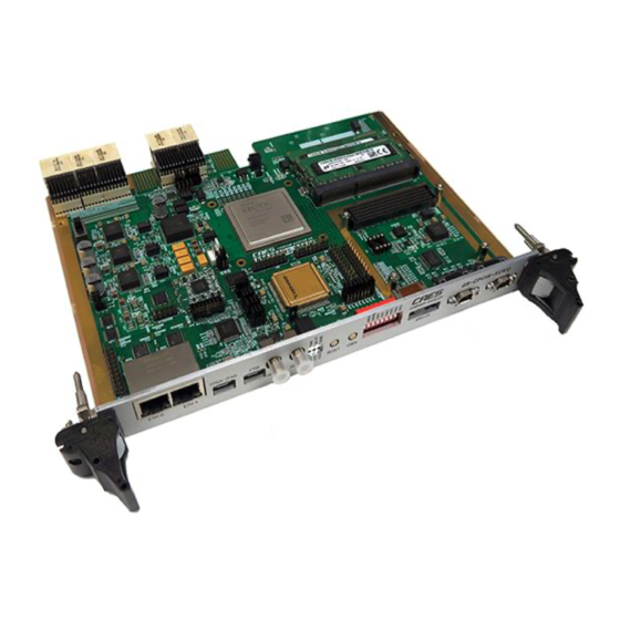
GR-CPCIS-XCKU Development Board
GR-CPCIS-XCKU
Baseline features
The GR-CPCIS-XCKU is an FPGA development
board. Its cutting-edge technology allows the
development of next-generation system on
chips and its interfaces are particularly suited
to emulate space applications.
This board implements a Xilinx Ultrascale
FPGA, in a 1517 ball-grid-array package. The
board was initially designed to use a XCKU060
sized device but is compatible with larger
devices of the same series with the same
footprint.
Optionally, the board also features a GR716
rad-hard microcontroller which can act as the
FPGA supervisor for scrubbing and
programming.
The GR-CPCIS-XCKU is a 1 slot, 6U high
board with a CPCI-S backplane format, and
can be used stand alone on the bench top, or
installed in a CPCI-Serial rack
The GR-CPCIS-XCKU includes:
•
Xilinx XCKU, in 1517 pin FCBGA package.
•
GR716 microcontroller. - Optional
•
FPGA interface to DDR3 SDRAM via two
SODIMM connectors.
•
SPI flash for FPGA configuration (512
Mbit), for GR716 boot (256 Mbit), and for
data (256 Mbit). The FPGA has also access
to two NVM: 512 Mbit SPI and Parallel
Flash memory (40 bit wide)
•
FMC Mezzanine expansion connector.
•
Scrubbing interface for FPGA. Available
also without the GR716.
•
2×10 connector to interface with a GR-
ACC-6U_6UART breakout board providing
access to 6 UARTS (or 16 GPIOs).
This board design is part of a project that has received funding from the European
Union's Horizon 2020 research and innovation programme under Grant Agree-
ment No 869945.
GR-CPCIS-XCKU-DSUM
Feb 2022, Version 1.2
Front Panel interfaces
•
2x RJ45 to FPGA via magnetics and Gbit
Ethernet transceivers. RGMII interface to
FPGA
•
1x eSATA for SpaceFibre to FPGA via CML
redriver.
•
2x
MDM9
for
SpaceWire
transceivers/repeaters to FPGA.
•
Status LEDs, push-buttons and switches
•
2xSMA or 2xSMB for PPS time distribution to
FPGA.
•
2xUSB ports for:
JTAG access to FPGA and FMC
o
(separate chains)
GR716 debug UART and two FPGA
o
UARTs
Backplane interfaces
•
8 x SpaceFibre for full-mesh interconnect
using FPGA GTH banks
•
8 x SpaceWire for dual-star interconnect
•
Dual-redundant CAN-bus to FPGA and/or
GR716 via two or four transceivers
•
SGPIO and I2C connected to FPGA with
jumper-configurable pull-ups
•
12V supply from backplane that can be turned
off by the external input PS_ON#
•
Other utility signals connected to the FPGA
Kungsgatan 12 | SE-411 19 Goteborg | Sweden
+46 31 7758650 | www.caes.com/gaisler
via
LVDS
© Cobham Gaisler AB
Advertisement
Table of Contents

Summary of Contents for CAES GR-CPCIS-XCKU
- Page 1 FPGA supervisor for scrubbing and programming. Front Panel interfaces The GR-CPCIS-XCKU is a 1 slot, 6U high • 2x RJ45 to FPGA via magnetics and Gbit board with a CPCI-S backplane format, and Ethernet transceivers.
-
Page 2: Table Of Contents
List of Headers ........................50 List of Oscillators, Switches and LED's ................51 © Cobham Gaisler AB Document Data Sheet & User Manual Kungsgatan 12 | SE-411 19 Goteborg | Sweden Feb 2022, Version 1.2 +46 31 7758650 | www.caes.com/gaisler... -
Page 3: Introduction
GR-CPCIS-XCKU INTRODUCTION Scope of the Document This document provides a Data Sheet & User Manual for the GR-CPCIS-XCKU Development and Demonstration board. The work has been performed by Cobham Gaisler AB, Göteborg, Sweden. Reference Documents The following documents are referred as they contain relevant information: GR-CPCIS-XCKU Board_schematic.pdf, Schematic... -
Page 4: Introduction
To Be Defined INTRODUCTION Overview This document describes the GR-CPCIS-XCKU Development Board. This equipment is a 1 slot, 6U high board with a CPCI-S backplane format. It can be used stand alone or it can be installed in a CPCI-Serial rack. - Page 5 • on-board regulators converting from VIN to various on-board voltages • switches and headers for bootstrap and configuration settings © Cobham Gaisler AB Document Data Sheet & User Manual Kungsgatan 12 | SE-411 19 Goteborg | Sweden Feb 2022, Version 1.2 +46 31 7758650 | www.caes.com/gaisler...
- Page 6 GR-CPCIS-XCKU GR-CPCIS-XCKU Main Board Figure 2 © Cobham Gaisler AB Document Data Sheet & User Manual Kungsgatan 12 | SE-411 19 Goteborg | Sweden Feb 2022, Version 1.2 +46 31 7758650 | www.caes.com/gaisler...
-
Page 7: Handling
20°C. All devices are standard commercial types, intended for use over the standard commercial operating temperature range (0 to 70ºC). © Cobham Gaisler AB Document Data Sheet & User Manual Kungsgatan 12 | SE-411 19 Goteborg | Sweden Feb 2022, Version 1.2 +46 31 7758650 | www.caes.com/gaisler... -
Page 8: Board Design
GR-CPCIS-XCKU BOARD DESIGN Board Block Diagram GR-CPCIS-XCKU Board Block Diagram Figure 3 Board provides the electrical functions and interfaces as represented in the GR-CPCIS-XCKU block diagram, Figure 3. © Cobham Gaisler AB Document Data Sheet & User Manual Kungsgatan 12 | SE-411 19 Goteborg | Sweden Feb 2022, Version 1.2... -
Page 9: Board Mechanical Format
FPGA version in a CNA1509 package instead of the commercial FFVA1517 package. © Cobham Gaisler AB Document Data Sheet & User Manual Kungsgatan 12 | SE-411 19 Goteborg | Sweden Feb 2022, Version 1.2 +46 31 7758650 | www.caes.com/gaisler... - Page 10 GTH banks Q225, Q226, Q227, Q228 provide high speed transceiver links to the CPCI-S backplane. © Cobham Gaisler AB Document Data Sheet & User Manual Kungsgatan 12 | SE-411 19 Goteborg | Sweden Feb 2022, Version 1.2 +46 31 7758650 | www.caes.com/gaisler...
-
Page 11: Gr716 Microcontroller
GPIO to Power Circuits to control the enabling of the +12V FMC power supply GR716 Interfaces Figure 5 © Cobham Gaisler AB Document Data Sheet & User Manual Kungsgatan 12 | SE-411 19 Goteborg | Sweden Feb 2022, Version 1.2 +46 31 7758650 | www.caes.com/gaisler... - Page 12 GPIO Header GPIO39 GPIO40 GPIO Header GPIO40 GPIO41 GPIO42 GPIO43 GPIO Header GPIO43 © Cobham Gaisler AB Document Data Sheet & User Manual Kungsgatan 12 | SE-411 19 Goteborg | Sweden Feb 2022, Version 1.2 +46 31 7758650 | www.caes.com/gaisler...
-
Page 13: Memory
512 Mbit SPI memory (Cypress, S25FL512SAGN in SOIC-16 package) for GR716-data non-volatile memory © Cobham Gaisler AB Document Data Sheet & User Manual Kungsgatan 12 | SE-411 19 Goteborg | Sweden Feb 2022, Version 1.2 +46 31 7758650 | www.caes.com/gaisler... -
Page 14: Board Interfaces
The Front Panel SPFI connections are buffer with a DS80PCI102SQ/NOPB CML re-driver circuit. © Cobham Gaisler AB Document Data Sheet & User Manual Kungsgatan 12 | SE-411 19 Goteborg | Sweden Feb 2022, Version 1.2 +46 31 7758650 | www.caes.com/gaisler... - Page 15 FPGA cannot be used for these links. SPW fail-safe RX network Figure 8 © Cobham Gaisler AB Document Data Sheet & User Manual Kungsgatan 12 | SE-411 19 Goteborg | Sweden Feb 2022, Version 1.2 +46 31 7758650 | www.caes.com/gaisler...
- Page 16 Bank 66 IO_L7 H13/J13 TXS_N/_P Bank 66 IO_L8 L12/L13 RXD_N/_P Bank 66 IO_L5 L15/M15 © Cobham Gaisler AB Document Data Sheet & User Manual Kungsgatan 12 | SE-411 19 Goteborg | Sweden Feb 2022, Version 1.2 +46 31 7758650 | www.caes.com/gaisler...
- Page 17 AK6/AK5 RXD1_P/_N Bank 226 AK2/AK1 TXD2_P/_N Bank 226 AL8/AL7 RXD2_P/_N Bank 226 AL4/AL3 © Cobham Gaisler AB Document Data Sheet & User Manual Kungsgatan 12 | SE-411 19 Goteborg | Sweden Feb 2022, Version 1.2 +46 31 7758650 | www.caes.com/gaisler...
-
Page 18: Ethernet
Bank 64 IO_L12N AN19 TXD1 Bank 64 IO_L14N AL18 TXD2 Bank 64 IO_L11N AN17 © Cobham Gaisler AB Document Data Sheet & User Manual Kungsgatan 12 | SE-411 19 Goteborg | Sweden Feb 2022, Version 1.2 +46 31 7758650 | www.caes.com/gaisler... -
Page 19: Pps
The interface signal to FPGA pin correspondence is listed in Table 6 . PPS Interface to FPGA pin mapping Table 6 © Cobham Gaisler AB Document Data Sheet & User Manual Kungsgatan 12 | SE-411 19 Goteborg | Sweden Feb 2022, Version 1.2 +46 31 7758650 | www.caes.com/gaisler... -
Page 20: Ftdi (Usb Serial)
IO_L3N AW13 UART1 TXD1 Bank 65 IO_L9N AT12 RXD1 Bank 65 IO_L5N AV12 © Cobham Gaisler AB Document Data Sheet & User Manual Kungsgatan 12 | SE-411 19 Goteborg | Sweden Feb 2022, Version 1.2 +46 31 7758650 | www.caes.com/gaisler... -
Page 21: Fmc Mezzanine Board Interface
ON/OFF under control of the FMC-ON output of the GR716. o VREF_A_M2C Vref output from mezzanine board to FPGA © Cobham Gaisler AB Document Data Sheet & User Manual Kungsgatan 12 | SE-411 19 Goteborg | Sweden Feb 2022, Version 1.2 +46 31 7758650 | www.caes.com/gaisler... - Page 22 Bank 25 IO_L14 AN36/AN37 LA01_P/_N Bank 25 IO_L13 AP36/AR36 LA02_P/_N Bank 25 IO_L15 AN34/AP34 © Cobham Gaisler AB Document Data Sheet & User Manual Kungsgatan 12 | SE-411 19 Goteborg | Sweden Feb 2022, Version 1.2 +46 31 7758650 | www.caes.com/gaisler...
-
Page 23: I2C
Two I2C chains are implemented in the design, as shown in Figure 12. © Cobham Gaisler AB Document Data Sheet & User Manual Kungsgatan 12 | SE-411 19 Goteborg | Sweden Feb 2022, Version 1.2 +46 31 7758650 | www.caes.com/gaisler... -
Page 24: Jtag
FTDI USB to Serial Converter IC (section 4.6.4) and dedicated front panel USB connector, J3 (marked ‘FTDI’ on the front panel). © Cobham Gaisler AB Document Data Sheet & User Manual Kungsgatan 12 | SE-411 19 Goteborg | Sweden Feb 2022, Version 1.2 +46 31 7758650 | www.caes.com/gaisler... -
Page 25: Fpga-Gpio
Bank 25 IO_L8P AV38 SOCPIO1 Bank 25 IO_L4N AW26 SOCPIO2 Bank 25 IO_L6N AU35 © Cobham Gaisler AB Document Data Sheet & User Manual Kungsgatan 12 | SE-411 19 Goteborg | Sweden Feb 2022, Version 1.2 +46 31 7758650 | www.caes.com/gaisler... -
Page 26: Reset Circuit
RST_GR716_N, but can additionally be reset by the Watchdog (WDOGN) output of the GR716. © Cobham Gaisler AB Document Data Sheet & User Manual Kungsgatan 12 | SE-411 19 Goteborg | Sweden Feb 2022, Version 1.2 +46 31 7758650 | www.caes.com/gaisler... -
Page 27: Cpci-S Backplane
In the standard configuration the P0 and P3 connectors of the backplane are not used, and not installed on the board. © Cobham Gaisler AB Document Data Sheet & User Manual Kungsgatan 12 | SE-411 19 Goteborg | Sweden Feb 2022, Version 1.2 +46 31 7758650 | www.caes.com/gaisler... - Page 28 The interface signal to GR716 pin correspondence is listed in Table 12 . Backplane Interface to FPGA pin mapping Table 11 © Cobham Gaisler AB Document Data Sheet & User Manual Kungsgatan 12 | SE-411 19 Goteborg | Sweden Feb 2022, Version 1.2 +46 31 7758650 | www.caes.com/gaisler...
- Page 29 Table 12 Interface Signal GR716 Signal GR716 pin CAN3 GPIO58 GPIO59 CAN4 GPIO62 GPIO61 © Cobham Gaisler AB Document Data Sheet & User Manual Kungsgatan 12 | SE-411 19 Goteborg | Sweden Feb 2022, Version 1.2 +46 31 7758650 | www.caes.com/gaisler...
-
Page 30: Oscillators And Clock Inputs
Oscillators and Clock Inputs The oscillator and clock scheme for the GR-CPCIS-XCKU Board Board is shown in Figure 17. On this board, all oscillators are soldered to the PCB, except for X3 which is an 8 pin DIL socket for a user defined oscillator. - Page 31 GR-CPCIS-XCKU Board level Clock Distribution Scheme – GR-CPCIS-XCKU Figure 17 © Cobham Gaisler AB Document Data Sheet & User Manual Kungsgatan 12 | SE-411 19 Goteborg | Sweden Feb 2022, Version 1.2 +46 31 7758650 | www.caes.com/gaisler...
-
Page 32: Power Supply And Voltage Regulation
GR-CPCIS-XCKU Power Supply and Voltage Regulation The power configuration scheme implemented on the GR-CPCIS-XCKU board is represented in Figure 18. Power at a nominal input voltage of +12V can be provided from the CPCI-S connections of the backplane, or in stand-alone mode from a dedicated 2-pin connector on the board (J18). - Page 33 GR-CPCIS-XCKU Power Regulation Scheme – GR-CPCIS-XCKU Figure 18 © Cobham Gaisler AB Document Data Sheet & User Manual Kungsgatan 12 | SE-411 19 Goteborg | Sweden Feb 2022, Version 1.2 +46 31 7758650 | www.caes.com/gaisler...
-
Page 34: Setting Up And Using The Board
A number of features of the board have configuration options which need to be set correctly in order for the board to operate correctly. This includes: © Cobham Gaisler AB Document Data Sheet & User Manual Kungsgatan 12 | SE-411 19 Goteborg | Sweden Feb 2022, Version 1.2 +46 31 7758650 | www.caes.com/gaisler... - Page 35 Install the jumpers to conect the DSU 5-6, 7-8: don’t-care UARTinterface from the GR716 FTDI © Cobham Gaisler AB Document Data Sheet & User Manual Kungsgatan 12 | SE-411 19 Goteborg | Sweden Feb 2022, Version 1.2 +46 31 7758650 | www.caes.com/gaisler...
-
Page 36: Interfaces And Configuration
2 pin header 1-2 open Install jumper to prevent Watchdog resetting system (e.g. during SW development). INTERFACES AND CONFIGURATION List of Connectors FRONT PANEL CONNECTORS List of Connectors – GR-CPCIS-XCKU / Front Panel Table 14 Name Function Type Description ETH-0 RJ45... - Page 37 GR-CPCIS-XCKU ON BOARD HEADERS/CONNECTORS List of Connectors – GR-CPCIS-XCKU / On-Board Table 15 Name Function Type Description FPGA-SOCPIO HDR2X10pin 0.1” SOCPIO interface to FPGA (for GR-ACC-6U-6UART) GR716-SOCPIO0 HDR2X10pin 0.1” SOCPIO interface to GR716 GR716-SOCPIO1 HDR2X10pin 0.1” SOCPIO interface to GR716...
- Page 38 GR-CPCIS-XCKU Front Panel View Figure 19 © Cobham Gaisler AB Document Data Sheet & User Manual Kungsgatan 12 | SE-411 19 Goteborg | Sweden Feb 2022, Version 1.2 +46 31 7758650 | www.caes.com/gaisler...
- Page 39 VBUS +5V (from external host) Data Minus Data Plus Not used DGND Ground © Cobham Gaisler AB Document Data Sheet & User Manual Kungsgatan 12 | SE-411 19 Goteborg | Sweden Feb 2022, Version 1.2 +46 31 7758650 | www.caes.com/gaisler...
- Page 40 GR-CPCIS-XCKU J3 USB Micro connector – FTDI Quad Serial Link Table 20 © Cobham Gaisler AB Document Data Sheet & User Manual Kungsgatan 12 | SE-411 19 Goteborg | Sweden Feb 2022, Version 1.2 +46 31 7758650 | www.caes.com/gaisler...
- Page 41 Strobe In +ve DGND Ground RX_DATA_P Strobe In -ve RX_DATA_N Inner Shield DGND Ground © Cobham Gaisler AB Document Data Sheet & User Manual Kungsgatan 12 | SE-411 19 Goteborg | Sweden Feb 2022, Version 1.2 +46 31 7758650 | www.caes.com/gaisler...
- Page 42 GR-CPCIS-XCKU J7 SPW-0 interface connections (to FPGA) Table 24 © Cobham Gaisler AB Document Data Sheet & User Manual Kungsgatan 12 | SE-411 19 Goteborg | Sweden Feb 2022, Version 1.2 +46 31 7758650 | www.caes.com/gaisler...
- Page 43 SOCPIO13 □ □ SOCPIO14 SOCPIO15 □ □ VCC_3V3 VCC_3V3 □ □ DGND DGND © Cobham Gaisler AB Document Data Sheet & User Manual Kungsgatan 12 | SE-411 19 Goteborg | Sweden Feb 2022, Version 1.2 +46 31 7758650 | www.caes.com/gaisler...
- Page 44 GPIO63 □ □ □ □ □ □ VCC_3V3 VCC_3V3 □ □ DGND DGND © Cobham Gaisler AB Document Data Sheet & User Manual Kungsgatan 12 | SE-411 19 Goteborg | Sweden Feb 2022, Version 1.2 +46 31 7758650 | www.caes.com/gaisler...
- Page 45 GR-CPCIS-XCKU J12 - DDR3 204pin SODIMM - DDR3 Interface A:Data[63..0] Table 29 © Cobham Gaisler AB Document Data Sheet & User Manual Kungsgatan 12 | SE-411 19 Goteborg | Sweden Feb 2022, Version 1.2 +46 31 7758650 | www.caes.com/gaisler...
- Page 46 GR-CPCIS-XCKU J13 - DDR3 204pin SODIMM - DDR3 Interface B: Data[95..64] Table 30 © Cobham Gaisler AB Document Data Sheet & User Manual Kungsgatan 12 | SE-411 19 Goteborg | Sweden Feb 2022, Version 1.2 +46 31 7758650 | www.caes.com/gaisler...
- Page 47 ■ □ □ □ □ □ □ □ PMBUS_CTRL PMBUS_ALERT □ □ PMBUS_CLK PMBUS_DATA © Cobham Gaisler AB Document Data Sheet & User Manual Kungsgatan 12 | SE-411 19 Goteborg | Sweden Feb 2022, Version 1.2 +46 31 7758650 | www.caes.com/gaisler...
- Page 48 GR-CPCIS-XCKU J16 FMC Mezzanine Connector (extract from [RD1]) Table 33 © Cobham Gaisler AB Document Data Sheet & User Manual Kungsgatan 12 | SE-411 19 Goteborg | Sweden Feb 2022, Version 1.2 +46 31 7758650 | www.caes.com/gaisler...
- Page 49 SMAP_D4 □ □ DGND SMAP_D5 □ □ DGND SMAP_D6 □ □ DGND SMAP_D7 © Cobham Gaisler AB Document Data Sheet & User Manual Kungsgatan 12 | SE-411 19 Goteborg | Sweden Feb 2022, Version 1.2 +46 31 7758650 | www.caes.com/gaisler...
-
Page 50: List Of Headers
JP18 WATCHDOG 2 pin header, 2mm Connects GR716 Watchdog to Board Reset circuit © Cobham Gaisler AB Document Data Sheet & User Manual Kungsgatan 12 | SE-411 19 Goteborg | Sweden Feb 2022, Version 1.2 +46 31 7758650 | www.caes.com/gaisler... -
Page 51: List Of Oscillators, Switches And Led's
DIP Switch : FPGA USR5 signal : User defined (ON=’0’) ON-OFF SP Slide PROG_B Re-load FPGA Configuration © Cobham Gaisler AB Document Data Sheet & User Manual Kungsgatan 12 | SE-411 19 Goteborg | Sweden Feb 2022, Version 1.2 +46 31 7758650 | www.caes.com/gaisler... - Page 52 GTH_1V2_PG GTH_1V2 regulator Power Good signal INIT_B FPGA INIT state PROM_BUSY Prom Busysignal © Cobham Gaisler AB Document Data Sheet & User Manual Kungsgatan 12 | SE-411 19 Goteborg | Sweden Feb 2022, Version 1.2 +46 31 7758650 | www.caes.com/gaisler...
- Page 53 GR-CPCIS-XCKU GR-CPCIS-XCKU PCB Top View (extract from [RD2] ) Figure 20 © Cobham Gaisler AB Document Data Sheet & User Manual Kungsgatan 12 | SE-411 19 Goteborg | Sweden Feb 2022, Version 1.2 +46 31 7758650 | www.caes.com/gaisler...
- Page 54 GR-CPCIS-XCKU GR-CPCIS-XCKU PCB Bottom View (extract from [RD2]) Figure 21 © Cobham Gaisler AB Document Data Sheet & User Manual Kungsgatan 12 | SE-411 19 Goteborg | Sweden Feb 2022, Version 1.2 +46 31 7758650 | www.caes.com/gaisler...
- Page 55 2022-01-26 New document 2022-02-08 Updated with review comments 2022-02-11 Converted to new CAES template. Added front page © Cobham Gaisler AB Document Data Sheet & User Manual Kungsgatan 12 | SE-411 19 Goteborg | Sweden Feb 2022, Version 1.2 +46 31 7758650 | www.caes.com/gaisler...
- Page 56 Copyright © 2022 Cobham Gaisler AB Data Sheet & User Manual © Cobham Gaisler AB Feb 2022, Version 1.2 Kungsgatan 12 | SE-411 19 Goteborg | Sweden 56 of 56 +46 31 7758650 | www.caes.com/gaisler...
Need help?
Do you have a question about the GR-CPCIS-XCKU and is the answer not in the manual?
Questions and answers