Advertisement
Quick Links
MSDL (Mobile Shrink Data Link) Transceivers for Mobile Phones
Data rate 1350Mbps
RGB Interface
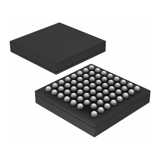
BU7963GUW
●Description
BU7963GUW is a differential serial interface connecting mobile phone LCD modules to the host CPU. Unique technology is
utilized for lower power consumption and EMI. MSDL minimizes the number of wires required - an important consideration
in hinge phones - resulting in greater reliability and design flexibility.
●Features
1) MSDL3 high-speed differential interface with a maximum transfer rate of 1350 Mbps.
2) Compatible with24-bit RGB video mode for LCD controller-to-LCD interface.
3) Pixel clock frequency range from 4 to 45MHz.
4) Depending on the data transfer rate, one, two or three differential data channels can be selected.
●Applications
Serial Interface for LCD Display Interface of Mobile Devices Application.
●Absolute Maximum Ratings:
Parameter
Power Supply Voltage
Input Voltage
Output Voltage
Input Current
Output Current
Preservation Temperature
●Operating Conditions:
Parameter
Supply Voltage for DVDD
Supply Voltage for MSVDD
Data Transmission Rate
Operating Temperature Range
www.rohm.com
© 2010 ROHM Co., Ltd. All rights reserved.
Symbol
Ratings
DVDD
-0.3 ~ +2.5
MSVDD
-0.3 ~ +2.5
-0.3 ~ MSVDD+0.3
VIN
-0.3 ~ DVDD+0.3
-0.3 ~ MSVDD+0.3
VOUT
-0.3 ~ DVDD+0.3
IIN
-10 ~ +10
IOUT
-70 ~ +70
Tstg
-55 ~ +125
Ratings
Symbol
Min
Typ
V
1.65
1.80
DVDD
V
1.65
1.80
MSVDD
DR
120
-
T
-30
25
opr
1/19
Unit
V
V
V
I/O terminals of MSVDD line
V
I/O terminals of DVDD line
V
I/O terminals of MSVDD line
V
I/O terminals of DVDD line
mA
mA
℃
Unit
Max
1.95
V
V
= V
DVDD
1.95
V
450
Mbps/ch
85
℃
No.10058EAT05
Remarks
-
-
-
-
-
Conditions
MSVDD
-
-
2010.04 - Rev.A
Advertisement

Related Manuals for Rohm BU7963GUW

Summary of Contents for Rohm BU7963GUW
- Page 1 No.10058EAT05 ●Description BU7963GUW is a differential serial interface connecting mobile phone LCD modules to the host CPU. Unique technology is utilized for lower power consumption and EMI. MSDL minimizes the number of wires required - an important consideration in hinge phones - resulting in greater reliability and design flexibility.
- Page 2 Technical Note BU7963GUW ●Package View 1PIN MARK BU7963 LOT NO. 5.0±0.1 0.08 0.75±0.1 P = 0.5×7 φ 0.295±0.05 S AB 0.05 (UNIT:mm) Fig.1. Package View (VBGA063W050) www.rohm.com 2010.04 - Rev.A 2/19 © 2010 ROHM Co., Ltd. All rights reserved.
- Page 3 PD[26:0] Parity Logic Timing CLK+ PCLK PCLK Generator Control CLK- Reset Clock Generator Detection LS[1:0] POL_PCLK Control Reference DRVR Logic PLL_BW TEST[1:0] DGND MSGND Fig.2. Block Diagram www.rohm.com 2010.04 - Rev.A 3/19 © 2010 ROHM Co., Ltd. All rights reserved.
- Page 4 PD26 MSVDD MSGND MSVDD N.C. POL_ CLK+ N.C. PCLK (D0+) (CLK+) (D1+) (D2+) CLK- N.C. N.C. DRVR TEST1 (D0-) (CLK-) (D1-) (D2-) Fig.3. Pin Layout (Top View) www.rohm.com 2010.04 - Rev.A 4/19 © 2010 ROHM Co., Ltd. All rights reserved.
- Page 5 When RVS = ‘H’ : D0- Table 3. Analog Analog 1-pin Equivalent Name Width Level Functions Shutdown Schematic 10kΩ±5% register should be connected between DRVR Analog DRVR and MSGND. www.rohm.com 2010.04 - Rev.A 5/19 © 2010 ROHM Co., Ltd. All rights reserved.
- Page 6 ‘H’: sample parallel data at rising. TEST0 Test mode pin. Pull ‘L’: normal mode. Input down ‘H’: test mode. Must be ‘L.’ TEST1 MSVDD DVDD DVDD DVDD Fig.4. Equivalent Schematics www.rohm.com 2010.04 - Rev.A 6/19 © 2010 ROHM Co., Ltd. All rights reserved.
- Page 7 Pin LS is used to control the high-speed data channel count and data format. The LS pin settings (i.e., high-speed data channel count, data format) should be the same between the transmitting and receiving devices (the BU7963GUW and BU7964GUW, respectively). Table 6 shows the PCLK input frequency ranges and transmission data rate ranges for the LS pin settings.
- Page 8 (default) PLL Bandwidth Selection BU7963GUW controls the range of the CLK+ / CLK− input frequency (= PCLK output frequency) by the setting of the data format (LS1, and LS0) of the high-speed data channel and the bandwidth setting of PLL_BW.
- Page 9 BU7963GUW goes to Standby Mode when XSD = ‘H’ and PCLK is not provided. All high-speed signaling channel outputs keep Hi-Z status. BU7963GUW is monitoring whether PCLK input is running or not and the link switches to Active Mode when PCLK running is detected.
- Page 10 ・When the number of ‘H’ bits in parallel data is even, CP bit is ‘H.’ ・When the number of ‘H’ bits in parallel data is odd, CP bits is ‘L.’ www.rohm.com 2010.04 - Rev.A 10/19 © 2010 ROHM Co., Ltd. All rights reserved.
- Page 11 DVDD = MSVDD PCLK=45MHz,XSD=‘H’ Active Current 25.4 32.9 CL=10pF op_act_rx3 3-channel/ 27-bit Format Total operating current (IDVDD + IMSVDD) with PD[26:0] inputs to ggling 0x2AAAAAA and 0x5555555 www.rohm.com 2010.04 - Rev.A 11/19 © 2010 ROHM Co., Ltd. All rights reserved.
- Page 12 PCLK Frequency≦30MHz TX_R1 Input Signal Rise Time 2 PCLK Frequency>30MHz TX_R2 Input Signal Fall Time 1 PCLK Frequency≦30MHz TX_F1 Input Signal Fall Time 2 PCLK Frequency>30MHz TX_F2 www.rohm.com 2010.04 - Rev.A 12/19 © 2010 ROHM Co., Ltd. All rights reserved.
- Page 13 Technical Note BU7963GUW 3) Serial Data Input Timing Fig.11 and Table 14 shows Serial Data Input Timing of BU7963GUW. 1.0000 ×UI CLK +/ - tTXO _N tTXO _N tTXO _ N tTXO _N D 0+/ - UI = (1 cycle time of CLK +/ - ) / 30 N = Bit position (0 ≦...
- Page 14 Unit Conditions Core power supply startup time TX_VDD_IOV Reset Valid After Power Supplied µs TX_VDD_XSD PCLK clock input startup time µs TX_IN_VAL MSDL3 output delay time TX_OUT_VAL www.rohm.com 2010.04 - Rev.A 14/19 © 2010 ROHM Co., Ltd. All rights reserved.
- Page 15 Technical Note BU7963GUW Power-Off Sequence Fig.13 shows the power-off sequence of BU7963GUW. Provided PCLK of Tx Stopped TX_ OUT_ INV Tx MSDL 3 Output Valid RX_ OUT_ INV Valid Outputs Rx All Outputs Initial Value XSD of Tx DVDD, MSVDD of Tx...
- Page 16 Technical Note BU7963GUW Frequency Change Sequence Fig.14 shows the frequency change sequence of BU7963GUW. DVDD, MSVDD of Tx and Rx TX_XSD_OUT TX_IN_XSD XSD of Tx PCLK of Tx Frequency1 Frequency2 TX_XSD_CTL TX_CTL_XSD PLL_BW of Tx State1 State2 XSD of Rx...
- Page 17 Logical input MSGND MSVDD VO - MSDL 3 TX LEAK_ TX LEAK_ RX Link detection PULL_ RX comparator output LINK_RX MSGND MSGND MSGND Fig.16. high-speed channel equivalent schematic. www.rohm.com 2010.04 - Rev.A 17/19 © 2010 ROHM Co., Ltd. All rights reserved.
- Page 18 ・ The PCB wiring for high-speed channel must not use the through-hole. ・ Do not bend the wiring for high-speed channel squarely. ・ Make the wiring length of each high-speed channel the same length (within 0.5mm). www.rohm.com 2010.04 - Rev.A 18/19 © 2010 ROHM Co., Ltd. All rights reserved.
- Page 19 0.08 S P=0.5×7 0.75±0.1 63- φ 0.295±0.05 φ 0.05 Direction of feed 1pin Reel ∗ (Unit : mm) Order quantity needs to be multiple of the minimum quantity. www.rohm.com 2010.04 - Rev.A 19/19 © 2010 ROHM Co., Ltd. All rights reserved.
- Page 20 ROHM shall bear no responsibility in any way for use of any of the Products for the above special purposes. If a Product is intended to be used for any such special purpose, please contact a ROHM sales representative before purchasing.
Need help?
Do you have a question about the BU7963GUW and is the answer not in the manual?
Questions and answers