Table of Contents
Advertisement
Quick Links
SERVICE MANUAL
Ver. 1.1 2005.07
AUDIO POWER SPECIFICATIONS (US model)
POWER OUTPUT AND TOTAL HARMONIC DISTORTION
With 8-ohm loads, both channels driven from 100 – 10,000 Hz; rated
1.0 W per channel minimum RMS power, with no more than 10% total
harmonic distortion in AC operation.
CD player section
System:
Compact disc digital audio system
Laser diode properties:
Material: GaAlAs
Wavelength: 780 nm
Emission duration: Continuous
Laser output: Less than 44.6 µW
(This output is the value measured at a distance of
about 200 mm from the objective lens surface on
the optical pick-up block with 7 mm aperture.)
Frequency response:
+1
20 – 20,000 Hz
dB
–1.5
Wow and flutter:
Below measurable limit
Radio section
Frequency range:
FM: 87.5 – 108 MHz
AM: 530 – 1,710 kHz
Sony Corporation
9-879-522-02
2005G04-1
Personal Audio Group
© 2005.07
Published by Sony Engineering Corporation
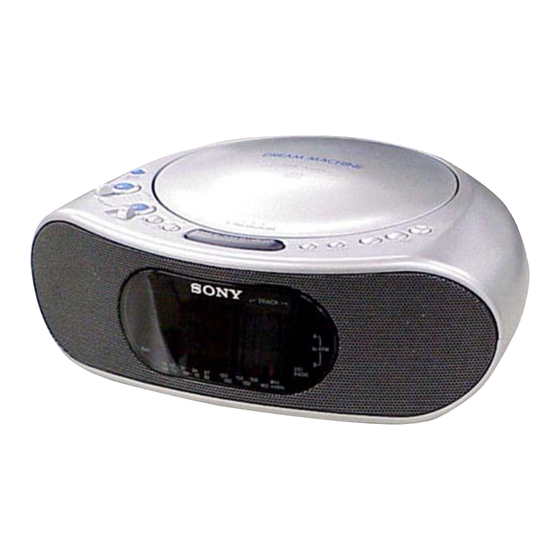
ICF-CD837
Model Name Using Similar Mechanism
CD
CD Mechanism Type
Section
Optical Pick-up Name
SPECIFICATIONS
General
Time display:
12-hour system
Speaker:
66 mm (2
inches) dia., 8 Ω
5 ⁄8
Power outputs:
1 W + 1 W (at 10% harmonic distortion)
Power requirements:
120 V AC, 60 Hz (Except Australian model)
230 V AC, 50 Hz (Australian model)
Dimensions:
Approx. 246 × 96 × 210 mm (w/h/d)
(Approx. 9
× 3
3/4
projecting parts and controls
Mass:
Approx. 1,750 g (3 lb. 86 oz.)
Design and specifications are subject to change without
notice.
FM/AM CD CLOCK RADIO
US Model
Canadian Model
E Model
Australian Model
ICF-CD832
KSM-213CDP
KSS-213C
× 8
inches) incl.
7/8
3 ⁄8
1
Advertisement
Table of Contents

Related Manuals for Sony ICF-CD837


Summary of Contents for Sony ICF-CD837
- Page 1 Radio section Frequency range: Design and specifications are subject to change without FM: 87.5 – 108 MHz notice. AM: 530 – 1,710 kHz FM/AM CD CLOCK RADIO Sony Corporation 9-879-522-02 2005G04-1 Personal Audio Group © 2005.07 Published by Sony Engineering Corporation...
- Page 2 REPLACE THESE COMPONENTS WITH SONY PARTS WHOSE NE REMPLACER CES COMPOSANTS QUE PAR DES PIÈCES PART NUMBERS APPEAR AS SHOWN IN THIS MANUAL OR SONY DONT LES NUMÉROS SONT DONNÉS DANS CE MANUEL IN SUPPLEMENTS PUBLISHED BY SONY. OU DANS LES SUPPLÉMENTS PUBLIÉS PAR SONY.
-
Page 3: Table Of Contents
ICF-CD837 • UNLEADED SOLDER TABLE OF CONTENTS Boards requiring use of unleaded solder are printed with the lead- free mark (LF) indicating the solder contains no lead. 1. SERVICING NOTES (Caution: Some printed circuit boards may not come printed with 1-1. -
Page 4: Servicing Notes
ICF-CD837 SECTION 1 SERVICING NOTES LASER DIODE AND FOCUS SEARCH OPERATION CHUCK PLATE JIG ON REPAIRING CHECK 1. Turn ON the [POWER] button and press [CD] button to CD On repairing CD section, playing a disc without the lid (CD), use position. -
Page 5: Cord Dressing (Power Cord)
ICF-CD837 1-1. CORD DRESSING (POWER CORD) 1) Set the power cord as shown in the figure. power cord 1-2. POINTER ALIGNMENT 1 Turn this in the arrow direction until stopped. MAIN board section 3 Align the notch on the boss of the knob (tune) with the direction of CV1. -
Page 6: General
ICF-CD837 SECTION 2 GENERAL This section is extracted from instruction manual. ALARM SET A ALARM SET B ALARM MODE selector The CD button has a tactile dot. AC power cord FM wire antenna VOLUME BAND TUNING There is a tactile dot... -
Page 7: Disassembly
ICF-CD837 SECTION 3 DISASSEMBLY • The equipment can be removed using the following procedure. 3-1. CABINET (UPPER) ASSY (Page 8) 3-2. FRONT PANEL ASSY 3-9. LID (CD) (Page 8) (Page 12) 3-3. POWER BOARD 3-10. LED HOLDER ASSY (Page 9) (Page 12) 3-4. -
Page 8: Cabinet (Upper) Assy
ICF-CD837 Note : Follow the disassembly procedure in the numerical order given. 3-1. CABINET (UPPER) ASSY 5 cabinet (upper) assy 4 CNP602 2 two screws ((+) BV tapping (B3)) 1 four screws ((+) BV tapping (B3)) 3-2. FRONT PANEL ASSY... -
Page 9: Power Board
ICF-CD837 3-3. POWER BOARD 3 two screws ((+) BV tapping (B3)) 4 bracket (trans) 5 POWER board 2 CNP303 1 CNP901 3-4. MAIN BOARD SECTION 1) Set the FM wire antenna as shown in the figure. 3 four screws 1 two screws... -
Page 10: Main Board, Cd Block Assy
ICF-CD837 3-5. MAIN BOARD, CD BLOCK ASSY 3 CD block assy 2 CNP703 4 MAIN board 1 three screws ((+) BV tapping (B3)) 3-6. CD MECHANISM DECK 3 chassis 4 CD cover 5 CD mechanism deck 2 two screws 1 two screws ((+) PWH tapping (B2.6)) -
Page 11: Cd Board
ICF-CD837 Ver. 1.1 3-7. CD BOARD 3 Remove the two solders of motor. 4 CNP701 5 CD board 2 Remove the two solders of motor. 1 screw (+BVTT 2 × 6 (S)) 3-8. OPTICAL PICK-UP 5 optical pick-up 1 gear (A) -
Page 12: Lid (Cd)
ICF-CD837 3-9. LID (CD) 5 lid (CD) spring (CD) 4 boss 2 boss 3 boss 1 boss 3-10. LED HOLDER ASSY 1 two screws ((+) BV tapping (B3)) 2 two screws ((+) BV tapping (B3)) 3 LED holder assy panel (front) sub assy... -
Page 13: Led Indicator Element Unit
ICF-CD837 3-11. LED INDICATOR ELEMENT UNIT DRIVE board 1 CNP502 2 Remove the solder. 3 LED indicator element unit 3-12. INDICATOR BOARD, DRIVE BOARD 5 DRIVE board 1 two screws ((+) BV tapping (B2.6)) 4 claw 3 claw 2 INDICATOR board... -
Page 14: Electrical Adjustments
ICF-CD837 SECTION 4 ELECTRICAL ADJUSTMENTS TUNER SECTION 0 dB = 1 µV AM IF ADJUSTMENT • AM Section Adjust for a maximum reading on level meter. Setting: BAND switch: AM 455 kHz VOLUME control: MIN AM RF signal AM FREQUENCY COVERAGE ADJUSTMENT... -
Page 15: Cd Section
ICF-CD837 Adjustment Location: – MAIN BOARD – ANT1 FM LEAD WIRE ANTENNA T1:AM IF ADJUSTMENT CT3,L5: FM FREQUENCY COVERAGE ADJUSTMENT CT2 CT3 CT1,L1: CT1 CT4 AM TRACKING TUNING ADJUSTMENT IC401 CT2,L2: FM TRACKING ADJUSTMENT CT4,L4: AM FREQUENCY COVERAGE ADJUSTMENT CD SECTION CD section adjustments are done automatically in this set. - Page 16 ICF-CD837 MEMO...
-
Page 17: Diagrams
ICF-CD837 SECTION 5 DIAGRAMS 5-1. BLOCK DIAGRAM — CD SECTION — LCHO CD- L INTERPOLATION SLICE ERROR MUTE DIGITAL FIN2 EFMIN MAIN LEVEL CORRECTION & FILTER SECTION CONTROL AUDIO CD ATTENUATION & RCHO CD-R (Page 18) DEEMPHASIS 1-bit DAC PH/BH... -
Page 18: Block Diagram - Main Section
ICF-CD837 5-2. BLOCK DIAGRAM — MAIN SECTION — BAND CD-L CD SECTION CV1-4 (Page 17) CD-R R-CH VREG AM OSC LPF2 CT1 CV1-1 IC301 FM/AM FRONTEND POWER AMP Q102 VR301 IF AMP,DET VOLUME ST/MO FERRITE-ROD AMRF IN MIX AMP FM/AM... -
Page 19: Circuit Boards Location
ICF-CD837 • NOTE FOR PRINTED WIRING BOARDS AND SCHEMATIC DIAGRAMS 5-3. CIRCUIT BOARDS LOCATION THIS NOTE IS COMMON FOR PRINTED WIRING BOARDS AND SCHEMATIC DIAGRAMS. (In addition to this, the necessary note is printed in each block.) BRIGHTNESS board for schematic diagram: for printed wiring boards: •... -
Page 20: Printed Wiring Board - Cd Section
ICF-CD837 5-4. PRINTED WIRING BOARD — CD SECTION — • Refer to page 19 for Circuit Boards Location. : Uses unleaded solder. (Page 22) ICF-CD837... -
Page 21: Schematic Diagram - Cd Section
ICF-CD837 5-5. SCHEMATIC DIAGRAM — CD SECTION — • Refer to page 19 for Waveforms. • Refer to page 29 for IC Block Diagrams. C727 C726 C724 C725 C721 R717 C730 C720 R716 R728 R727 C722 R718 (Page 23) C723... -
Page 22: Printed Wiring Boards - Main Section
ICF-CD837 5-6. PRINTED WIRING BOARDS — MAIN SECTION — • Refer to page 19 for Circuit Boards Location. : Uses unleaded solder. MAIN BOARD • Semiconductor Location ANT1 (ANTENNA) Ref. No. Location D301 C111 C301 R301 D401 Q102 Q101 D402... -
Page 23: Schematic Diagram - Main Section
ICF-CD837 5-7. SCHEMATIC DIAGRAM — MAIN SECTION — • Refer to page 19 for Waveforms. • Refer to page 31 for IC Pin Description of IC401. • Refer to page 30 for IC Block Diagrams. RV601 C470 R660 S651 R657... -
Page 24: Printed Wiring Boards - Display Section
ICF-CD837 5-8. PRINTED WIRING BOARDS — DISPLAY SECTION — • Refer to page 19 for Circuit Boards Location. : Uses unleaded solder. DRIVE BOARD (Page 25) KEY BOARD LED501 CNP602 LED INDICATPR UNIT CNP501 18P JW501 CNP502 CNP601 JW502 R523... -
Page 25: Printed Wiring Board - Key Section
ICF-CD837 5-9. PRINTED WIRING BOARD — KEY SECTION — • Refer to page 19 for Circuit Boards Location. : Uses unleaded solder. S653 CLOCK S653 SET/ TRACK R614 R615 S612 S612 ALARM MODE A R640 R638 R641 R639 R636 R634... -
Page 26: Schematic Diagram - Display Section
ICF-CD837 5-10. SCHEMATIC DIAGRAM — DISPLAY SECTION — Q681 Q682 Q515 R524 R523 C681 R681 C682 R682 Q517 D681 D682 R521 R522 Q514 R520 R516 Q516 CNP503 R519 R518 R517 LED501 CNP502 CNP501 R515 R514 S612 R641 R640 R513 R512... -
Page 27: Printed Wiring Board - Power Supply Section
ICF-CD837 5-11. PRINTED WIRING BOARD — POWER SUPPLY SECTION — • Refer to page 19 for Circuit Boards Location. : Uses unleaded solder. POWER BOARD W302 SP101 (Page 22) SPEAKER MAIN BOARD (L-CH) CNP901 SP201 SPEAKER (R-CH) L902 CNP302 BH901... -
Page 28: Schematic Diagram - Power Supply Section
ICF-CD837 Ver. 1.1 5-12. SCHEMATIC DIAGRAM — POWER SUPPLY SECTION — R307 C221 BH303 R216 R218 C219 C220 R213 C218 R219 Q204 TP204 W302 CNP302 R214 SP201 R220 TP205 Q301 R215 D302 TP302 (Page 23) TP206 C216 TP106 R303 TP105... - Page 29 ICF-CD837 • IC Block Diagrams IC701 LC78646E-US-E (CD Board) 78 77 76 75 74 73 72 71 69 68 67 66 65 64 63 62 61 FIN1 – FIN2 – TIN1 TBAL – – TIN2 – – TBAL – RFMON...
- Page 30 ICF-CD837 IC702 BA5826FP-E2 (CD Board) IC301 LA4627 (POWER Board) SP– D.BUFF SL– D.BUFF LEVEL D.BUFF SHIFT – D.BUFF SPIN LEVEL SHIFT – SLIN FILTER THERMAL SHUT-DOWN MONITOR (SLIN) REG–B VREF REGO MUTE (FIN) DRIVER MUTE (TIN) LEVEL LEVEL SHIFT D.BUFF SHIFT D.BUFF...
- Page 31 ICF-CD837 • IC Pin Description IC401 uPD789477GC-A28-8BT (SYSTEM CONTROL) Pin No. Pin Name Pin Description 1 to 29 — Note used (Open) 30 to 37 SEG7 to SEG0 LED segment driver signal output AVDD — Power supply pin (+3.3 V)
-
Page 32: Exploded Views
ICF-CD837 Ver. 1.1 SECTION 6 EXPLODED VIEWS NOTE: • The mechanical parts with no reference • Color Indication of Appearance Parts The components identified by mark 0 or dotted line with mark number in the exploded views are not supplied. -
Page 33: Front Panel Section
ICF-CD837 Ver. 1.1 6-2. FRONT PANEL SECTION SP101 CNP501 LED501 not supplied SP201 Ref. No. Part No. Description Remark Ref. No. Part No. Description Remark A-1094-529-A DRIVE BOARD, COMPLETE 1-830-248-11 CABLE, FLEXIBLE FLAT (18 CORE) 3-254-151-01 SCREW (B2.6), (+) P TAPPING... -
Page 34: Upper Cabinet Section
ICF-CD837 Ver. 1.1 6-3. UPPER CABINET SECTION S401 Ref. No. Part No. Description Remark Ref. No. Part No. Description Remark 2-541-550-01 LID (CD) (WHITE)...(WHITE) (Print color:BLUE) 2-541-541-01 BUTTON (ALARM A) (BLUE)...(WHITE/BLACK) 2-541-550-11 LID (CD) (BLACK)...(BLACK) 2-541-541-11 BUTTON (ALARM A) (PINK)...(WHITE) 2-541-550-51 LID (CD) (WHITE)...(WHITE) (Print color:PINK) -
Page 35: Lower Cabinet Section
ICF-CD837 Ver. 1.1 6-4. LOWER CABINET SECTION not supplied T901 ANT1 F901 The components identified by Les composants identifiés par une mark 0 or dotted line with mark marque 0 sont critiques pour 0 are critical for safety. la sécurité. -
Page 36: Cd Block Section
ICF-CD837 Ver. 1.1 6-5. CD BLOCK SECTION Ref. No. Part No. Description Remark Ref. No. Part No. Description Remark 3-923-736-01 COVER, CD A-4542-980-A CD BOARD, COMPLETE 3-046-853-11 RUBBER, VIBRATION PROOF (GREEN) 3-046-853-01 RUBBER, VIBRATION PROOF (RED) 3-252-828-01 SCREW (B2.6), (+) PWH TAPPING... -
Page 37: Cd Mechanism Section
ICF-CD837 6-6. CD MECHANISM SECTION (KSM-213CDP) not supplied not supplied (M701 (SPINDLE)) M702 The components identified by Les composants identifiés par une mark 0 or dotted line with mark marque 0 sont critiques pour 0 are critical for safety. la sécurité. -
Page 38: Electrical Parts List
ICF-CD837 Ver. 1.1 SECTION 7 BRIGHTNESS ELECTRICAL PARTS LIST NOTE: • Due to standardization, replacements in • SEMICONDUCTORS The components identified by mark 0 or dotted line with mark the parts list may be different from the In each case, u : µ, for example: 0 are critical for safety. - Page 39 ICF-CD837 DRIVE Ref. No. Part No. Description Remark Ref. No. Part No. Description Remark < TRANSISTOR > A-1094-529-A DRIVE BOARD, COMPLETE ********************** Q701 8-729-054-57 TRANSISTOR KTN2907AS-RTK < CONNECTOR > < RESISTOR > CNP502 1-779-286-11 CONNECTOR, FFC (LIF(NON-ZIF)) 18P R701 1-216-841-11 METAL CHIP...
- Page 40 ICF-CD837 Ver. 1.1 INDICATOR MAIN Ref. No. Part No. Description Remark Ref. No. Part No. Description Remark A-1094-532-A INDICATOR BOARD, COMPLETE R639 1-216-837-11 METAL CHIP 1/10W R640 1-216-837-11 METAL CHIP 1/10W ************************** R641 1-216-837-11 METAL CHIP 1/10W < CAPACITOR >...
- Page 41 ICF-CD837 MAIN Ref. No. Part No. Description Remark Ref. No. Part No. Description Remark 1-164-315-11 CERAMIC CHIP 470PF C439 1-162-970-11 CERAMIC CHIP 0.01uF C103 1-162-970-11 CERAMIC CHIP 0.01uF C440 1-162-919-11 CERAMIC CHIP 22PF C104 1-162-970-11 CERAMIC CHIP 0.01uF C441 1-162-919-11 CERAMIC CHIP...
- Page 42 ICF-CD837 MAIN Ref. No. Part No. Description Remark Ref. No. Part No. Description Remark D401 8-719-911-19 DIODE 1SS119-25 R102 1-216-829-11 METAL CHIP 4.7K 1/10W D402 8-719-911-19 DIODE 1SS119-25 R103 1-216-829-11 METAL CHIP 4.7K 1/10W D403 8-719-063-79 DIODE 1N4002B R104 1-216-845-11 METAL CHIP...
- Page 43 ICF-CD837 Ver. 1.1 MAIN POWER Ref. No. Part No. Description Remark Ref. No. Part No. Description Remark R433 1-216-809-11 METAL CHIP 1/10W < VIBRATOR > R434 1-216-809-11 METAL CHIP 1/10W R435 1-216-821-11 METAL CHIP 1/10W X401 1-760-252-12 VIBRATOR, CRYSTAL (32kHz)
- Page 44 ICF-CD837 Ver. 1.1 POWER Ref. No. Part No. Description Remark Ref. No. Part No. Description Remark L902 1-410-513-11 INDUCTOR 22uH MISCELLANEOUS *************** < TRANSISTOR > 1-830-248-11 CABLE, FLEXIBLE FLAT (18 CORE) Q104 6-550-364-01 TRANSISTOR 2SD2652T106 1-830-247-11 CABLE, FLEXIBLE FLAT (6 CORE)
- Page 45 ICF-CD837 MEMO...
- Page 46 ICF-CD837 REVISION HISTORY Clicking the version allows you to jump to the revised page. Also, clicking the version at the upper on the revised page allows you to jump to the next revised page. Ver. Date Description of Revision 2005.02 2005.07...
Need help?
Do you have a question about the ICF-CD837 and is the answer not in the manual?
Questions and answers