Table of Contents
Advertisement
Quick Links
Freescale Semiconductor
Data Sheet: Advance Information
An Energy-Efficient Solution by Freescale
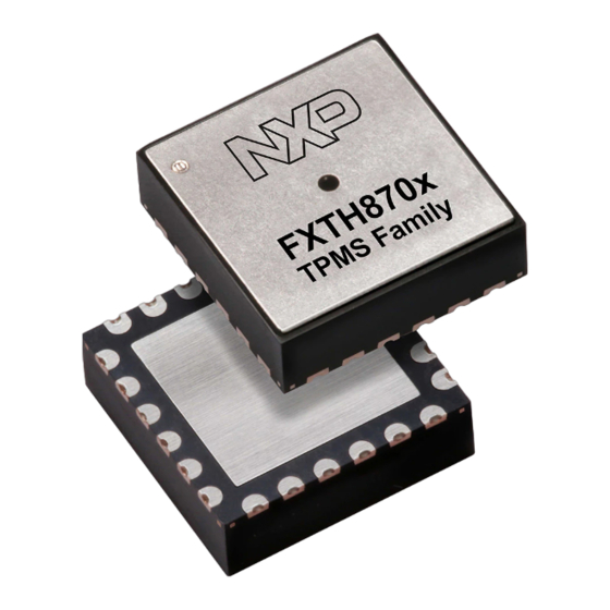
FXTH870xD Tire Pressure Monitor
Sensor
The FXTH870xD family is comprised of the following functions all within the
same package.
Features
•
Pressure sensor with one of two calibrated pressure ranges
— 100 - 450 kPa
— 100 - 900 kPa
•
Temperature sensor
•
Optional XZ- or Z-axis accelerometer with adjustable offset option
•
Voltage reference measured by ADC10
•
Six-channel, 10-bit analog-to-digital converter (ADC10) with two external
I/O inputs
•
8-bit MCU
— S08 Core with SIM and interrupt
— 512 RAM
— 8K FLASH (in addition to 8K providing factory firmware and trim
data)
— 64-byte, low-power, parameter registers
•
Dedicated state machines to sequence routine measurement and
transmission processes for reduced power consumption
•
Internal 315-/434-MHz RF transmitter
— External crystal oscillator
— PLL-based output with fractional-n divider
— OOK and FSK modulation capability
— Programmable data rate generator
— Manchester, Bi-Phase or NRZ data encoding
— 256-bit RF data buffer variable length interrupt
— Direct access to RF transmitter from MCU for unique formats
— Low power consumption (less than 8 mA at 434 MHz, 5 dBM at
3.0 V, 25 °C)
•
Differential input LF detector/decoder on independent signal pins
•
Seven multipurpose GPIO pins
— Four pins can be connected to optional internal pullups/pulldowns and STOP4 wakeup interrupt
— Two of seven pins can be connected to a channel on the ADC10
— Two of seven pins can be connected to a channel on the TPM1
•
Real-Time Interrupt driven by LFO with interrupt intervals of
8, 16, 32, 64, 128, 256, 512 or 1024 ms
•
Low-power, wakeup timer and periodic reset driven by LFO
•
Watchdog timeout with selectable times and clock sources
•
Two-channel general purpose timer/PWM module (TPM1)
This document contains information on a new product. Specifications and information herein
are subject to change without notice.
© 2014-2015 Freescale Semiconductor, Inc. All rights reserved.
Document Number: FXTH870xD
Rev. 1.4, 02/2015
FXTH870xD
Top and bottom view
24-Pin, 1-hole lid
7 x 7 QFN
Top view
ID Feature
on top lid
PTB1
1
PTA2
2
PTA1
3
PTA0
4
RESET
5
V
6
SS
Pin connections
18 PTA3
17
LFA
16
LFB
15
BKGD/PTA4
14
X0
13
X1
Advertisement
Table of Contents

Related Manuals for NXP Semiconductors FXTH870 D Series


Summary of Contents for NXP Semiconductors FXTH870 D Series
- Page 1 Freescale Semiconductor Document Number: FXTH870xD Data Sheet: Advance Information Rev. 1.4, 02/2015 An Energy-Efficient Solution by Freescale FXTH870xD Tire Pressure Monitor Sensor FXTH870xD The FXTH870xD family is comprised of the following functions all within the same package. Features Top and bottom view •...
- Page 2 • Internal oscillators — MCU bus clock of 0.5, 1, 2 and 4 MHz (1, 2, 4 and 8 MHz HFO) — Low frequency, low power time clock (LFO) with 1 ms period — Medium frequency, controller clock (MFO) of 8 sec period •...
-
Page 3: Table Of Contents
Contents General Information ................4 Overall Block Diagram . - Page 4 Timer Pulse-Width Module............... . 68 Features .
- Page 5 14 Firmware ..................133 14.1 Software Jump Table .
-
Page 6: General Information
General Information Overall Block Diagram The block diagram of the FXTH870xD is shown in Figure 1. This diagram covers all the main blocks mentioned above and their main signal interactions. Power management controls and bus control signals are not shown in this block diagram for clarity. Multi-Chip Interface The FXTH870xD contains two to three devices using the best process technology for each. - Page 7 TRANSDUCERS PRESS TIMER SENSOR 1 ms ACCEL ACCEL TIMER (OPTION) (OPTION) BKGD SENS PTA4 MCU CORE TEMP ADC10 RESTART 10-BIT TEMP TEMP SENSOR 6-CHAN 64 Byte PARAMETER 1, 2, 4 or 8 REGISTER BANDGAP 8 Sec MEMORY 8K USER FLASH RESET MEMORY VOLT...
-
Page 8: Reference Documents
SYSTEM ADC10 CONTROL RTICLKS CLOCK LOGIC 1 mS PERIOD ADC10 FLASH BUSCLKS[1:0] ADCCLK ADC10 HFO OSC 4 kbps 2 1, 2, 4, and 8 MHz CLSA, CLKSB COPCLKS (125 kHz) WATCH LFRO TPM1 OSCILL (1 kHz) RANDOM PTA3 (0 - 1 MHz) TCLKDIV (500 kHz) (1 kHz) -
Page 9: Pins And Connections
Pins and Connections This section describes the pin layout and general function of each pin. Package Pinout The pinout for the FXTH870xD device QFN package is shown in Figure 3 for the orientation of the pressure port up. The orientation of the internal Z-axis accelerometer is shown in Figure Top View ID Feature... -
Page 10: Signal Properties
Signal Properties The following sections describe the general function of each pin. L1 and matching network optimized for specific PWB and antenna layout. Recommend R2 and R3, <10 k 0603 minimum size for L1 and recommended for other matching network inductors highest EMC resistance BKGD/PTA4 for maximum efficiency. - Page 11 Care should be taken to reduce measurement signal noise by separating the V , AV , AV and RV pins using a “star” connection such that each metal trace does not share any load currents with other external devices as shown in Figure Bypass capacitors FXTH870xxx and Other Load Currents...
- Page 12 2.3.9 PTA[3:2] Pins The PTA[3:2] pins are general purpose I/O pin. These two pins can be configured as normal bidirectional I/O pin with programmable pullup or pulldown devices and/or wakeup interrupt capability; or one or both can be connected to the two input channels of the Timer Pulse Width (TPM1) module.
-
Page 13: Modes Of Operation
Modes of Operation The operating modes of the FXTH870xD are described in this section. Entry into each mode, exit from each mode, and functionality while in each of the modes are described. Features • ACTIVE BACKGROUND DEBUG mode for code development •... -
Page 14: Stop Modes
STOP Modes One of two stop modes are entered upon execution of a STOP instruction when the STOPE bit in the system option register is set. In all STOP modes, all internal clocks are halted except for the low frequency 1 kHz oscillator (LFO) which runs continuously whenever power is applied to the V and V pins. - Page 15 Table 1. STOP Mode Behavior (continued) Mode STOP1 STOP4 Regulator I/O Pins Hi-Z States Held Wakeup Methods Interrupts, resets Interrupts, resets 1. RTI can be used in STOP1 or STOP4 if the clock selected is the LFO. To use the HFO as the clock the MCU must be in the RUN mode. 2.
- Page 16 ADC10 The internal asynchronous ADC10 clock is always used as the conversion clock. The ADC10 can continue operation during STOP4 mode. Conversions can be initiated while the MCU is the STOP4 mode. All ADC10 module registers contain their reset values following exit from STOP1 mode. When the MCU enters STOP mode the detectors in the LFR will remain powered up depending on the states of the bits selecting the periodic sampling.
-
Page 17: Memory
Memory The overall memory map of the FXTH870xD resides on the MCU. MCU Memory Map As shown in Figure 8, MCU on-chip memory in the FXTH870xD consists of parameter registers, RAM, FLASH program memory for nonvolatile data storage, and I/O and control/status registers. The registers are divided into four groups: •... -
Page 18: Mcu Register Addresses And Bit Assignments
Table 2. Vector Summary (continued) User Vector Addr Vector Name Module Source $DFEE:DFEF $DFF0:DFF1 Vtpm1ovf TPM1 $DFF2:DFF3 Vtpm1ch1 TPM1 $DFF4:DFF5 Vtpm1ch0 TPM1 $DFF6:DFF7 Vwuktmr $DFF8:DFF9 Vlvd Sys Ctrl - LVD $DFFA:DFFB Reserved $DFFC:DFFD Vswi SWI opcode Sys Ctrl - POR, PRF, COP, LVD $DFFE:DFFF Vreset Temp Restart, Illegal opcode or address... - Page 19 Table 3. MCU Direct Page Register Summary (continued) Address Register Name Bit 7 Bit 0 $000D KBIPE KBIPE[3:0] $000E KBIES KBEDG[3:0] $000F Reserved $0010 TPM1SC TOIE CPWMS CLKSB CLKSA $0011 TPM1CNTH Bit [15:8] $0012 TPM1CNTL Bit [7:0] $0013 TPM1MODH Bit [15:8] $0014 TPM1MODL Bit [7:0]...
- Page 20 Table 5. LFR Register Summary - LPAGE = 1 Address Register Name Bit 7 Bit 0 $0020 LFCTL1 LFEN SRES CARMOD LPAGE IDSEL[1:0] SENS[1:0] $0021 LFCTRLE TRIMEE AZSC[2:0] $0022 LFCTRLD AVFOF[1:0} DEQS AZDC[1:0] ONMODE CHK125[1:0] $0023 LFCTRLC AMPGAIN[1:0] FINSEL[1:0] AZEN LOWQ[1:0] DEQEN $0024...
- Page 21 Table 7. RFM Register Summary - RPAGE = 1 Address Register Name Bit 7 Bit 0 $0030 RFCR0 BPS[7:0] $0031 RFCR1 FRM[7:0] $0032 RFCR2 SEND RPAGE PWR[4:0] $0033 RFCR3 DATA IFPD ISPC IFID FNUM[3:0] $0034 RFCR4 RFBT[7:0] $0035 RFCR5 BOOST LFSR[6:0] $0036 RFCR6...
-
Page 22: High Address Registers
High Address Registers High-page registers are used much less often, so they are located above $1800 in the memory map. This leaves more room in the direct page for more frequently used registers and variables. The registers control system level features as given in Table Table 8. -
Page 23: Flash
None of the RAM locations are used directly by the firmware provided by Freescale. The firmware routines utilize RAM only through stack operations; and the user needs to be aware of stack depth required by each routine as described in the CodeWarrior project files supplied by Freescale. - Page 24 Write the command code for the desired command to FCMD. The five valid commands are blank check (0x05), byte program (0x20), burst program (0x25), page erase (0x40), and mass erase (0x41). The command code is latched into the command buffer. Write a 1 to the FCBEF bit in FSTAT to clear FCBEF and launch the command (including its address and data information).
- Page 25 Note 1: Required only once after reset. WRITE TO FCDIV FLASH PROGRAM AND START ERASE FLOW FACCERR? CLEAR ERROR WRITE TO FLASH TO BUFFER ADDRESS AND DATA WRITE COMMAND TO FCMD WRITE 1 TO FCBEF Note 2: Wait at least four bus cycles before checking FCBEF or FCCF.
- Page 26 Note 1: Required only once after reset. WRITE TO FCDIV FLASH BURST START PROGRAM FLOW FACCERR? CLEAR ERROR FCBEF? WRITE TO FLASH TO BUFFER ADDRESS AND DATA WRITE COMMAND ($25) TO FCMD WRITE 1 TO FCBEF Note 2: Wait at least four bus cycles before TO LAUNCH COMMAND checking FCBEF or FCCF.
- Page 27 • Writing the byte program, burst program, or page erase command code (0x20, 0x25, or 0x40) with a BACKGROUND DEBUG command while the MCU is secured (the BACKGROUND DEBUG controller can only do blank check and mass erase commands when the MCU is secure.) •...
-
Page 28: Security
Security The FXTH870xD includes circuitry to prevent unauthorized access to the contents of FLASH and RAM memory. When security is engaged, FLASH and RAM are considered secure resources. Direct-page registers, high-page registers, and the BACKGROUND DEBUG controller are considered unsecured resources. Programs executing within secure memory have normal access to any MCU memory locations and resources. -
Page 29: Flash Registers And Control Bits
FLASH Registers and Control Bits The FLASH module has nine 8-bit registers in the high-page register space, three locations in the nonvolatile register space in FLASH memory which are copied into three corresponding high-page control registers at reset. There is also an 8-byte comparison key in FLASH memory. - Page 30 4.9.2 FLASH Options Register (FOPT and NVOPT) During reset, the contents of the nonvolatile location NVOPT are copied from FLASH into FOPT. Bits 5 through 2 are not used and always read 0. This register may be read at any time, but writes have no meaning or effect. To change the value in this register, erase and reprogram the NVOPT location in FLASH memory as usual and then issue a new MCU reset.
- Page 31 Table 14. FCNFG Register Field Descriptions Field Description Enable Writing of Access Key — This bit enables writing of the backdoor comparison key. For more detailed information about the backdoor key mechanism, refer to Section 4.8. 0 Writes to 0xFFB0–0xFFB7 are interpreted as the start of a FLASH programming or erase command KEYACC 1 Writes to NVBACKKEY (0xFFB0–0xFFB7) are interpreted as comparison key writes 4.9.4...
- Page 32 Table 16. FSTAT Register Field Descriptions (continued) Field Description FLASH Command Complete Flag — FCCF is set automatically when the command buffer is empty and no command is being processed. FCCF is cleared automatically when a new command is started (by writing 1 to FCBEF to register a command). Writing to FCCF has no meaning or effect.
-
Page 33: Reset, Interrupts And System Configuration
Reset, Interrupts and System Configuration This section discusses basic reset and interrupt mechanisms and the various sources of reset and interrupts in the FXTH870xD. Some interrupt sources from peripheral modules are discussed in greater detail within other sections of this product specification. This section gathers basic information about all reset and interrupt sources in one place for easy reference. -
Page 34: Sim Test Register (Simtst)
Table 18. COP Watchdog Timeout Period (continued) COPT Clock COP Overflow Time COPCLKS Overflow Source (ms, nominal) Count 2048 2048 BUSCLKS[1:0] 1:1 (0.5 MHz) 1:0 (1 MHz) 0:1 (2 MHz) 0:0 (4MHz) Bus Clock 16.384 8.192 4.096 2.048 Bus Clock 32.768 16.384 8.192... -
Page 35: Interrupts
Interrupts Interrupts provide a way to save the current CPU status and registers, execute an interrupt service routine (ISR), and then restore the CPU status so processing resumes where it left off before the interrupt. Other than the software interrupt (SWI), which is a program instruction, interrupts are caused by hardware events. - Page 36 UNSTACKING Towards LOWER Addresses ORDER SP after interrupt stacking CONDITION CODE REGISTER ACCUMULATOR INDEX REGISTER* (LOW BYTE X) PROGRAM COUNTER HIGH PROGRAM COUNTER LOW SP before the interrupt STACKING Towards HIGHER Addresses ORDER * High byte (H) of index register is not automatically stacked. Figure 19.
- Page 37 Table 20. Vector Summary Jump Table Vector Vector Vector Module Vector Addr Flags Enables Description Priority Name Source (High/Low) $DFE0 - $DFE1 Vkbi KBIE Keyboard interrupt pins PTA[3:0] $DFE2 - $DFE3 Reserved $DFE4 - $DFE5 Reserved Interrupt from the RTI when the periodic $DFE6 - $DFE7 Vrti Sys Ctrl...
-
Page 38: Low-Voltage Detect (Lvd) System
Low-Voltage Detect (LVD) System The FXTH870xD includes a system to detect low voltage conditions in order to protect memory contents and control MCU system states during supply voltage variations. The system is comprised of a power-on reset (POR) circuit and an LVD circuit with a user selectable trip voltage, either high (V ) or low (V ). -
Page 39: Real Time Interrupt
Real Time Interrupt The RTI uses the internal low frequency oscillator (LFO) as its clock source. The RTI can be used as a periodic interrupt in MCU RUN mode, or can be used as a periodic wakeup from all low power modes. The LFO is always active and cannot be powered off by any software control. -
Page 40: Temperature Sensor And Restart System
Table 24. Real-Time Interrupt Period Delay Timing (ms) RTIS2 RTIS1 RTIS0 (Dependent on 1-kHz LFO) 5.10 Temperature Sensor and Restart System The FXTH870xD has two temperature sensing mechanisms. The first is an accurate sensor which is accessible through the ADC10 channel 1. The second is a less accurate, very low power sensor which generates a wakeup from STOP1 when the temperature crosses its threshold of detection. - Page 41 Table 25. SRS Register Field Descriptions Field Description Power-On Reset — This bit indicates reset was caused by the power-on detection logic. Because the internal supply voltage was ramping up at the time, the low-voltage reset (LVR) status bit is also set to indicate that the reset occurred while the internal supply was below the LVR threshold.
- Page 42 Table 26. SIMOPT1 Register Field Descriptions (continued) Field Description COP Clock Select — This control bit selects the clock source for the COP watchdog timer. This bit is a write-once bit so that only the first write after reset is honored. This bit is cleared by an MCU reset. COPCLKS 0 Select the LFO oscillator output.
- Page 43 Table 27. SIMOPT2 Register Field Descriptions (continued) Field Description Bus Clock Select — Bus clock frequency selection by changing HFO FLL ratio as shown in Figure 2. The bus clock frequency is always the HFO frequency divided by two. These bits are cleared by a reset and can be written at any time. 00 Bus Frequency = 4 MHz (HFO = 8 MHz) BUSCLKS 01 Bus Frequency = 2 MHz (HFO = 4 MHz)
- Page 44 5.11.5 System Power Management Status and Control 2 Register (SPMSC2) This register is used to configure the STOP mode behavior of the MCU. $180A PPDACK Power-on reset: Any other reset: = Reserved U = Unaffected by reset 1. This bit can be written only one time after reset. Additional writes are ignored. Figure 25.
-
Page 45: System Stop Exit Status Register (Simses)
Table 30. SRTISC Register Field Descriptions (continued) Field Description Low-Voltage Warning Acknowledge — The LVWF bit indicates the low voltage warning status. LVWACK Writing a logic 1 to LVWACK clears LVWF to a logic 0 if a low voltage warning is not present. Low-Voltage Detect Voltage Select —... -
Page 46: General Purpose I/O
General Purpose I/O This section explains software controls related to general purpose input/output (I/O) and pin control. The FXTH870xD has seven general-purpose I/O pins which are comprised of a general use 5-bit port A and a 2-bit port B. PTA[4:0] pins are shared with on-chip peripheral functions. PTB[1:0] pins are GPIO only, and are multiplexed with the LF receiver block (see Section 6.5 for additional details regarding mutually exclusive operations).The peripheral modules have priority over... - Page 47 KBEDEy PTA[3:0] only KBIPGy PTxPEn PTxDDn Write PTxDn Read Port pin PTxDn KBEDGy PTA[3:0] only KBIPEy PTxPEn KBI interrupt KBMOD KBACK Figure 29. General Purpose I/O Logic Table 32. Truth Table for Pullup and Pulldown Resistors PTAPE[3:0] PTADD[3:0] KBIPE[3:0] KBEDG[3:0] Pullup Pulldown (pull enable)
-
Page 48: Unused Pin Configuration
An internal pullup device can be enabled for each port pin by setting the corresponding bit in one of the pullup enable registers (PTxPEn). The pullup device is disabled if the pin is configured as an output by the general purpose I/O control logic or any shared peripheral function regardless of the state of the corresponding pullup enable register bit. - Page 49 Table 33. Port A Data Register Field Descriptions Field Description Port A Data Register Bit — For port A pins that are inputs, reads return the logic level on the pin. For port A pins that are configured as outputs, reads return the last value written to this register. Writes are latched into all bits of this register.
-
Page 50: Port B Registers
Port B Registers Port B PTB[1:0] functions are multiplexed with the LF receiver block such that the port B GPIOs become high impedance when the LF block has been enabled. When the LF block is disabled, port B pins operate as described here. $0004 Bit 7 Bit 0... -
Page 51: Keyboard Interrupt
Keyboard Interrupt The FXTH870xD has a KBI module with general purpose I/O pins. Features The KBI features include: • Up to four keyboard interrupt pins with individual pin enable bits. • Each keyboard interrupt pin is programmable as falling edge (or rising edge) only, or both falling edge and low level (or both rising edge and high level) interrupt sensitivity. -
Page 52: Register Definitions
Register Definitions The KBI includes three registers: • An 4-bit pin status and control register. • An 4-bit pin enable register. • An 4-bit edge select register. 7.5.1 KBI Status and Control Register (KBISC) KBISC contains the status flag and control bits, which are used to configure the KBI. $000C KBIE KBMOD... -
Page 53: Functional Description
7.5.3 KBI Edge Select Register (KBIES) KBIES contains the edge select control bits. $000E KBEDG7 KBEDG6 KBEDG5 KBEDG4 KBEDG3 KBEDG2 KBEDG1 KBEDG0 Reset: Figure 39. KBI Edge Select Register Table 42. KBIES Register Field Descriptions Field Description Keyboard Edge Selects — Each of the KBEDGn bits selects the falling edge/low level or rising edge/high level function of the corresponding pin). -
Page 54: Central Processing Unit
Central Processing Unit Introduction This section provides summary information about the registers, addressing modes, and instruction set of the CPU of the HCS08 Family. For a more detailed discussion, refer to the HCS08 Family Reference Manual, volume 1, Freescale Semiconductor document order number HCS08RMV1/D. -
Page 55: Programmer's Model And Cpu Registers
Programmer’s Model and CPU Registers Figure 40 shows the five CPU registers. CPU registers are not part of the memory map. ACCUMULATOR 16-BIT INDEX REGISTER H:X INDEX REGISTER (HIGH INDEX REGISTER (LOW) STACK POINTER PROGRAM COUNTER CONDITION CODE REGISTER V 1 1 H I N Z CARRY ZERO NEGATIVE... - Page 56 8.3.4 Program Counter (PC) The program counter is a 16-bit register that contains the address of the next instruction or operand to be fetched. During normal program execution, the program counter automatically increments to the next sequential memory location every time an instruction or operand is fetched.
-
Page 57: Addressing Modes
Table 43. CCR Register Field Descriptions (continued) Field Description Carry/Borrow Flag — The CPU sets the carry/borrow flag when an addition operation produces a carry out of bit 7 of the accumulator or when a subtraction operation requires a borrow. Some instructions — such as bit test and branch, shift, and rotate —... -
Page 58: Special Operations
8.4.6.3 Indexed, 8-Bit Offset (IX1) This variation of indexed addressing uses the 16-bit value in the H:X index register pair plus an unsigned 8-bit offset included in the instruction as the address of the operand needed to complete the instruction. 8.4.6.4 Indexed, 8-Bit Offset with Post Increment (IX1+) This variation of indexed addressing uses the 16-bit value in the H:X index register pair plus an unsigned 8-bit offset included in... -
Page 59: Hcs08 Instruction Set Summary
certain that the interrupt service routine does not use any instructions or auto-increment addressing modes that might change the value of H. The software interrupt (SWI) instruction is like a hardware interrupt except that it is not masked by the global I bit in the CCR and it is associated with an instruction opcode within the program so it is not asynchronous to program execution. - Page 60 Index register, lower order (least significant) 8 bits Program counter Program counter, higher order (most significant) 8 bits Program counter, lower order (least significant) 8 bits Stack pointer Memory and addressing A memory location or absolute data, depending on addressing mode M:M + 0x0001 A 16-bit value in two consecutive memory locations.
- Page 61 Address modes Inherent (no operands) 8-bit or 16-bit immediate 8-bit direct 16-bit extended 16-bit indexed no offset 16-bit indexed no offset, post increment (CBEQ and MOV only) 16-bit indexed with 8-bit offset from H:X IX1+ 16-bit indexed with 8-bit offset, post increment (CBEQ only) 16-bit indexed with 16-bit offset from H:X 8-bit relative offset...
- Page 62 Table 44. HCS08 Instruction Set Summary (Sheet 2 of 8) Effect on CCR Source Operation Description Form V H I N Z C ASR opr8a ASRA ASRX Arithmetic Shift Right Þ – – Þ Þ Þ ASR oprx8,X ASR ,X ASR oprx8,SP 9E67 BCC rel...
- Page 63 Table 44. HCS08 Instruction Set Summary (Sheet 3 of 8) Effect on CCR Source Operation Description Form V H I N Z C – – – – – – BMI rel Branch if Minus Branch if (N) = 1 2B rr Branch if Interrupt Mask –...
- Page 64 Table 44. HCS08 Instruction Set Summary (Sheet 4 of 8) Effect on CCR Source Operation Description Form V H I N Z C CMP #opr8i CMP opr8a CMP opr16a hh ll (A) – (M) CMP oprx16,X Compare Accumulator ee ff (CCR Updated But Operands Not Þ...
- Page 65 Table 44. HCS08 Instruction Set Summary (Sheet 5 of 8) Effect on CCR Source Operation Description Form V H I N Z C JMP opr8a JMP opr16a hh ll PC Jump Address JMP oprx16,X Jump – – – – – – ee ff JMP oprx8,X JMP ,X...
- Page 66 Table 44. HCS08 Instruction Set Summary (Sheet 6 of 8) Effect on CCR Source Operation Description Form V H I N Z C Nibble Swap A (A[3:0]:A[7:4]) – – – – – – INH Accumulator ORA #opr8i ORA opr8a ORA opr16a hh ll ORA oprx16,X...
- Page 67 Table 44. HCS08 Instruction Set Summary (Sheet 7 of 8) Effect on CCR Source Operation Description Form V H I N Z C STA opr8a STA opr16a hh ll STA oprx16,X ee ff Store Accumulator in M (A) STA oprx8,X 0 –...
- Page 68 Table 44. HCS08 Instruction Set Summary (Sheet 8 of 8) Effect on CCR Source Operation Description Form V H I N Z C Enable Interrupts; Wait I bit 0; Halt CPU WAIT – – 0 – – – INH for Interrupt 1.
- Page 69 Table 45. Opcode Map (Sheet 2 of 2) Bit-Manipulation Branch Read-Modify-Write Control Register/Memory 9E60 6 9ED0 5 9EE0 4 9E61 6 9ED1 5 9EE1 4 CBEQ 9ED2 5 9EE2 4 9E63 6 9ED3 5 9EE3 4 9EF3 6 CPHX 9E64 6 9ED4 5 9EE4 4 9ED5 5...
-
Page 70: Timer Pulse-Width Module
Timer Pulse-Width Module The timer pulse-width module (TPM1) is a two channel timer system that supports traditional input capture, output compare, or edge-aligned PWM on each channel. All the features and functions of the TPM1 are as described in the MC9S08RC16 product specification. -
Page 71: External Signal Description
9.2.1 Block Diagram Figure 42 shows the structure of a TPM1. BUSCLK CLOCK SOURCE PRESCALE AND SELECT SELECT DIVIDE BY OFF, BUS, XCLK, EXT SYNC 1, 2, 4, 8, 16, 32, 64, or 128 CLKSB CLKSA CPWMS MAIN 16-BIT COUNTER INTERRUPT COUNTER RESET LOGIC... -
Page 72: Register Definition
Register Definition The TPM1 includes: • An 8-bit status and control register (TPMSC) • A 16-bit counter (TPMCNTH:TPMCNTL) • A 16-bit modulo register (TPMMODH:TPMMODL) Each timer channel has: • An 8-bit status and control register (TPMCnSC) • A 16-bit channel value register (TPMCnVH:TPMCnVL) 9.4.1 Timer Status and Control Register (TPM1SC) TPM1SC contains the overflow status flag and control bits that are used to configure the interrupt enable, TPM1 configuration,... - Page 73 Table 48. Prescale Divisor Selection PS2:PS1:PS0 TPM1 Clock Source Divided-By 0:0:0 0:0:1 0:1:0 0:1:1 1:0:0 1:0:1 1:1:0 1:1:1 9.4.2 Timer Counter Registers (TPM1CNTH:TPM1CNTL) The two read-only TPM1 counter registers contain the high and low bytes of the value in the TPM1 counter. Reading either byte (TPM1CNTH or TPM1CNTL) latches the contents of both bytes into a buffer where they remain latched until the other byte is read.
- Page 74 $0014 Bit 7 Bit 0 Reset Figure 47. Timer Counter Modulo Register Low (TPM1MODL) It is good practice to wait for an overflow interrupt so both bytes of the modulo register can be written well before a new overflow. An alternative approach is to reset the TPM1 counter before writing to the TPM1 modulo registers to avoid confusion about when the first counter overflow will occur.
- Page 75 Table 50. Mode, Edge, and Level Selection CPWMS MS0B:MS0A ELS0B:ELS0A Mode Configuration Pin not used for TPM1 channel; use as an external clock for the TPM1 or revert to general-purpose I/O Capture on rising edge only Input capture Capture on falling edge only Capture on rising or falling edge Software compare only Toggle output on compare...
- Page 76 9.4.6 Timer Channel 1 Status and Control Register (TPM1C1SC) TPM1C1SC contains the channel interrupt status flag and control bits that are used to configure the interrupt enable, channel configuration, and pin function. $0018 CH1F CH1IE MS1B MS1A ELS1B ELS1A Reset = Reserved Figure 51.
-
Page 77: Functional Description
Table 52. Mode, Edge, and Level Selection (continued) CPWMS MS1B:MS1A ELS1B:ELS1A Mode Configuration High-true pulses (clear output on compare-up) Center-aligned Low-true pulses (set output on compare-up) If the associated port pin is not stable for at least two bus clock cycles before changing to input capture mode, it is possible to get an unexpected indication of an edge trigger. - Page 78 clock (BUSCLK), the fixed system clock (XCLK), or an external input. The maximum frequency allowed for the external clock option is one-fourth the bus rate. Refer to Section 9.4.1 Table 49 for more information about clock source selection. When the microcontroller is in ACTIVE BACKGROUND mode, the TPM1 temporarily suspends all counting until the microcontroller returns to normal user operating mode.
- Page 79 Edge-Aligned PWM Mode This type of PWM output uses the normal up-counting mode of the timer counter (CPWMS = 0) and can be used when other channels in the same TPM1 are configured for input capture or output compare functions. The period of this PWM signal is determined by the setting in the modulus register (TPM1MODH:TPM1MODL).
- Page 80 TPMMODH:TPMMODL COUNT = 0 OUTPUT OUTPUT COUNT = COUNT = COMPARE COMPARE TPMMODH:TPMMODL TPMMODH:TPMMODL (COUNT UP) (COUNT DOWN) TPM1CHn PULSE WIDTH PERIOD 2x Figure 55. CPWM Period and Pulse Width (ELSnA = 0) Center-aligned PWM outputs typically produce less noise than edge-aligned PWMs because fewer I/O pin transitions are lined up at the same system clock edge.
- Page 81 9.6.3 Channel Event Interrupt Description The meaning of channel interrupts depends on the current mode of the channel (input capture, output compare, edge-aligned PWM, or center-aligned PWM). When a channel is configured as an input capture channel, the ELSnB:ELSnA control bits select rising edges, falling edges, any edge, or no edge (off) as the edge that triggers an input capture event.
-
Page 82: Other Mcu Resources
Other MCU Resources It is not intended that physical parameter measurements be made during the time that LFR may be actively receiving/decoding LF signals; or during the time that the RFM may be actively powered up and/or transmitting RF data. The resulting interactions will degrade the accuracy of the measurements. -
Page 83: Temperature Measurements
10.2 Temperature Measurements The temperature is measured from a V sensor built into channel 1 of the ADC10 in the same manner as is done in the FXTH870xD devices with the resulting transfer equation: T – Eqn. 3 CODE 10.3 Voltage Measurements Voltage measurements can be made on the internal bandgap to estimate the supply voltage on V... - Page 84 FXTH870xxx FXTH870xxx LOAD PTA0 BATT PTA0 BATT LOAD BATT BATT LOAD LOAD Port Pin Driven Low Port Pin Driven High – – BATT LOAD BATT BATT BATT --------------------- – BATT BATT ...
-
Page 85: Measurement Firmware
10.6 Measurement Firmware The firmware for making measurements is comprised of two function calls as described in Section 14. Each measurement is a combination of a “read” that returns the raw ADC output data and a “comp” routine which compensates that raw reading based on information contained in the Universal Uncompensated Measurement Array (UUMA) assigned in RAM memory. - Page 86 Figure 57. Data Flow For Measurements FXTH870xD Sensors Freescale Semiconductor, Inc.
-
Page 87: Thermal Shutdown
10.7 Thermal Shutdown When the package temperature becomes too low or too high the MCU can be placed into a STOP mode to suspend operation and prevent transmission of RF signals which may be corrupted at the temperature extremes. Return to normal operation after the temperature falls back within the recovery temperature range. - Page 88 This sequence is further explained by the user software flowchart in Figure Figure 59. Flowchart for Using TR Module FXTH870xD Sensors Freescale Semiconductor, Inc.
-
Page 89: Periodic Wakeup Timer
Periodic Wakeup Timer The periodic wakeup timer (PWU) generates a periodic interrupt to wakeup the MCU from any of the STOP modes. It also has an optional periodic reset to restart the MCU. It is driven by the LFO oscillator in the RTI module which generates a clock at a nominal one millisecond interval. -
Page 90: Wakeup Divider Register - Pwudiv
11.2 Wakeup Divider Register - PWUDIV The PWUDIV register contains six bits to select the division of the incoming 1 ms clock period as described in Figure $0038 Bit 7 Bit 0 WDIV[5:0] — — — — — — — —... -
Page 91: Pwu Control/Status Register 1 - Pwucs1
Table 55. PWUSC0 Register Field Descriptions (continued) Field Description WUF Time Interval — These control bits select the number of WCLK clocks that are needed before the next wakeup interrupt is generated. The count gives a range of wakeup times from 1 to 63 WCLK clocks. Depending on the value of the bits for the WDIV[5:0] this time interval can nominally be from 1 to 63 seconds in 1 second steps. -
Page 92: Pwu Wakeup Status Register - Pwus
11.5 PWU Wakeup Status Register - PWUS The PWUS register shows the current status of the two PWU counters as described in Figure 63. The counter contents are captured when the register is read. $001F Bit 7 Bit 0 PSEL CSTAT RESET: = Reserved... -
Page 93: Lf Receiver
LF Receiver The low-frequency receiver (LFR) is a very low-power, low-frequency, receiver system for short-range communication in TPMS. The module allows an external coil to be connected to two dedicated differential input pins. In TPMS systems a single coil may be oriented for optimal coupling between the receiver in the tire or wheel and a transmitter coil on the vehicle body or chassis. -
Page 94: Features
12.1 Features Major features of the LFR module include: • Differential input LF detector (two dedicated pins): — Selectable sensitivity (two levels: Low Sens (LS) and High Sens (HS)). — Thresholds trimmed at the factory with trim setting saved in nonvolatile memory. —... -
Page 95: Input Amplifier
12.4 Input Amplifier The LFR module receives LF modulated signals through a dedicated differential pair of inputs which is connected to an external coil. The enable control (LFEN) allows the user to enable the LF input depending on the application requirements. The SENS[1:0] bits in the LFCTL1 register allows the user to select one of two input sensitivity thresholds which determines the signal level required before the input carrier will be detected. - Page 96 Figure 66. FXTH870xD LFR State Machine Diagram FXTH870xD Sensors Freescale Semiconductor, Inc.
-
Page 97: Auto-Zero Sequence
12.7 Auto-Zero Sequence An auto-zero sequence is performed periodically on the input amplifier to cancel offset errors. During reception of the SYNC pattern and body of the message, auto-zero operations are synchronized to data edges of the incoming signal to avoid interfering with normal reception. -
Page 98: Duty-Cycle For Data Mode
Data Slicer Threshold LF Input (shaded area is LF 0.5T 0.5T carrier) Logic “1” Logic “0” Data Bit (data slicer output) T = 1 Bit Time at the data rate (ex. 256 us at data rate of 3.906 kbps) Figure 67. Manchester Encoded Datagram for LFPOL = 0 When the LFPOL bit is set, a logic one bit is defined as LF carrier present for the first half of the bit time;... -
Page 99: Input Signal Envelope
Figure 70. Impact of Duty-Cycle on SYNC Pattern 12.12 Input Signal Envelope The combination of the external LF antenna and any external components as shown in Figure 71 should not significantly filter the envelope of the LF carrier as shown in Figure 72. -
Page 100: Telegram Verification
12.13 Telegram Verification The LFR has control bits to allow flexibility in the telegram format and protocol to allow the LFR to adapt to a variety of systems. The LFR can operate in a normal data receive mode where it receives complete telegrams, or in a carrier detect mode where it only checks for a carrier. -
Page 101: Error Detection And Handling
PREAMBLE SYNC HIGH ID LOW ID DATA DATA 0, 8T or 16T 6, 7.5 or 9T LFPRE IDSEL[1:0] Repeat for 0-n bytes Figure 74. Telegram Format (Carrier Preamble) 12.14 Error Detection and Handling When the DECEN bit is set, LFR messages are monitored for data rate or SYNC errors, incorrect message ID, and Manchester coding errors. -
Page 102: Lfr Register Definition
12.17 LFR Register Definition The LFR module uses eight addresses in the MCU memory map for data, control, and status registers.This section consists of register descriptions. Each control register (LFCTLx) should be modify when the LF is off (LFEN = 0). Modification of the control registers “on-the-fly”... - Page 103 12.17.2 LF Control Register 2 (LFCTL2) LFCTL2 contains the selection bits for the length of the LF sampling ON time and the time interval between samples as shown Figure $0021 Bit 7 Bit 0 LFSTM[3:0] LFONTM[3:0] Reset: Figure 76. LFR Control Register 2 (LFCTL2) Table 60.
- Page 104 LFR Detector Active LFONTM Power Up Power Up Settling Time Settling Time LFSTM LFONTM LF searching for time segments not to scale SYNC pattern Figure 77. LF Detector Sampling Timing 12.17.3 LF Control Register 3 (LFCTL3) LFCTL3 contains the control bits for the LF sampling interval and the minimum required carrier detection time when using the carrier detect mode.
- Page 105 Table 61. LFCTL3 Register Field Descriptions (continued) Field Description LF Carrier Detect Time — These read/write control bits select the length of time which the LFR input detector must detect a carrier before validating it. In carrier mode (CARMOD = 1), if the carrier is active for at least the time selected by the LFCDTM[3:0] bits and the LFCC counter value is reached, the LFCDF flag in the LFS register will be set;...
- Page 106 12.17.4 LFR Control Register 4 (LFCTL4) LFCTL4 contains local interrupt enable control bits. The provided I-interrupts are not globally masked by the I bit in the CPU’s CCR, setting one or more of these interrupt enable control bits will cause a CPU interrupt to be requested whenever the flag bit associated with the corresponding LFR interrupt source becomes set.
- Page 107 12.17.5 LFR Status Register (LFS, LPAGE = 0) LFS contains the data ready status flags. It is only accessible when the LPAGE bit is clear. $0024 Bit 7 Bit 0 LFDRF LFERF LFCDF LFIDF LFOVF LFEOMF LPSM LFIAK Reset: = Reserved Figure 80.
- Page 108 12.17.6 LFR Data Register (LFDATA, LPAGE = 0) The LFDATA is a read-only register that contains the most recent received data value. It is only accessible when the LPAGE bit is clear. As data is serially received by the LFR, it is assembled into 8-bit values. When a new complete 8-bit value is received, it is moved into the LFDATA register, over-writing any previous value, and the LFDRF data ready flag is set to indicate a value is available for the MCU to read.
- Page 109 12.17.7.1 LF Control E - LFCTRLE $0021 Bit 7 Bit 0 AZSC2 AZSC1 AZSC0 Reset: = Reserved Figure 84. LF Control E (LFCTRLE) Table 66. LFCTRLE Register Field Description Field Description Reserved bits — Not for user access. Reserved LOGAMP AZ Sequencer Control — Control bits for AZ and trim within the LOGAMP. Nominal AZ sequence - recommended setting Short amp output release, max delay with Rects Short amp output release, max delay with Amp input...
- Page 110 Table 67. LFCTRLD Register Field Descriptions (continued) Field Description Accurate 125 kHz Check — The bit controls the CARVAL frequency check method. CARVAL validates on n (2*32 s packets), n depending on LFCDTM value - recommended setting for Low Sensitivity mode. CARVAL validates on n (1*32 s packet + 4*8 s packets), n depending on LFCDTM value - optional recommended CHK125 setting for High Sensitivity mode.
- Page 111 12.17.10 LFR Control Register B (LFCTRLB, LPAGE = 1) The LFCTRLB register contains control bits for the LF detector and decoder. It is only accessible when the LPAGE bit is set. $0024 Bit 7 Bit 0 LFPOL HYST[1:0] LFFAF LFCAF LCPTAZ[2:0] Reset: Figure 87.
- Page 112 12.17.11 LFR Control Register A (LFCTRLA, LPAGE = 1) The LFCTRLA register contains control bits for the LF detector and factory test selects. It is only accessible when the LPAGE bit is set. $0025 Bit 7 Bit 0 LFCC[3:0] Reset: = Reserved Figure 88.
-
Page 113: Rf Module
RF Module It is not intended that the RFM may be actively powered up and/or transmitting RF data while physical parameter measurements are being made; or during the time that the LFR may be actively receiving/decoding LF signals. The resulting interactions will degrade the performance of the RF output spectrum. -
Page 114: Rf Output Buffer Data Frame
The external crystal connected to the X0 and XI pins provides the carrier frequency as well as the data rate clock needed for the data rates associated with the OOK or FSK modulation. Therefore the tolerance on the data rate will depend on the characteristics of the external crystal. - Page 115 Maximum RFB0 RFB1 RFB2 RFB3 RFB4 RFB5 RFBA RFBB RFBC RFBD RFBE RFBF 258-Bit Format RFB0 RFB1 RFB2 RFB3 RFB4 RFB5 RFB6 RFB7 RFB8 RFB9 80-Bit Format Optional EOM RFB0 RFB1 RFB2 RFB3 RFB4 RFB5 53-Bit Format with all byte lengths RFB6 Bits [2:0] Minimum...
-
Page 116: Transmission Randomization
13.3 Transmission Randomization When there are two or more different transmitters, the clock rates of each may drift into synchronism with each other; and there is the possibility of RF data collisions and the loss of data from both transmitters. In order to reduce possible RF data collisions each transmission will contain from 1 to 16 frames of data. - Page 117 13.3.1 Initial Time Interval When generating an initial time interval the MCU loads the RFM interval generator variables and then goes into the STOP1 mode. When the initial time interval ends the data in the RFM data buffer is automatically sent and the MCU will wake at the end of the transmission.
- Page 118 7-BIT Random Number RFMRST Galois Primitive Polynomial = X Figure 93. LFSR Implementation A value of all zeros in the LFSR will remain unchanged with every clock input and cannot be used as a starting “seed.” The resulting range of times for the initial and interframe pseudo-random time will be as given in Table 71 for both the design center and the variation resulting from the tolerance of the MFO clock.
-
Page 119: Rfm In Stop1 Mode
Table 72. Frame Number Interval Times (continued) Nominal Frame Number Time Interval Added (ms) Value of Number of Frame Interval Where FNUM[3:0] Frames Time Added Minimum Maximum 9 - 10 10 - 11 11 - 12 12 - 13 13 - 14 14 - 15 15 - 16 13.4... - Page 120 HIGH + f FSK = f OOK = f - f OOK = OFF FSK = f Bit Time Bit Time Consecutive “0” Data Bits Consecutive “1” Data Bits “001101” Data Bits Figure 94. Manchester Data Bit Encoding (POL = 0) HIGH + f FSK = f...
-
Page 121: Rf Output Stage
HIGH HIGH + f FSK = f OOK = f - f FSK = f OOK = OFF Bit Time Bit Time Bit Time Bit Time Consecutive “0” Data Bits Consecutive “1” Data Bits “001101” Data Bits Figure 96. Bi-Phase Data Bit Encoding (POL = 0) HIGH HIGH + f... -
Page 122: Rf Interrupt
13.6.2 Carrier Frequency The carrier frequency is established mainly by the external crystal used, but a centering of the fractional-n PLL provides more precise control. If the CF control bit is clear the PLL will be configured for a carrier center frequency of the 315 MHz. If the CF control bit is set the PLL will be configured for a carrier center frequency of the 434 MHz. -
Page 123: Rfm Registers
13.9 RFM Registers The RFM contains twelve registers to control its functions and 32 registers to provide access to the output data buffer. 13.9.1 RFM Control Register 0 - RFCR0 The RFCR0 register contains eight control bits for setting the output data rate of the RFM as described in Figure $0030 Bit 7... -
Page 124: Rfm Control Register 2 - Rfcr2
Table 75. RFCR1 Field Descriptions Field Description Frame Bit Length - The FRM[7:0] control bits select the number of bits in each datagram. The number of bits is determined by the binary value of the FRM[7:0] bits plus one. This makes the range of bits from 2 to 256. A value of $00 for the FRM[7:0] control FRM[7:0] bits will result in no frames being sent. - Page 125 Table 76. RFCR2 Field Descriptions (continued) Field Description RF Amplifier Power Level - The PWR[4:0] control bits select the optimum power output of the RF power amplifier. These power output levels assume optimal matching network to the RF pin. The PWR[4:0] control bits are cleared a RFM reset. The PWR control bits are initially set to 0x00.
- Page 126 13.11.1 Power Working Domains The working areas of the RF transmitter are divided into several domains as defined in Figure 101. = 25 °C to 60 °C and V = 2.5 V to 3.6 V is where the power step is adjusted to guarantee 5 dBm. The power consumption in this domain is specified at 5 dBm output power step at nominal conditions of T = 25 °C and V = 3 VDC.
-
Page 127: Rfm Control Register 3 - Rfcr3
13.12 RFM Control Register 3 - RFCR3 The RFCR3 register contains five control bits for the RFM as described in Figure 102 which sets the number of frames in each RF datagram. $0033 Bit 7 Bit 0 DATA IFPD ISPC IFID FNUM[3:0 RFMRST... -
Page 128: Rfm Control Register 4 - Rfcr4
13.13 RFM Control Register 4 - RFCR4 The RFCR4 register contains eight control bits to set the initial and interframe timing base timing variable as described in Figure 103. A RFMRST signal clears the RFBT[7:0] bits. $0034 Bit 7 Bit 0 RFBT[7:0] RFMRST: Figure 103. -
Page 129: Rfm Control Register 6 - Rfcr6
13.15 RFM Control Register 6 - RFCR6 The RFCR6 register contains eight control bits to set the initial and interframe frame number timing variable as described in Figure 105. A RFMRST signal clears the RFFT[5:0] bits. $0036 Bit 7 Bit 0 VCO_GAIN[1:0] RFFT[5:0} RFMRST:... -
Page 130: Pll Control Registers A- Pllcr[1:0], Rpage = 0
Table 81. RFCR7 Field Descriptions (continued) Field Description RF Interrupt Enable— The RFIEN bit enables the RFIF, the RFEF and the RFVF bits to generate an interrupt to the MCU. The RFMRST signal clears this bit. RFIEN 0 RF interrupts disabled. 1 RF interrupts enabled. -
Page 131: Pll Control Registers B- Pllcr[3:2], Rpage = 0
Table 82. PLLCR[1:0] Field Descriptions (continued) Field Description Data Encoding and Source- The CODE[1:0] control bits select the type of data encoding and source of data for the RF output. The CODE[1:0] control bits are cleared by the RFMRST signal. Manchester encoded data from the RFM data buffer. -
Page 132: Epr Register - Epr (Rpage = 1)
13.19 EPR Register - EPR (RPAGE = 1) The EPR register contains eight control bits for the RFM as described in Figure 109. The function of the upper 4 bits depends on the state of the VCD_EN bit. $0038 Bit 7 Bit 0 PLL_LPF_[2:0] PA_SLOPE... -
Page 133: Rf Data Registers - Rfd[31:0]
13.20 RF DATA Registers - RFD[31:0] The RFD registers contain 256 read/write bits for the RFM to use when outputting data as described in Section 13.2. The 256- bit buffer is divided into two pages of 128 bits as selected by the RPAGE bit in the RFCR2. These as described in Figure 111. -
Page 134: Vco Calibration Machine
13.21 VCO Calibration Machine The RFM incorporates a VCO calibration machine which works in conjunction with the VCO. The calibration machine selects the optimal VCO sub-band with respect to a predefined reference voltage applied to the VCO. • Calibration supports maxband VCO sub-bands. maxband corresponds to the band where the VCO frequency is maximum. •... -
Page 135: Firmware
Firmware This section describes the software subroutines contained in the firmware section of the FLASH memory that the user can call for various tasks and to reduce the software development time for the main internal operations. 14.1 Software Jump Table All subroutines are accessed through a jump table located at the bottom of the firmware FLASH memory as described in Table This allows upgrades in firmware without changing the software code of the user. - Page 136 Table 86. FXTH870x02 Single Z-axis Firmware Summary and Jump Table (continued) Address Routine Description E03C Reserved Reserved E03F TPMS_RF_SET_TX Initiate RF transmission E042 TPMS_RF_DYNAMIC_POWER Adjusts PA for uniform power output E045 TPMS_MSG_INIT Initialization of the emulated serial communication E048 TPMS_MSG_READ Reading data from emulated serial interface E04B TPMS_MSG_WRITE...
- Page 137 Table 87. FXTH870x11 Dual XZ-axis Firmware Summary and Jump Table (continued) Address Routine Description 10-bit uncompensated X-axis accel reading E018 TPMS_READ_DYNAMIC_ACCEL_X with dynamic offset adjustment. E01B TPMS_COMP_ACCELERATION_X 9-bit compensation of 10-bit X-axis accel reading E01E TPMS_READ_ACCELERATION_Z 10-bit uncompensated Z-axis accel reading 10-bit uncompensated Z-axis accel reading with dynamic offset E021 TPMS_READ_DYNAMIC_ACCEL_Z...
- Page 138 14.2.2 Device Identification The bytes assigned to identify the device and its options are described below. This data can be read by use of the TPMS_READ_ID routine. Table 88. Device ID Coding Summary Register Initial Updated Address Name Address Address Bit 7 Bit 0 $E0A0...
- Page 139 14.2.3 Definition of Signal Ranges Each measured parameter (pressure, voltage, temperature, acceleration) results from an ADC10 conversion of an analog signal. This ADC10 result may then be passed by the firmware to the application software as either the raw ADC10 result or further compensated and scaled for an output between one and the maximum digital value minus one.
-
Page 140: Memory Resource Usage
Digital values between D and D will normally produce an output between 1 to 510 (for a 9-bit result). In some isolated INLO INHI cases due to compensation calculations and rounding the result may be less than 1 or greater than 510, in which case the underflow and overflow rule mentioned above is used. -
Page 141: Development Support
Development Support 15.1 Introduction This chapter describes the single-wire BACKGROUND DEBUG mode (BDM), which uses the on-chip BACKGROUND DEBUG controller (BDC) module. 15.1.1 Features Features of the BDC module include: • Single pin for mode selection and background communications • BDC registers are not located in the memory map •... - Page 142 15.2.1 BKGD/PTA4 Pin Description BKGD/PTA4 is the single-wire BACKGROUND DEBUG interface pin. The primary function of this pin is for bidirectional serial communication of ACTIVE BACKGROUND mode commands and data. During reset, this pin is used to select between starting in ACTIVE BACKGROUND mode or starting the user’s application program.
- Page 143 BDC CLOCK (TARGET MCU) HOST TRANSMIT 1 HOST TRANSMIT 0 10 CYCLES EARLIEST START OF NEXT BIT SYNCHRONIZATION TARGET SENSES BIT LEVEL UNCERTAINTY PERCEIVED START OF BIT TIME Figure 115. BDC Host-to-Target Serial Bit Timing Figure 116 shows the host receiving a logic 1 from the target HCS08 MCU. Because the host is asynchronous to the target MCU, there is a 0-to-1 cycle delay from the host-generated falling edge on BKGD/PTA4 to the perceived start of the bit time in the target MCU.
- Page 144 BDC CLOCK (TARGET MCU) HOST DRIVE HIGH-IMPEDANCE TO BKGD/PTA4 PIN SPEEDUP TARGET MCU PULSE DRIVE AND SPEED-UP PULSE PERCEIVED START OF BIT TIME BKGD/PTA4 PIN 10 CYCLES EARLIEST START OF NEXT BIT 10 CYCLES HOST SAMPLES BKGD/PTA4 PIN Figure 117. BDM Target-to-Host Serial Bit Timing (Logic 0) 15.2.3 BDC Commands BDC commands are sent serially from a host computer to the BKGD/PTA4 pin of the target HCS08 MCU.
- Page 145 Table 90. BDC Command Summary Command Active BDM/ Coding Description Mnemonic Non-intrusive Structure Request a timed reference pulse to determine target SYNC Non-intrusive BDC communication speed Enable acknowledge protocol. Refer to Freescale ACK_ENABLE Non-intrusive D5/d document order no. HCS08RMv1/D. Disable acknowledge protocol. Refer to Freescale ACK_DISABLE Non-intrusive D6/d...
-
Page 146: Register Definition
• Drives BKGD/PTA4 high for a brief speedup pulse to get a fast rise time (This speedup pulse is typically one cycle of the fastest clock in the system.) • Removes all drive to the BKGD/PTA4 pin so it reverts to high impedance •... - Page 147 15.3.2 BDC Status and Control Register (BDCSCR) This register can be read or written by serial BDC commands (READ_STATUS and WRITE_CONTROL) but is not accessible to user programs because it is not located in the normal memory map of the MCU. BDMACT ENBDM BKPTEN...
- Page 148 15.3.3 BDC Breakpoint Match Register (BDCBKPT) This 16-bit register holds the address for the hardware breakpoint in the BDC. The BKPTEN and FTS control bits in BDCSCR are used to enable and configure the breakpoint logic. Dedicated serial BDC commands (READ_BKPT and WRITE_BKPT) are used to read and write the BDCBKPT register but is not accessible to user programs because it is not located in the normal memory map of the MCU.
-
Page 149: Battery Charge Consumption Modeling
Battery Charge Consumption Modeling The supply current consumed by the FXTH870xD can be estimated using the following basic model. 16.1 Standby Current The overall charge consumed by the standby features is: I STDBY I LF ------------------------------------------- - Eqn. -
Page 150: Electrical Specifications
Electrical Specifications 17.1 Maximum Ratings Maximum ratings are the extreme limits to which the device can be exposed without permanently damaging it. The device contains circuitry to protect the inputs against damage from high static voltages; however, do not apply voltages higher than those ... -
Page 151: Electrical Characteristics
17.3 Electrical Characteristics 1.8 V 3.6, T T T , unless otherwise specified. Characteristic Symbol Units Output High Voltage (I = 5 mA) Load PTA0, PTA1, PTA2, PTA3, PTB0, PTB1 -0.35 — — Output Low Voltage (I = -5 mA) Load PTA0, PTA1, PTA2, PTA3, PTB0, PTB1... -
Page 152: Power Consumption (Mcu)
17.4 Power Consumption (MCU) 1.8 V 3.6, T 0 to 125 °C unless otherwise specified. Characteristic Symbol Units Standby Supply Current STOP1 mode, LFR, LVD and TR all off = -40 °C, V = 3.0 V — — µA STDBY1 = 0 °C, V... -
Page 153: Control Timing
17.5 Control Timing 1.8 V 3.6, T T T , unless otherwise specified. Characteristic Symbol Units Internal Clock Frequency Initial startup frequency OSCINIT Final frequency Full temperature range, -40 °C to +125 °C — sec Complete stabilization time (see Figure 120) —... -
Page 154: Voltage Measurement Characteristics
17.6 Voltage Measurement Characteristics 1.8 V 3.6, T T T , unless otherwise specified. Characteristic Symbol Units Lower LVD detect threshold (note falling 1.79 1.88 1.96 LVDL rising 1.87 — 2.03 LVDL sec Voltage drop detection time (note —... -
Page 155: Temperature Measurement Characteristics
17.7 Temperature Measurement Characteristics 2.3 V 3.6, T T T , unless otherwise specified. Characteristic Symbol Units Temperature measurement (monotonic response) (note — FAULT — °C CODE = 15 °C = 35 °C = 55 °C = 84 °C = 125... -
Page 156: Pressure Measurement Characteristic (100 To 450 Kpa Ranges)
17.8 Pressure Measurement Characteristic (100 to 450 kPa ranges) 2.3 V 3.6, T T T , unless otherwise specified. Pressure accuracy specified for pressure drops slower than 1 kPa/sec. Characteristic Symbol Units Pressure Measurement (note ... -
Page 157: Pressure Measurement Characteristic (100 To 900 Kpa Ranges)
17.9 Pressure Measurement Characteristic (100 to 900 kPa Ranges) 2.3 V 3.6, T T T , unless otherwise specified. Pressure accuracy specified for pressure drops slower than 1 kPa/sec. Characteristic Symbol Units Pressure Measurement (note ... -
Page 158: Optional Acceleration Sensor Characteristics
17.10 Optional Acceleration Sensor Characteristics 17.10.1 Example Z-Axis Acceleration Sensor Calculations (similar for X-Axis) As an example, consider that the dynamic firmware routine has returned STEP = 6 indicating offset step 6, and A = 256. ZCODE First, refer to lines 1000 1008 to retrieve the step number 6 values for A... - Page 159 17.10.2 Acceleration Measurement Characteristics (Z and X ranges) 2.3 V 3.6, T T T , unless otherwise specified. Acceleration accuracy specified for pressure drops slower than 1 kPa/sec. FXTH870x02 FXTH870x11 FXTH870x11 Symbol family (Z-axis) family (Z-axis) family (X-axis) Characteristic Units...
- Page 160 FXTH870x02 FXTH870x11 FXTH870x11 Symbol family (Z-axis) family (Z-axis) family (X-axis) Characteristic Units Max Min Max Min 1044 Offset STEP 1045 — — — — CODE 1046 = 256 — — — — — — 1047 = 510 — — — —...
-
Page 161: Lfr Sensitivity
17.11 LFR Sensitivity 2.3 V 3.6, -20 °C T 85 °C, unless otherwise specified. Detection and no detection criteria defined by notes 19 and 20. Characteristic Symbol Units LFR Input Sensitivity in carrier mode, 125 kHz carrier, LFCDTM = 256 S UOS Very Low Sensitivity, SENS(1:0) = 00 Detect level, LFA:B... -
Page 162: Lfr Characteristics
17.12 LFR Characteristics 2.3 V 3.6, -20 °C T 85 °C, unless otherwise specified. Characteristic Symbol Units LF Input Signal Characteristics Relative to High Sensitivity Data Mode Always Detect, S PER_H 1200 Dynamic Range, DEQEN = 0 —... - Page 163 SIMPLIFIED INPUT PIN EQUIVALENT CIRCUIT SIMPLIFIED CHANNEL SELECT leakage CIRCUIT due to input ADIN protection LFIN – LFDF Input Amplifier LFDF SIMPLIFIED CHANNEL SELECT leakage CIRCUIT due to input ADIN protection Recommended RC < 15.3 sec Figure 122. LFR Detector Input Equivalent Circuit FXTH870xD Sensors Freescale Semiconductor, Inc.
-
Page 164: Rf Output Stage
17.14 RF Output Stage 1.8 V 3.6, T T T , unless otherwise specified. Power output based on using Dynamic RF Power Correction firmware routine. Output load of 50 resistance as shown in Figure 125 unless otherwise specified. - Page 165 Characteristic Symbol Units Harmonic 3 Level (315 and 434 MHz bands, with matching reference network) 1421 = 3 V, T = 25 °C, PWR[4:0] = 01110 — 1.8 V 3.6, T T T 1422 , power step adjusted to —...
-
Page 166: Power Consumption Rf Transmissions
17.15 Power Consumption RF Transmissions 1.8 V 3.6, T 25 °C unless otherwise specified. Characteristic Symbol Units RF Supply Transmission Current = 3.0 V, PWR[4:0] set for nominal 5 dBm I 1500 — — 0.55 315 MHZ Power delta for BOOST = 1 1501 315 MHZ Carrier Frequency, BOOST = 0 1502... - Page 167 3.6V 3.6V 5.7mA 5.7mA 6.8mA 6.8mA 6.4mA 6.4mA 5.5mA 5.5mA 6.7mA 6.7mA 6.6mA 7.1mA 6.9mA 5.6mA 5.8mA 6.6mA 6.6mA 6.9mA 3dBm 3dBm 5dBm 5dBm 5dBm 3dBm 3dBm 3dBm 3dBm 3dBm 7.0mA 7.5mA 7.0mA 7.1mA 7.1mA 7.8mA 7.8mA 6.8mA 6.8mA 2.5V 2.5V 5.8mA 6.2mA...
-
Page 168: Mechanical Specifications
Mechanical Specifications 18.1 Maximum Ratings Maximum ratings are the extreme limits to which the device can be exposed without permanently damaging it. The device contains circuitry to protect the inputs against damage from high static voltages; however, do not apply voltages higher than those ... - Page 169 Notes: Parameters tested 100% at final test. Parameters tested 100% at unit probe. Verified by characterization, not tested in production. For information only, may be determined by simulation. Total of three hours over the life of the device. Fully compensated pressure reading using TPMS_READ_PRESSURE followed by TPMS_COMP_PRESSURE routine with single reading and 500 Hz low-pass filter ON.
-
Page 170: Package Outline
Package Outline Figure 127. QFN Case Outline FXTH870xD Sensors Freescale Semiconductor, Inc. - Page 171 Figure 128. QFN Case Outline FXTH870xD Sensors Freescale Semiconductor, Inc.
- Page 172 Figure 129. QFN Case Outline FXTH870xD Sensors Freescale Semiconductor, Inc.
- Page 173 FXTH870xD Sensors Freescale Semiconductor, Inc.
-
Page 174: Revision History
Revision History Rev. 0, 05/2014 • Initial data sheet. Rev. 1, 05/2014 • Corrected Ordering Information table. • Figure 5: Updated paragraph in figure to include PCB traces for the LFA/LFB. • Section 5.4: Updated register figure to include TRO bit on Bit 0. Added Description to Table 19 and update reserved bit fields. •... - Page 175 Rev. 1.2, 09/2014 (continued) • Section 17.6 Updated Value for line 631. • Section 17.8: Added asterisk notes to lines 821 and 822. • Section 17.9: Added asterisk notes to lines 921 and 922. • Section 17.13: Updated introduction paragraph. •...
- Page 176 How to Reach Us: Information in this document is provided solely to enable system and software implementers to use Freescale products. There are no express or implied copyright Home Page: licenses granted hereunder to design or fabricate any integrated circuits based on the freescale.com information in this document.
Need help?
Do you have a question about the FXTH870 D Series and is the answer not in the manual?
Questions and answers