Advertisement
Quick Links
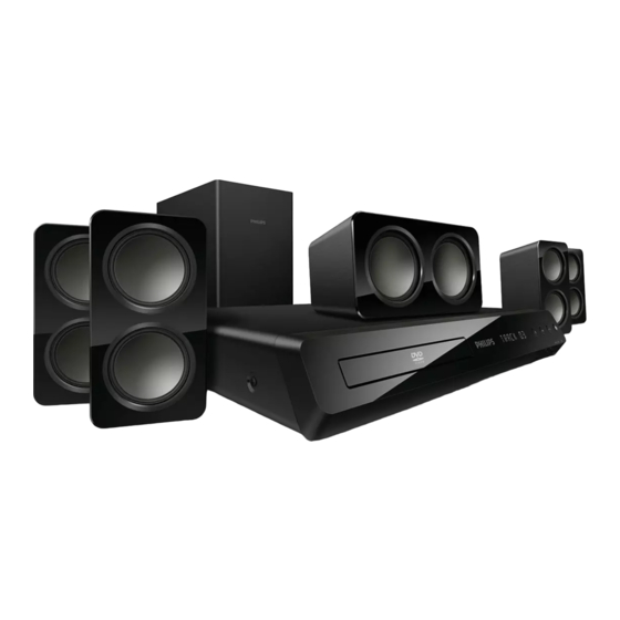
Home Theater DVD Player
Service
Service Manual
. Location of PCB BdsÿVersion Variation and Repair Scenario Matrix..........1-2
. Technical Specifications.........................................................1- 3
. Safety Instruction, Warning & Notes........................................1- 4
. DFU Instruction..............................................................................2-1
. Mechanical and Dismantling Instructions....................................3-1
. Software Upgrades .......................................................................
. Trouble Shooting Chart......................................................
. Wiring Diagram..................................................................6-1
. Electrical Diagrams and Print-layouts......................................7-1
. Set Mechanical Exploded view & Part list................................8-1
. Revision List..................................................................................9-1
©Copyright 2011 Philips Consumer Electronics B.V. Eindhoven, The Netherlands
All rights reserved. No part of this publication may be reproduced, stored in aretrieval system or
transmitted, in any form or by any means, electronic, mechanical, photocopying, or otherwise
without the prior permission of Philips.
Published by RY&WL - 1125 BU AVM Printed in The Netherlands Subject to modification
Version 1.1
TABLE OF CONTENTS
HTS3531/05/12/51/79/94/98
Page
4-1
.
5-1
.
CLASS 1
LASER PRODUCT
GB
PHILIPS
3139 785 35841
Advertisement

Related Manuals for Philips HTS3531/05


Summary of Contents for Philips HTS3531/05
-
Page 1: Table Of Contents
. Electrical Diagrams and Print-layouts..….…………………..….…7-1 . Set Mechanical Exploded view & Part list.…………………..….….8-1 . Revision List..................9-1 ©Copyright 2011 Philips Consumer Electronics B.V. Eindhoven, The Netherlands All rights reserved. No part of this publication may be reproduced, stored in aretrieval system or CLASS 1... - Page 2 PCB BOARD LOCATION: AMPLIFIER BOARD MAIN BOARD POWER BOARD LOADER FRONT CONTROL BOARD Version Variation Type/Versions HTS3531 Features Output Power-300W Voltage(220~240V) Voltage(110~240V) MP3 LINK Repair Scenario Matrix Type/Versions HTS3531 Board in used Main Board Front Control Board Amplifier Board Power Board *Bd:Board Level Replacement *C:Component Level Repair...
- Page 3 HTS3531/05/12/51/79/94/98: Product Specifications: Amplifi er Note • Total output power: 300W RMS (30% • Specifi cations and design are subject to change THD) without notice. • Frequency response: 20 Hz-20 kHz / ±3 dB • Signal-to-noise ratio: > 65 dB (CCIR) /...
- Page 4 Main unit • Power supply: • Europe/China/Russia/India: 220-240V, ~50 Hz • Latin America/Asia Pacifi c: 110-240V ~50-60 Hz • Power consumption: 55 W • Standby power consumption: 0.9 W • Dimensions (WxHxD): 360 x 58 x 325 mm • Weight: 2.3 kg Subwoofer •...
-
Page 5: Safety Instruction, Warning & Notes
Safety instruction, Warning & Notes Safety instruction 1. General safety 2.Laser safety Safety regulations require that during a repair: This unit employs a laser. Only qualified service personnel . Connect the unit to the mains via an isolation transformer. may remove the cover, or attempt to service this device . - Page 6 Warning 1.General 2. Laser . All ICs and many other semiconductors are susceptible to . The use of optical instruments with this product, will electrostatic discharges (ESD). Careless handing during increase eye hazard. repair can reduce life drastically. Make sure that, during .
- Page 7 Solder Joint...
- Page 8 - lead free BGA-ICs will be delivered in so-called respected by the workshop during a repair: ‘dry-packaging’ (sealed pack including a silica gel Use only lead-free solder alloy Philips SAC305 with pack) to protect the IC against moisture. After order code 0622 149 00106. If lead-free solder-paste is...
- Page 9 EN Before using your product, read all accompanying safety NO Les all vedlagt sikkerhetsinformasjon før du bruker information produktet DA Læs alle medfølgende sikkerhedsoplysninger, inden du PT Antes de utilizar o produto, leia todas as informações de tager produktet i brug segurança que o acompanham DE Lesen Sie vor Verwendung dieses Produkts alle SV Innan du använder produkten ska du läsa all tillhörande...
- Page 10 EN Connect the home theater ’ FRONT FRONT FRONT WOOFER LEFT RIGHT CENTER FRONT FRONT FRONT REAR REAR RIGHT LEFT CENTER RIGHT LEFT WOOFER REAR REAR LEFT RIGHT FRONT FRONT REAR REAR FRONT RIGHT LEFT RIGHT LEFT WOOFER CENTER...
- Page 11 HDMI OUT HDMI IN ANTENNA AC MAINS~...
- Page 12 EN Switch on the home theater...
- Page 13 EN Complete the fi rst time setup HDMI HOME THEATER Русский Українська HOME THEATER...
- Page 14 EN Use your home theater...
- Page 15 MUSIC iLINK...
- Page 16 HTS3531/05/12/51/79/94/98 Your home theater Remote control Congratulations on your purchase, and welcome to Philips! To fully benefi t from the support that This section includes an overview of the remote Philips offers, register your home theater at control. www.philips.com/welcome. Main unit...
- Page 17 ( Standby-On ) • Switch the home theater on or to REPEAT / PROGRAM standby. • Select or turn off repeat mode. • When EasyLink is enabled, press • In radio mode, set a radio station. and hold for at least three seconds to switch all connected HDMI CEC REPEAT A-B compliant devices to standby.
-
Page 18: Mechanical And Dismantling Instructions
Mechanical and Dismantling Instructions Dismantling Instruction Detailed information please refer to the model set. The following guidelines show how to dismantle the player. Step1: Remove 6 screws around the Top Cover, and then remove the Top Cover (Figure 1). Sample Model:HTS3531/12 Figure 1 Step2: If it is necessary to dismantle Loader or Front Panel, the Front door should be removed first. - Page 19 Mechanical and Dismantling Instructions Detailed information please refer to the model set. Dismantling Instruction :Dismantle Front Panel, disconnect the connectors (XP4, XP8,XP12), need release 2 snaps of Front Panel & 2 snaps Step3 of bottom cabinet , then gently pull the Panel out from the set. (Figure 3) Figure 3 Step4 : Dismantle Front Control Board,remove 5 screws (Figure 4...
- Page 20 Mechanical and Dismantling Instructions Dismantling Instruction Detailed information please refer to the model set. : Dismantle Main Board, first disconnect 2 connectors (XP1, XP11), and then remove 6 screws. (Figure 5/6) Step6 : Dismantle Power Board, disconnect the connector s XS703 and CN501 on Power Board,then remove 5 screws.(Figure 5/6) Step7 (Figure 5/6) Step8: Dismantle Amplifier Board, remove...
-
Page 21: Software Upgrades
Software upgrade A. Software upgrade method: 1. Set up a new folder and name it ’UPG’ in the root of USB device. 2. Copy the file(HTS_XXXX.bin)which you want to upgrade into the ‘UPG’ folder 3. Power on the BD Player, after it shows the UI, plug the USB device 4. -
Page 22: Trouble Shooting Chart
Trouble shooting Chart VFD No display on Front Control Board VFD No display on Front Control Board Check every supply voltage on Main Board whether normal or not. Refer to CN502 on Power Board (XP1 PIN1:-24V, PIN3: 12V, PIN5&PIN6: Check voltage -24V, +5V, +12V on Power Fix the connection HTS3531:XP2 on Board at CN502 position and Front Control Front Control Board... - Page 23 Trouble shooting Chart keys do not work keys do not work HTS3531: Fix the connection XP2 on Check voltage +3.3V on Front Control Board Front Control Board XP12 on HTS3531:(XP2 PIN9) and voltage +5V on U135 PIN14 MAIN BOARD Check Front Control Board signals (U135 Replace U135 on Front Control PIN10,PIN11,PIN12) Board...
- Page 24 Trouble shooting Chart Remote control does not work Remote control does not work Check battery of remote control whether Replace the battery for remote exhausted or not. control Check power supply of IR601 on Front Check the +3.3V net on Front Control Board whether normal or not Control Board HTS3531:XP2 HTS3531:XP2 PIN9 3.3V...
- Page 25 Trouble shooting Chart No audio output No audio output Check XP11 pin 14&16 3.3V on Main Check voltage +34.5 Board whether normal or not V whether normal or not at XP702 on Amplifier Board Refer to CN502 on Power Board Check the 24pin FFC connection XP11 on Main Board and XP701 on Amplifier Board whether right or not between Main Board...
- Page 26 Trouble shooting Chart No video output No video output Check L6 , R433 whether right on Main L6, R433 on Main Board Board Check the video signal whether right at U1: PIN139 Replace Main Board...
- Page 27 Trouble shooting Chart Can’t read disc or can’t open the disk door Can’t read disc or can’t open the disk door Check loader whether work normally Check XP1 on Main Board or not Check 24pin 6pin and 5pin cable from Main Board to Loader whether Fix 24pin 6pin and 5pin cable connect right or not Replace Loader...
- Page 28 Trouble shooting Chart Tuner FM does not work Tuner FM does not work Check voltage at Q6:+3.3V on Main Board whether normal or not Refer to Power Board CN502 Check voltage +3.3V at Tuner module (TUN1 pin5) whether right or Check Main Board tuner power supply circuit.
- Page 29 Trouble shooting Chart AUX in does not work AUX in does not work Check voltage at U12 PIN8:12V on Main Board whether normal or not Refer to Power Board CN502 Check Main Board U5 PIN2,PIN15 signal input whether right or not Check C166,C167,R87,R91 Check voltage at U5 74HC4052 PIN16, Check Main Board U1 power...
- Page 30 Trouble shooting Chart MP3 Link does not work MP3 Link does not work HTS3531:Check signal at XS605:PIN3:MP3_R PIN1:MP3_L ON front board whether normal Refer to Main Board XP8 or not Check Main Board 74HC4052 Check Main Board C169, C170, R103, PIN4,PIN11 L/R signal input whether right or not R105,...
- Page 31 5-10 Trouble shooting Chart OPTICAL IN does not work OPTICAL in does not work Check voltage at P2 PIN1:5V on Main Board whether normal or not Refer to Power Board CN502 Check Main Board P2 PIN3 signal input whether right or not Check Main Board C106, Replace U1...
-
Page 32: Wiring Diagram
HTS3531 BLOCK / WIRING DIAGRAM 4ohm 4ohm 4ohm 4ohm 4ohm 4ohm FM TUNER FAN control AUX L/R CVBS SPDIF Optical Fiber HDMI 10PIN2.0mm SDRAM HC4052 4558 MT1389GH-FXE AK5358 2PIN2.0mm I2S 6pin I2S 6pin RDS DATA I2S_SD0 I2C 1 I2S_LRCK I2S_SD1 I2S_SD2 XP701 I2S_BCLK... - Page 33 Front Control Board Circuit Diagram: +12V VFD_32P_VFD200824 VFD_32P_VFD200824 R135 R135 14PIN/1.0mm 14PIN/1.0mm +5VA +12VA R137 R137 R136 R136 R141 R141 MIC_DET R138 R138 Q135 Q135 Q136 Q136 NPN_3DG3904M NPN_3DG3904M FB613 FB613 500/800mA 500/800mA -24V NPN_3DG3904M NPN_3DG3904M FB604 FB604 500/800mA 500/800mA +12V FB609 FB609...
- Page 34 Amplifier Board Circuit Diagram:STA309A VD3.3V R800 R800 0/NC 0/NC D705 D705 Q702 Q702 LL4148 LL4148 PNP_MMBT8550CLT1 PNP_MMBT8550CLT1 VD3.3V R739 R739 C716 C716 0.1uF/25V/Y5V 0.1uF/25V/Y5V CE723 CE723 47uF/50V 47uF/50V ASDAT0 TP41 TP41 LRCLK R805 R805 Q701 Q701 D712 D712 C714 C714 ASDAT1 LL4148 LL4148...
- Page 35 Amplifier Board Circuit Diagram:STA518 L708 L708 10uH/5A 10uH/5A U701 U701 IC_36P_STA518 IC_36P_STA518 SUB- TP26 TP26 TP27 TP27 SUB+ VCC-Sign SUB-GND L702 L702 22uH/3.3A/NC 22uH/3.3A/NC TP28 TP28 TP29 TP29 VCC-Sign OUT2B C734 C734 C735 C735 TP30 TP30 TP31 TP31 0.1uF/50V/X7R 0.1uF/50V/X7R 0.1uF/50V/X7R 0.1uF/50V/X7R R718...
- Page 36 R540A R540A CY506 CY506 XP502 4PIN/2.5mm XP502 4PIN/2.5mm C533 C533 1500pF/1KV 1500pF/1KV R575 R575 Q571 Q571 Power Board Circuit Diagram: R540B R540B 470pF/250VAC 470pF/250VAC PNP_MMBT8550CLT1 PNP_MMBT8550CLT1 M+5V R540C R540C T531 T531 PQ3230 PQ3230 R578 R578 Alternative L531 L531 T531P +33V CN531 CN531 6PIN/2.5mm/70mm...
- Page 37 Main Board Circuit Diagram: Power Supply +12V: +12V(+-10%) +5V: +5V(+-2.5%) OFF-PAGE CONNECTION TO POWER BOARD URST# URST# MO_VCC AVCC POWER_ON/OFF POWER_ON/OFF AVCC C125 C125 300/2A 300/2A 0.1uF/25V/Y5V 0.1uF/25V/Y5V 0/NC 0/NC 500/500mA 500/500mA MO_VCC 0.1uF/25V/Y5V 0.1uF/25V/Y5V 47uF/16V 47uF/16V 0.1uF/25V/Y5V 0.1uF/25V/Y5V PNP_PBSS5320T PNP_PBSS5320T 0603 8PIN/2.5mm...
- Page 38 OFF-PAGE CONNECTION Main Board Circuit Diagram:MT1389GH DQ[0..15] DQ[0..15] MA[0..11] MA[0..11] 89G_3V3 0.1uF/25V/Y5V 0.1uF/25V/Y5V DQM[0..1] DQM[0..1] 89G_3V3 Crystal 4.7uF/10V/Y5V 4.7uF/10V/Y5V BA[0..1] 100K 100K BA[0..1] 0.1uF/25V/Y5V 0.1uF/25V/Y5V BAT54C BAT54C RFV12-1 RFVDD3 DACVDD3 DACVDD3 ADACVDD SP-A 0.1uF/25V/Y5V 0.1uF/25V/Y5V DCLK DCLK 500/500mA 500/500mA 500/500mA 500/500mA 500/500mA 500/500mA...
- Page 39 Main Board Circuit Diagram:SDRAM & FLASH OFF-PAGE CONNECTION DV33 FB19 FB19 500/500mA 500/500mA SR_3V3 DQ[0..15] DQ[0..15] SR_3V3 FB20 FB20 500/500mA 500/500mA MA[0..11] MA[0..11] SDCKE CE24 CE24 DQM[0..1] DQM[0..1] DCKE SDCKE 100uF/25V 100uF/25V 0.1uF/25V/Y5V 0.1uF/25V/Y5V BA[0..1] BA[0..1] DCLK DCLK DCS# MA10 DQ10 RAS# RAS#...
- Page 40 Main Board Circuit Diagram:AUDIO IN +6VA +6VA AL_CH3 R164 R164 150K 150K 1uF/50V/Y5V 1uF/50V/Y5V R162 R162 1uF/50V/Y5V 1uF/50V/Y5V TUNER_L C163 C163 AL_CH2 AR_CH3 R165 R165 150K 150K AUX2_L C166 C166 AL_CH3 OFF-PAGE CONNECTION R154 R154 CE30 CE30 R118 R118 0.1uF/25V/Y5V 0.1uF/25V/Y5V AL_CH4 R173...
- Page 41 Main Board Circuit Diagram:VIDEO I/F AVCC R125 R125 SCART16 1.2uH/25mA 1.2uH/25mA NPN_3DG3904M NPN_3DG3904M OFF-PAGE CONNECTION R126 R126 R127 R127 0.1uF/25V/Y5V 0.1uF/25V/Y5V R128 R128 4.7K 4.7K 100pF/50V/NP0 100pF/50V/NP0 R129 R129 2.2K 2.2K SCART_CON SCART_CON SCART16 SCART_CON CVBS_OUT CVBS_OUT 1.2uH/25mA 1.2uH/25mA 1.5K 1.5K R130 R130...
- Page 42 7-10 7-10 Main Board Circuit Diagram:AMP / FB / TUNER ASDAT0 LRCK TUNER_13P_A TUNER_13P_A ASDAT1 ASDAT2 TU_RST R185 R185 TU_RST /RST AGND /SEN R186 R186 TU_SCL SCLK TU_SCL AM_SCL R187 R187 TU_SDA TU_SDA AM_SCL SDIO AM_SDA FB25 500/500mA FB25 500/500mA AM_SDA VCC(+5V) AMP_MUTE...
- Page 43 7-11 7-11 Front Control Board Print-layout (top side):...
- Page 44 7-12 7-12 Amplifier Board Print-layout (top side):...
- Page 45 7-13 7-13 Amplifier Board Print-layout (bottom side):...
- Page 46 7-14 7-14 Power Supply Print-layout (top side):...
- Page 47 7-15 7-15 7-15 Main Board Print-layout (top side):...
- Page 48 7-16 7-16 Main Board Print-layout (bottom side):...
- Page 49 EXPLODED VIEW FOR HTS3531/05/12/51/79/94/98 ASSY1 This is general mechanical exploded view .Please refer to the model set for the detailed information. ASSY1 includes components:15,16,17,19,24...
-
Page 50: Revision List
REVISION LIST Version 1.0 * Initial release for HTS3531/12/51/94/98 Version 1.1 * Adding HTS353/05/79...
Need help?
Do you have a question about the HTS3531/05 and is the answer not in the manual?
Questions and answers