Table of Contents
Advertisement
Colour Television
Contents
11. Styling Sheets
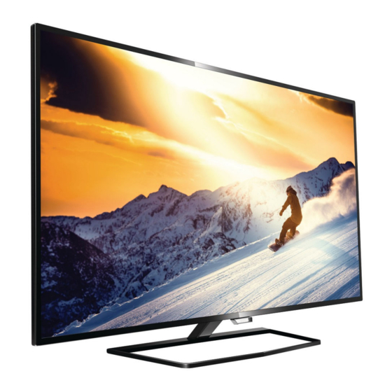
5011 series 32"
5011 series 40"
Published by XMM/CQZ/SC 1622 Quality
©
2016
TP Vision Netherlands B.V.
All rights reserved. Specifications are subject to change without notice. Trademarks are the
property of Koninklijke Philips Electronics N.V. or their respective owners.
TP Vision Netherlands B.V. reserves the right to change products at any time without being obliged to adjust
earlier supplies accordingly.
PHILIPS and the PHILIPS' Shield Emblem are used under license from Koninklijke Philips Electronics N.V.
Page
Contents
2
2
5
9
9
10
22
24
32
35
Drawing PWB
36
38-39
40
44-45
46
61-62
63
64
65
66
67
71-72
73
74
Printed in the Netherlands
Chassis
TPM16.4HE
Page
Subject to modification
EN 3122 785 20001
LA
Advertisement
Table of Contents


Need help?
Do you have a question about the 40HFL5011T/12 and is the answer not in the manual?
Questions and answers