
Related Manuals for Jameco Atmel AT89C2051

Summary of Contents for Jameco Atmel AT89C2051
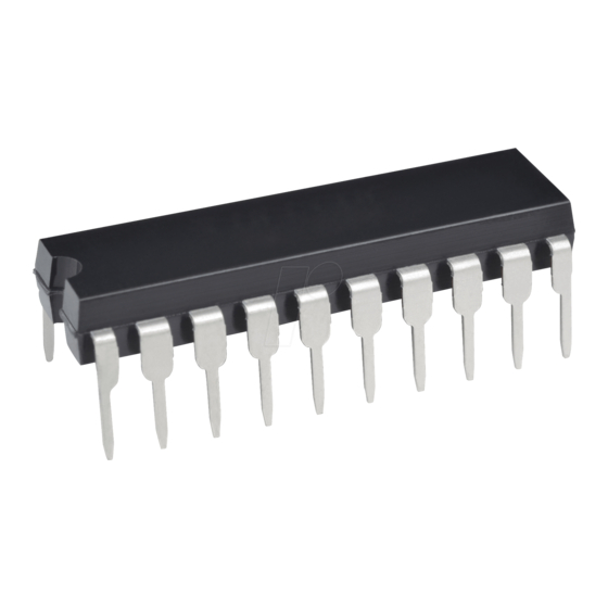
- Page 1 Distributed by: www.Jameco.com 1-800-831-4242 The content and copyrights of the attached material are the property of its owner.
-
Page 2: Pin Configuration
MCS-51™ instruction set. By combining a versatile 8-bit CPU with Flash on a monolithic chip, the Atmel AT89C2051 is a pow- erful microcomputer which provides a highly flexible and cost effective solution to many embedded control applications. -
Page 3: Block Diagram
Block Diagram AT89C2051 4-16... -
Page 4: Pin Description
AT89C2051 Pin Description XTAL2 Output from the inverting oscillator amplifier. Supply voltage. Oscillator Characteristics XTAL1 and XTAL2 are the input and output, respectively, Ground. of an inverting amplifier which can be configured for use as Port 1 an on-chip oscillator, as shown in Figure 1. Either a quartz Port 1 is an 8-bit bidirectional I/O port. -
Page 5: Special Function Registers
Special Function Registers A map of the on-chip memory area called the Special Func- User software should not write 1s to these unlisted loca- tion Register (SFR) space is shown in the table below. tions, since they may be used in future products to invoke new features. - Page 6 AT89C2051 Restrictions on Certain Instructions Program Memory Lock Bits The AT89C2051 and is an economical and cost-effective On the chip are two lock bits which can be left unpro- member of Atmel’s growing family of microcontrollers. It grammed (U) or can be programmed (P) to obtain the addi- contains 2K bytes of flash program memory.
-
Page 7: Programming The Flash
Programming The Flash Ready/Busy: The Progress of byte programming can also be monitored by the RDY/BSY output signal. Pin P3.1 is The AT89C2051 is shipped with the 2K bytes of on-chip pulled low after P3.2 goes High during programming to indi- PEROM code memory array in the erased state (i.e., con- cate BUSY. - Page 8 AT89C2051 Flash Programming Modes Mode RST/VPP P3.2/PROG P3.3 P3.4 P3.5 P3.7 (1)(3) Write Code Data Read Code Data Write Lock Bit - 1 Bit - 2 Chip Erase Read Signature Byte Notes: 1. The internal PEROM address counter is reset to 000H on the rising edge of RST and is advanced by a positive pulse at XTAL 1 pin.
- Page 9 Flash Programming and Verification Characteristics = 5.0 ± 10% = 0°C to 70°C, V Symbol Parameter Units Programming Enable Voltage 11.5 12.5 µA Programming Enable Current µs Data Setup to PROG Low DVGL µs Data Hold After PROG GHDX µs P3.4 (ENABLE) High to V EHSH µs...
-
Page 10: Absolute Maximum Ratings
AT89C2051 Absolute Maximum Ratings* *NOTICE: Stresses beyond those listed under “Absolute Operating Temperature ......... -55°C to +125°C Maximum Ratings” may cause permanent dam- age to the device. This is a stress rating only and Storage Temperature ........-65°C to +150°C functional operation of the device at these or any Voltage on Any Pin other conditions beyond those indicated in the... -
Page 11: External Clock Drive Waveforms
External Clock Drive Waveforms External Clock Drive Symbol Parameter = 2.7V to 6.0V = 4.0V to 6.0V Units Oscillator Frequency CLCL Clock Period 83.3 41.6 CLCL High Time CHCX Low Time CLCX Rise Time CLCH Fall Time CHCL AT89C2051 4-24... - Page 12 AT89C2051 Serial Port Timing: Shift Register Mode Test Conditions = 5.0V ± 20%; Load Capacitance = 80 pF) Symbol Parameter 12 MHz Osc Variable Oscillator Units µs Serial Port Clock Cycle Time XLXL CLCL Output Data Setup to Clock Rising Edge -133 QVXH CLCL...
- Page 13 AT89C2051 TYPICAL ICC - ACTIVE (85°C) Vcc=6.0V Vcc=5.0V Vcc=3.0V FREQUENCY (MHz) AT89C2051 TYPICAL ICC - IDLE (85°C) Vcc=6.0V Vcc=5.0V Vcc=3.0V FREQUENCY (MHz) AT89C2051 TYPICAL ICC vs. VOLTAGE- POWER DOWN (85°C) µ 3.0V 4.0V 5.0V 6.0V Vcc VOLTAGE Notes: XTAL1 tied to GND for I (power down) P .1.0 and P1.1 = V or GND...
-
Page 14: Ordering Information
AT89C2051 Ordering Information Speed Power (MHz) Supply Ordering Code Package Operation Range 2.7V to 6.0V AT89C2051-12PC 20P3 Commercial AT89C2051-12SC (0°C to 70°C) AT89C2051-12PI 20P3 Industrial AT89C2051-12SI (-40°C to 85°C) AT89C2051-12PA 20P3 Automotive AT89C2051-12SA (-40°C to 105°C) 4.0V to 6.0V AT89C2051-24PC 20P3 Commercial AT89C2051-24SC...
Need help?
Do you have a question about the Atmel AT89C2051 and is the answer not in the manual?
Questions and answers