Table of Contents
Advertisement
RX-V520/RX-V520RDS/
HTR-5450/HTR-5450RDS
This manual has been provided for the use of authorized YAMAHA Retailers and their service personnel.
It has been assumed that basic service procedures inherent to the industry, and more specifically YAMAHA Products, are already
known and understood by the users, and have therefore not been restated.
WARNING:
IMPORTANT:
The data provided is believed to be accurate and applicable to the unit(s) indicated on the cover. The research, engineering, and
service departments of YAMAHA are continually striving to improve YAMAHA products. Modifications are, therefore, inevitable
and specifications are subject to change without notice or obligation to retrofit. Should any discrepancy appear to exist, please
contact the distributor's Service Division.
WARNING:
IMPORTANT:
I CONTENTS
TO SERVICE PERSONNEL .......................................... 1
IMPEDANCE SELECTOR ............................................. 1
FRONT PANELS ............................................................ 2
REAR PANELS .......................................................... 3~4
SPECIFICATIONS .......................................................... 5
INTERNAL VIEW ........................................................... 6
DISASSEMBLY PROCEDURES ................................... 7
SELF DIAGNOSIS FUNCTION (DIAG) ................... 8~24
1 0 0 7 5 5
RX-V520RDS
D I G I T A L
STANDBY
SURROUND
/ON
BASS
TREBLE
BALANCE
SPEAKERS
A
B
+
+
-
-
L
R
ON
OFF
Failure to follow appropriate service and safety procedures when servicing this product may result in personal
injury, destruction of expensive components, and failure of the product to perform as specified. For these reasons,
we advise all YAMAHA product owners that any service required should be performed by an authorized
YAMAHA Retailer or the appointed service representative.
The presentation or sale of this manual to any individual or firm does not constitute authorization, certification or
recognition of any applicable technical capabilities, or establish a principle-agent relationship of any form.
Static discharges can destroy expensive components. Discharge any static electricity your body may have
accumulated by grounding yourself to the ground buss in the unit (heavy gauge black wires connect to this buss).
Turn the unit OFF during disassembly and part replacement. Recheck all work before you apply power to the unit.
AV RECEIVER
SERVICE MANUAL
D I G I T A L
EFFECT
PRESET/TUNING
A/B/C/D/E
PROGRAM
PHONES
S VIDEO
VIDEO
L
AUDIO R
OPTICAL
SILENT
VIDEO AUX
IMPORTANT NOTICE
AMP ADJUSTMENTS .................................................. 24
DISPLAY DATA ..................................................... 25~26
IC DATA ................................................................. 27~32
BLOCK DIAGRAM ................................................. 33~36
PRINTED CIRCUIT BOARD .................................. 37~52
IC BLOCK DIAGRAM ............................................ 53~54
SCHEMATIC DIAGRAM ........................................ 55~58
PARTS LIST ........................................................... 59~73
REMOTE CONTROL TRANSMITTER .................. 74~76
VOLUME
RDS MODE/FREQ
EON
PTY SEEK
MODE
START
INPUT MODE
6CH INPUT
PRESET
/TUNING
FM/AM
INPUT
EDIT
TUNING
MEMORY
MODE
MAN'L/AUTO FM AUTO/MAN'L MONO
P.O.Box 1, Hamamatsu, Japan
Advertisement
Table of Contents

Related Manuals for Yamaha HTR-5450


Summary of Contents for Yamaha HTR-5450
-
Page 1: Table Of Contents
This manual has been provided for the use of authorized YAMAHA Retailers and their service personnel. It has been assumed that basic service procedures inherent to the industry, and more specifically YAMAHA Products, are already known and understood by the users, and have therefore not been restated. -
Page 2: To Service Personnel
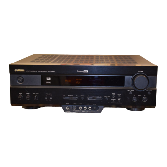
RX-V520/RX-V520RDS/HTR-5450/HTR-5450RDS I TO SERVICE PERSONNEL 1. Critical Components Information AC LEAKAGE Components having special characteristics are marked s WALL EQUIPMENT TESTER OR and must be replaced with parts having specifications equal OUTLET UNDER TEST EQUIVALENT to those originally installed. 2. Leakage Current Measurement (For 120V Models Only) - Page 3 MAN'L/AUTO FM AUTO/MAN'L MONO PHONES S VIDEO VIDEO AUDIO R OPTICAL SILENT VIDEO AUX HTR-5450 (U, C, A, R, T models) VOLUME HTR-5450 D I G I T A L D I G I T A L SURROUND STANDBY INPUT MODE...
-
Page 4: Rear Panels
RX-V520/RX-V520RDS/HTR-5450/HTR-5450RDS I REAR PANELS U model C model A model B model... - Page 5 RX-V520/RX-V520RDS/HTR-5450/HTR-5450RDS G model L model R, T model...
-
Page 6: Specifications
RX-V520/RX-V520RDS/HTR-5450/HTR-5450RDS I SPECIFICATIONS I Audio Section Monitor Out Frequency Response S-Video Signal Level ......... 5 Hz to 10 MHz, -3 dB Minimum RMS Output Power (Power Amp. Section) I FM Section (20 Hz to 20 kHz, 0.06% THD, 8 ohms) -
Page 7: Internal View
RX-V520/RX-V520RDS/HTR-5450/HTR-5450RDS • Set Menu Table SET MENU PRESET VALUE SETTING RANGES SPEAKER SET CENTER SPEAKER LARGE LARGE/SMALL/NONE MAIN SPEAKER LARGE LARGE/SMALL REAR L/R SPEAKER LARGE LARGE/SMALL/NONE LFE/BASS OUT BOTH SUBWOOFER/MAIN/BOTH MAIN LEVEL NORMAL NORMAL/–10dB HP TONE CTRL BASS : 0dB –6dB —... -
Page 8: Disassembly Procedures
RX-V520/RX-V520RDS/HTR-5450/HTR-5450RDS I DISASSEMBLY PROCEDURES (Remove parts in the order as numbered.) Disconnect the power cord from the AC outlet. 1. Removal of Top Cover (Fig. 1) Top Cover a. Remove 4 screws (1) and 4 screws (2). b. Slide the Top Cover rearward to remove it. -
Page 9: Self Diagnosis Function (Diag)
RX-V520/RX-V520RDS/HTR-5450/HTR-5450RDS I SELF DIAGNOSIS FUNCTION (DIAG) There are 14 DIAG menu items each of which has sub-menu items. Listed in the table below are menu items and sub-menu items. No DIAG menu sub-menu Remote control code (key) DSP THROUGH 1. ANALOG BYPASS 7A-88 (PRG 1) 2. - Page 10 RX-V520/RX-V520RDS/HTR-5450/HTR-5450RDS • Starting DIAG Press the “POWER ” (STANDBY/ON) key of the main unit while pressing the Keys of main unit “FM/AM ” key and the “INPUT MODE ” key simultaneously, and DIAG will be INPUT MODE activated. FM/AM • Starting DIAG in the protection cancel mode...
- Page 11 RX-V520/RX-V520RDS/HTR-5450/HTR-5450RDS PS PRT display (When the power is turned on without this abnormality corrected, the protection function activates about 1 second later to shut off the power relay. Display may not light if there is an abnormality with the power supply for the display.) Cause: There is an abnormality in the power supply section (voltage).
- Page 12 RX-V520/RX-V520RDS/HTR-5450/HTR-5450RDS • Initial settings used to start DIAG function Following initial settings are used when starting the DIAG function. When the DIAG function is canceled, the settings before starting DIAG will be restored. • Input : DVD (6CH INPUT OFF) •...
- Page 13 RX-V520/RX-V520RDS/HTR-5450/HTR-5450RDS M, C, R, SW CH [Remote control code: 7A-89 (PRG 2)] • The input signal is automatically identified and switched in the priority order of dts ➔ DOLBY DIGITAL ➔ PCM AUDIO ➔ Analog (A/D) according to the signal detection.
- Page 14 RX-V520/RX-V520RDS/HTR-5450/HTR-5450RDS MAIN HPF [Remote control code: 7A-8A (PRG 3)] • MAIN HPF is turned on and output. (Head margin included) Head margin: L/R: 0/-3/-12/-18dBFS, Center: Mute, RL/RR: Mute, SWFR: Mute. Reference data INPUT: DVD ANALOG SWFR: 50Hz, Others: 1kHz Condition...
- Page 15 RX-V520/RX-V520RDS/HTR-5450/HTR-5450RDS FULL BIT F [Remote control code: –] • The front channel signal is output in full bit to the main channel. Reference data INPUT: DVD ANALOG SWFR: 50Hz, Others: 1kHz Condition MAIN L/R CENTER RL/RR SWFR Both ch, -20 dBV, volume -10 dB 22.5 dBV 16.0 dBV 22.0 dBV 13.5 dBV...
- Page 16 RX-V520/RX-V520RDS/HTR-5450/HTR-5450RDS 2. FRONT CH The input signal is automatically identified and switched in the priority order of dts ➔ DOLBY DIGITAL ➔ PCM AUDIO ➔ Analog (A/D) according to the signal detection. The front channel signal is output in full bit to the main channel.
- Page 17 RX-V520/RX-V520RDS/HTR-5450/HTR-5450RDS 3. RAM THROUGH The input signal is automatically identified and switched in the priority order of dts ➔ DOLBY DIGITAL ➔ PCM AUDIO ➔ Analog (A/D) according to the signal detection. The Center and RL/RR signals are output through the external DRAM.
- Page 18 RX-V520/RX-V520RDS/HTR-5450/HTR-5450RDS [2ch] *Multi: All Mute AC3D3 YSS928 Main DSP Sub DSP (Decoder) ANALOG CODEC CODEC SDOB2 -3dB (A/D) (D/A) AK4527 AK4527 INTERNAL C/Mute SDOB1 -3dB/Mute SWFR DIGITAL SDOB3 -12dB 4M DRAM 5. MARGIN CHECK The input signal is automatically identified and switched in the priority order of dts ➔ DOLBY DIGITAL ➔ PCM AUDIO ➔...
- Page 19 RX-V520/RX-V520RDS/HTR-5450/HTR-5450RDS 6. MAIN MIX The input signal is automatically identified and switched in the priority order of dts ➔ DOLBY DIGITAL ➔ PCM AUDIO ➔ Analog (A/D) according to the signal detection. There are 2 sub-menu items. The center and SW signals are output through the main channel.
- Page 20 RX-V520/RX-V520RDS/HTR-5450/HTR-5450RDS 7. OTHER INPUT The signal inputted through the 6CH INPUT terminals is output. EXTERNAL DECODER [Remote control code: 7A-8F (PRG 8)] Reference data INPUT: 6CH INPUT SWFR: 50Hz, Others: 1kHz Condition MAIN L/R CENTER RL/RR SWFR Both ch, -20 dBV, volume -10 dB 13.5 dBV 13.5 dBV 13.5 dBV -7.0 dBV 8.
- Page 21 RX-V520/RX-V520RDS/HTR-5450/HTR-5450RDS 10. PRESET This menu is used to reserve and inhibit initialization of the back-up RAM. The signals are processed using EFFECT OFF. (The L/R signal is output using ANALOG MAIN BYPASS.) PRESET INHIBIT (Initialization inhibited) [REMOTE CONTROL CODE: –] RAM initialization is not executed.
- Page 22 RX-V520/RX-V520RDS/HTR-5450/HTR-5450RDS 11. AD DATA CHECK This menu is used to display the A/D conversion value of the main CPU which detects panel keys of the main unit and protection functions in % using the sub-menu. (Reference voltage 5V as 100%) During signal processing, the condition before execution is maintained.
- Page 23 RX-V520/RX-V520RDS/HTR-5450/HTR-5450RDS 12. IF STATUS Using the sub-menu, the status data is displayed one after another in the hexadecimal notation. During signal processing, the status before execution of this menu is maintained. * Numeric values in the figure example are for reference.
- Page 24 RX-V520/RX-V520RDS/HTR-5450/HTR-5450RDS CS1-5 [Remote control code: -]: Indicates channel status information of the input signal (IEC60958). BI1-4 [Remote control code: -]: Indicates bit stream information included in the DOLBY DIGITAL signal. BS1-4 [Remote control code: -]: Indicates bit stream information included in the dts signal.
-
Page 25: Amp Adjustments
RX-V520/RX-V520RDS/HTR-5450/HTR-5450RDS 14. MICROPROCESSOR INFORMATION There are 3 sub-menu items. The version, checksum and the port specified by the microprocessor are displayed. The signal is processed using EFFECT OFF. The checksum is obtained by adding the data at every 16 bits for each program area and expressing the result as a 4- figure hexadecimal data. - Page 26 RX-V520/RX-V520RDS/HTR-5450/HTR-5450RDS I DISPLAY DATA G V301 : 10-BT-235GNK (V6840400) PATTERN AREA G PIN CONNECTION Pin No. 50 49 48 47 46 45 44 43 42 41 40 39 38 37 36 35 34 33 32 31 30 29 28 27 26...
- Page 27 RX-V520/RX-V520RDS/HTR-5450/HTR-5450RDS G ANODE CONNECTION (RT) (CT) (PS) (PTY) – – – – – – – – – – – – – – – – – – – – – – – – – – – – – – – –...
- Page 28 RX-V520/RX-V520RDS/HTR-5450/HTR-5450RDS I IC DATA IC801 : YSS928 RAMA9 RAMA3 SELI1 RAMA4 SELI0 SELI9 SELOA SELI10 SELOB SELI11 TESTMS SELI12 TESTXEN SELI13 IPORT0 RAMA2 IPORT1 RAMA5 IPORT2 RAMA1 IPORT3 RAMA6 IPORT4 RAMA0 DDIN0 RAMA7 DDIN1 RAMA8 DDIN2 VDD1 DDIN3 RASN RAMOEN...
- Page 29 RX-V520/RX-V520RDS/HTR-5450/HTR-5450RDS IC801 : YSS928 Pin Description Name Function Crystal oscillator connecting terminal Crystal oscillator connecting terminal (24.576MHz ) SELI1 Built-in selector input 1 (AXD) SELI0 Built-in selector input 0 (GND) SELOA Built-in selector output A (ISEL) SELOB Built-in selector output B...
- Page 30 RX-V520/RX-V520RDS/HTR-5450/HTR-5450RDS Name Function SDWCKI1 Word clock input terminal for SDIB, SDOB interface (Unconnected) SDBCKI1 Bit clock input terminal for SDIB, SDOB interface (Unconnected) Ground terminal SDOB3 PCM output terminal from Sub DSP SDOB2 PCM output terminal from Sub DSP SDOB1...
- Page 31 RX-V520/RX-V520RDS/HTR-5450/HTR-5450RDS Name Function RAMA5 Sub DSP: External memory address terminal 5 RAMA2 Sub DSP: External memory address terminal 2 SELI13 Built-in selector input 13 (Unconnected) SELI12 Built-in selector input 12 (Unconnected) SELI11 Built-in selector input 11 (Unconnected) SELI10 Built-in selector input 10 (Unconnected)
- Page 32 RX-V520/RX-V520RDS/HTR-5450/HTR-5450RDS IC902 : µPD78F4218AGF-3BA 16bit µ-COM (Main CPU) P85/A5 P06/INTP6 P86/A6 P05/INTP5 P87/A7 P04/INTP4 P40/AD0 P03/INTP3 P41/AD1 P02/INTP2/NMI P42/AD2 P01/INTP1 P43/AD3 P00/INTP0 P44/AD4 RESET P45/AD5 P46/AD6 P47/AD7 P50/A8 P51/A9 P52/A10 P53/A11 P127/RTP7 P54/A12 P126/RTP6 P55/A13 P125/RTP5 P56/A14 P124/RTP4 P57/A15 P123/RTP3...
- Page 33 RX-V520/RX-V520RDS/HTR-5450/HTR-5450RDS/DSP-AX520 IC902 : µPD78F4218AGF-3BA Pin Description No. PORT Function name I/O Detail of function No. PORT Function name I/O Detail of function 1 P60/A16 100 Vss 2 P61/A17 99 P57/A15 O Serial CE for sanyo device 3 P62/A18 98 P56/A14...
- Page 34 RX-V520/RX-V520RDS/HTR-5450/HTR-5450RDS/DSP-AX520 I BLOCK DIAGRAM (1/2) T161 D163 See page E-57/J-53 (DSP) XL801 COAXIAL IC801 YSS928 IC808A IC808B Q161 See page E-55/J-51 (INPUT) SIGNAL CXDTA DETECTOR D401 IC808C Q371 IC374 D403 OPTICAL OPTB MD/CD-R Q372 IC815A OPTC SDOB1 IC373 +12A –...
-
Page 35: Block Diagram
RX-V520/RX-V520RDS/HTR-5450/HTR-5450RDS/DSP-AX520 I BLOCK DIAGRAM (2/2) CONTROL C-INPUT SELECTOR D-TV/CBL IC302 Y-INPUT SELECTOR IC301 HP-RELAY V1, V2 VIDEO SP-RELAY XL901 10MHz 87-90 Q302, 305 Q301, 303 Q304, 306 IC903 POWER DETECT /RESET Q909, Q910 MAIN V1, 2 IC902 uPD78F4218AGF INPUT SELECTOR... - Page 36 RX-V520/RX-V520RDS/HTR-5450/HTR-5450RDS/DSP-AX520 To DSP • Semiconductor Location I PRINTED CIRCUIT BOARD (Foil side) Ref. No. Location D441 To INPUT (6) D442 INPUT (1) P. C. B. D443 From Tuner D444 D445 To OPERATION (5) D446 D447 D448 IC441 IC442 IC443 IC444...
-
Page 37: Printed Circuit Board
RX-V520/RX-V520RDS/HTR-5450/HTR-5450RDS/DSP-AX520 • Semiconductor Location I PRINTED CIRCUIT BOARD (Foil side) Ref. No. Location D371 INPUT (2) P. C. B. INPUT (3) P. C. B. INPUT (6) P. C. B. D372 D401 D402 MONITOR MONITOR CENTER/ D403 D-TV/CBL D-TV/CBL DVD MAIN REAR S. - Page 38 RX-V520/RX-V520RDS/HTR-5450/HTR-5450RDS/DSP-AX520 • Semiconductor Location I PRINTED CIRCUIT BOARD (Foil side) Ref. No. Location Circuit No. U, C R, T A, L B, G D901 J901 J902 D902 J903 D903 J904 J1005 D904 R908 R909 D905 R916, 919, 920 OPERATION (1) P. C. B.
- Page 39 RX-V520/RX-V520RDS/HTR-5450/HTR-5450RDS/DSP-AX520 I PRINTED CIRCUIT BOARD (Foil side) OPERATION (3) P. C. B. OPERATION (4) P. C. B. OPERATION (6) P. C. B. To INPUT (1) BASS TREBLE BALANCE To INPUT (4) To INPUT (1) +12A +12B To OPERATION (1) OPERATION (7) P. C. B.
- Page 40 RX-V520/RX-V520RDS/HTR-5450/HTR-5450RDS/DSP-AX520 I PRINTED CIRCUIT BOARD (Foil side) From INPUT (1) DSP P. C. B. (Lead Type Device) COAXIAL OPTICAL D-TV/CBL DIGITAL INPUT OPTICAL OPTICAL MD/CD-R OPTICAL DIGITAL MD/CD-R OUTPUT • Semiconductor Location Ref. No. Location Ref. No. Location Ref. No.
- Page 41 RX-V520/RX-V520RDS/HTR-5450/HTR-5450RDS/DSP-AX520 I PRINTED CIRCUIT BOARD (Foil side) DSP P. C. B. (Surface Mount Device) • Semiconductor Location Ref. No. Location Ref. No. Location Ref. No. Location Ref. No. Location D803 D818 D832 IC816 D804 D819 IC805 IC817 D805 D820 IC806...
- Page 42 RX-V520/RX-V520RDS/HTR-5450/HTR-5450RDS/DSP-AX520 I PRINTED CIRCUIT BOARD (Foil side) From MAIN (2) From From To MAIN (4) MAIN (1) P. C. B. OPERATION (5) OPERATION MAIN (5) REAR PRV1 CENTER NFRR NFRL From OPERATION From MAIN (2) • Semiconductor Location Ref. No.
- Page 43 RX-V520/RX-V520RDS/HTR-5450/HTR-5450RDS/DSP-AX520 I PRINTED CIRCUIT BOARD (Foil side) MAIN (2) P. C. B. MAIN (3) P. C. B. MAIN (4) P. C. B. SPEAKERS To MAIN (7) From AC power cord To MAIN (5) From MAIN (7) – – VOLTAGE SELECTOR...
-
Page 44: Ic Block Diagram
RX-V520/RX-V520RDS/HTR-5450/HTR-5450RDS/DSP-AX520 IC442: LC78213 IC446, 447: M5220L IC802: MSM514260C-60JS IC812: AK4527VQ I IC BLOCK DIAGRAM Analog Function Switch Dual OP-Amp. 4Mbit DRAM 24bit CODEC Audio Timing LIN+ Generator LIN- IC301, 302, 351: LA7956 RIN+ Controller Video Switch LCAS LCOM1 RCOM1 RIN-... -
Page 45: Schematic Diagram
RX-V520/RX-V520RDS/HTR-5450/HTR-5450RDS/DSP-AX520 SCHEMATIC DIAGRAM (INPUT) PIN CONNECTION DIAGRAM OF TRANSISTORS, DIODES AND ICS. 23.7 32.2 1P82 24.3 NJM7805FA NJM79M12FA 2SC1815 2SC1740S 2SA1708 1SS133 S1VB20 24.3 2SC2878 DTA144ES 2SC4488 1SS176 NJM7812FA Anode HZS11B2TD MTZJ5.6B 33.2 -24.8 -0.1 -0.1 – -24.8 Cathode -33.1 -24.2... - Page 46 RX-V520/RX-V520RDS/HTR-5450/HTR-5450RDS/DSP-AX520 SCHEMATIC DIAGRAM (OPERATION) MAIN L 11.9 FL DISPLAY FL DRIVER -29.5 -29.2 CENTER -11.8 -29.2 11.9 -29.2 3.3/50 -29.2 -29.2 -29.5 3.3/50 -11.8 11.9 3.3/50 3.3/50 -11.8 MAIN µ–COM 11.9 &4 -50.6 -51.4 -1.1 -50.6 12.7 -51.1 -52.6 -51.4 -52.6...
- Page 47 RX-V520/RX-V520RDS/HTR-5450/HTR-5450RDS/DSP-AX520 SCHEMATIC DIAGRAM (DSP) From INPUT (1) E-00/J-00 PIN CONNECTION DIAGRAM OF TRANSISTORS, DIODES AND ICS. 2SC3326 1SS355 µPC29M33T-E1 PQ025EZ5MZP M5220FP TC74HC00AF MSM514260C-60JS AK4527VQ NJM2904M TC74HCU04AF DTA144EK RB501V-40 TC74VHCT08AF Anode REGULATOR 3: IN 2: COM Cathode 1: OUT 2.5 4.4 4.5 MAIN L -20.2...
- Page 48 RX-V520/RX-V520RDS/HTR-5450/HTR-5450RDS/DSP-AX520 SCHEMATIC DIAGRAM (MAIN) 52.5 52.5 52.2 -0.4 -1.1 -0.5 -0.5 -1.1 -52.6 -52.6 MAIN L POWER AMP 52.5 52.5 52.2 -0.4 -1.1 -0.5 -0.5 26.9 13.8 -1.1 -52.6 -52.6 MAIN L MAIN R POWER AMP POWER RELAY 52.5 -29.4 -36.1...
-
Page 49: Parts List
RX-V520/RX-V520RDS/HTR-5450/HTR-5450RDS I WARNING PARTS LIST Components having special characteristics are marked s and must be replaced with parts having specifications equal to those originally in- stalled. I ELECTRICAL PARTS Carbon resistors (1/6W or 1/4W) are not included in the ELECTRICAL PARTS List. - Page 50 RX-V520/RX-V520RDS/HTR-5450/HTR-5450RDS P.C.B. INPUT Schm Schm Ref. PART NO. Description Markets Ref. PART NO. Description Markets V7261400 P.C.B. INPUT UCAL C380 UR838100 C.EL 100uF 16V V7261500 P.C.B. INPUT C381 UR847470 C.EL 47uF 25V V7261600 P.C.B. INPUT C382 UR847470 C.EL 47uF 25V CB301 Vi878500 CN.BS.PIN...
- Page 51 RX-V520/RX-V520RDS/HTR-5450/HTR-5450RDS P.C.B. INPUT Schm Schm Ref. PART NO. Description Markets Ref. PART NO. Description Markets C484 UA654270 C.MYLAR 0.027uF 50V JK303 VU245200 CN.DIN C485 UA654270 C.MYLAR 0.027uF 50V L441 Vi546100 COIL 220uH C486 VJ599100 C.CE.TUBLR 0.1uF 50V PJ351 V7189800 JACK.PIN C487 VJ599100 C.CE.TUBLR 0.1uF 50V...
- Page 52 RX-V520/RX-V520RDS/HTR-5450/HTR-5450RDS P.C.B. INPUT & P.C.B. OPERATION Schm Schm Ref. PART NO. Description Markets Ref. PART NO. Description Markets R536 HV753220 R.CAR.FP 2.2Ω 1/4W C695 UR837470 C.EL 47uF 16V R537 HV753220 R.CAR.FP 2.2Ω 1/4W C696 UA653100 C.MYLAR 1000pF 50V R540 HV753220 R.CAR.FP 2.2Ω 1/4W C697 VQ245400 C.PP...
- Page 53 RX-V520/RX-V520RDS/HTR-5450/HTR-5450RDS P.C.B. OPERATION & P.C.B. DSP Schm Schm Ref. PART NO. Description Markets Ref. PART NO. Description Markets s Q677 C903 VJ599100 C.CE.TUBLR 0.1uF 50V VR325600 2SC2229 O,Y s Q678 C904 UR819100 C.EL 1000uF 6.3V VR325600 2SC2229 O,Y s Q679 C905 UR819100 C.EL 1000uF 6.3V VR325600 2SC2229 O,Y...
- Page 54 RX-V520/RX-V520RDS/HTR-5450/HTR-5450RDS P.C.B. DSP Schm Schm Ref. PART NO. Description Markets Ref. PART NO. Description Markets CB801 V6022800 CN.FBRLINK 1P GP1FA551TZ C860 US062470 C.CE.M.CHP 470pF 50V CB802 V5478200 CN.PHOT.SN 1P GP1FA551RZ C861 UR818100 C.EL 100uF 6.3V CB803 V5478200 CN.PHOT.SN 1P GP1FA551RZ C862 US063470 C.CE.CHP 4700pF 50V CB804 V5478200 CN.PHOT.SN...
- Page 55 RX-V520/RX-V520RDS/HTR-5450/HTR-5450RDS P.C.B. DSP & P.C.B. MAIN Schm Schm Ref. PART NO. Description Markets Ref. PART NO. Description Markets C946 UR847470 C.EL 47uF 25V Q807 VC124000 TR.DGT DTA144EK C947 UR847100 C.EL 10uF 25V Q808 VC124000 TR.DGT DTA144EK C948 UR847100 C.EL 10uF 25V Q815 VD303700 2SC3326 A,B...
- Page 56 RX-V520/RX-V520RDS/HTR-5450/HTR-5450RDS P.C.B. MAIN Schm Schm Ref. PART NO. Description Markets Ref. PART NO. Description Markets VR325000 C.MYLAR 100pF 100V VD631600 DIODE 1SS133,176 VR325000 C.MYLAR 100pF 100V VD631600 DIODE 1SS133,176 UR867470 C.EL 47uF 50V VD631600 DIODE 1SS133,176 VR325000 C.MYLAR 100pF 100V VD631600 DIODE 1SS133,176 VR325000 C.MYLAR...
- Page 57 RX-V520/RX-V520RDS/HTR-5450/HTR-5450RDS P.C.B. MAIN Schm Schm Ref. PART NO. Description Markets Ref. PART NO. Description Markets s Q19A iX630850 2SA1695 O,P,Y HV754100 R.CAR.FP 10Ω 1/4W s Q19C s R80 iX630860 2SC4468 O,P,Y VP939800 R.MTL.OXD 10Ω 1W s Q20A iX630850 2SA1695 O,P,Y HV754100 R.CAR.FP 10Ω 1/4W s Q20C...
- Page 58 RX-V520/RX-V520RDS/HTR-5450/HTR-5450RDS Chip Resistors Schm Schm Ref. PART NO. Description Markets Ref. PART NO. Description Markets RD350000 R.CAR.CHP 0Ω 1/10W RD353220 R.CAR.CHP 2.2Ω 1/10W RD354820 R.CAR.CHP 82Ω 1/10W RD355100 R.CAR.CHP 100Ω 1/10W RD355330 R.CAR.CHP 330Ω 1/10W RD355470 R.CAR.CHP 470Ω 1/10W RD355510 R.CAR.CHP 510Ω 1/10W RD355680 R.CAR.CHP 680Ω 1/10W RD356100 R.CAR.CHP...
- Page 59 RX-V520/RX-V520RDS/HTR-5450/HTR-5450RDS I EXPLODED VIEW R,T version 1-25 1-25 6 (2) 1-25 1-25 6 (6) 1-6 1-25 1-40 1-25 1-25 1-10 7 (4) 3-106 1-13 3-102 3-104 3-101 3-103 3-107 3-10 3-1 (1) 3-11 3-106 7 (1) 200-1 (5) 7 2-101 2-111 2-108 ...
- Page 60 RX-V520/RX-V520RDS/HTR-5450/HTR-5450RDS I MECHANICAL PARTS Ref. PART NO. Description Remarks Markets 1‑2 V7450600 S FLEXIBLE FLAT CABLE 37P 200mm P=1.25 1‑3 MF108300 FLEXIBLE FLAT CABLE 8P 300mm P=1.25 1‑4 V7641200 FRONT PANEL V520GD 1‑4 V7641400 FRONT PANEL V520RDSGD 1‑4 V6871900 FRONT PANEL V520BL 1‑4 V6872100 FRONT PANEL V520RDSBL 1‑4 V6872300 FRONT PANEL V520RDSTI 1‑4 V6872900 FRONT PANEL...
- Page 61 RX-V520/RX-V520RDS/HTR-5450/HTR-5450RDS Ref. PART NO. Description Remarks Markets 3‑104 VT669300 PW HEAD B‑TITE SCREW 3x8‑8 MFC2 3‑106 EG330030 BIND HEAD SCREW 3x6 FCRM3‑BL 3‑107 V5454200 DAMPER 2x10x260 V7260100 P.C.B. ASS'Y OPERATION V7260200 P.C.B. ASS'Y OPERATION V7260300 P.C.B. ASS'Y OPERATION V7260400 P.C.B. ASS'Y OPERATION V7261400 P.C.B. ASS'Y INPUT UCAL V7261500 P.C.B. ASS'Y INPUT V7261600 P.C.B. ASS'Y...
- Page 62 RX-V520/RX-V520RDS/HTR-5450/HTR-5450RDS Ref. PART NO. Description Remarks Markets V7124600 KNOB/D43(M) V520/5450BL V7124800 KNOB/D43(M) V520RDSTI V7124900 KNOB/D43(M) 5450SI V6878300 KNOB/D12 V520/5450GD V6878200 KNOB/D12 V520/5450BL V6878400 KNOB/D12 V520RDSTI V6878500 KNOB/D12 5450SI V6876200 BUTTON/D5 V520/5450GD V6876100 BUTTON/D5 V520/5450BL V6876300 BUTTON/D5 V520RDSTI V6876400 BUTTON/D5 5450SI...
- Page 63 RX-V520/RX-V520RDS/HTR-5450/HTR-5450RDS Parts List for Carbon Resistors Value 1/4W Type Part No. 1/6W Type Part No. Value 1/4W Type Part No. 1/6W Type Part No. 1.0 Ω 3100 3100 10 kΩ 7100 7100 HJ35 HF85 HF45 HF45 1.8 Ω ❊ 3180 11 kΩ...
-
Page 64: Remote Control Transmitter
RX-V520/RX-V520RDS/HTR-5450/HTR-5450RDS I REMOTE CONTROL TRANSMITTER G SCHEMATIC DIAGRAM... - Page 65 RX-V520/RX-V520RDS/HTR-5450/HTR-5450RDS...
- Page 66 RX-V520/RX-V520RDS/HTR-5450/HTR-5450RDS List of the Yamaha Code (NEC Format) DVD MENU Name Yamaha 0008 Yamaha 0008 Yamaha 0007 Yamaha 0005 Yamaha 0015 7C-94 7C-94 7C-17 79-11 79-11 7C-95 7C-95 7C-18 79-12 79-12 7C-96 7C-96 7C-19 79-13 79-13 7C-97 7C-97 7C-1A 79-14...
Need help?
Do you have a question about the HTR-5450 and is the answer not in the manual?
Questions and answers